EP1085593A2 - Dielectric resonator device, dielectric duplexer, and communication apparatus incorporating same - Google Patents
Dielectric resonator device, dielectric duplexer, and communication apparatus incorporating same Download PDFInfo
- Publication number
- EP1085593A2 EP1085593A2 EP00118856A EP00118856A EP1085593A2 EP 1085593 A2 EP1085593 A2 EP 1085593A2 EP 00118856 A EP00118856 A EP 00118856A EP 00118856 A EP00118856 A EP 00118856A EP 1085593 A2 EP1085593 A2 EP 1085593A2
- Authority
- EP
- European Patent Office
- Prior art keywords
- dielectric
- coaxial resonators
- dielectric coaxial
- metal cover
- metal member
- Prior art date
- Legal status (The legal status is an assumption and is not a legal conclusion. Google has not performed a legal analysis and makes no representation as to the accuracy of the status listed.)
- Granted
Links
Images


Classifications
-
- H—ELECTRICITY
- H01—ELECTRIC ELEMENTS
- H01P—WAVEGUIDES; RESONATORS, LINES, OR OTHER DEVICES OF THE WAVEGUIDE TYPE
- H01P1/00—Auxiliary devices
- H01P1/20—Frequency-selective devices, e.g. filters
- H01P1/201—Filters for transverse electromagnetic waves
- H01P1/205—Comb or interdigital filters; Cascaded coaxial cavities
- H01P1/2053—Comb or interdigital filters; Cascaded coaxial cavities the coaxial cavity resonators being disposed parall to each other
-
- H—ELECTRICITY
- H01—ELECTRIC ELEMENTS
- H01P—WAVEGUIDES; RESONATORS, LINES, OR OTHER DEVICES OF THE WAVEGUIDE TYPE
- H01P1/00—Auxiliary devices
- H01P1/20—Frequency-selective devices, e.g. filters
- H01P1/213—Frequency-selective devices, e.g. filters combining or separating two or more different frequencies
- H01P1/2136—Frequency-selective devices, e.g. filters combining or separating two or more different frequencies using comb or interdigital filters; using cascaded coaxial cavities
-
- H—ELECTRICITY
- H01—ELECTRIC ELEMENTS
- H01P—WAVEGUIDES; RESONATORS, LINES, OR OTHER DEVICES OF THE WAVEGUIDE TYPE
- H01P7/00—Resonators of the waveguide type
- H01P7/04—Coaxial resonators
-
- H—ELECTRICITY
- H01—ELECTRIC ELEMENTS
- H01P—WAVEGUIDES; RESONATORS, LINES, OR OTHER DEVICES OF THE WAVEGUIDE TYPE
- H01P7/00—Resonators of the waveguide type
- H01P7/10—Dielectric resonators
Definitions
- the present invention relates to dielectric resonator devices, dielectric duplexers, and communication apparatuses incorporating the same, which are used in mobile communication equipment such as cellular phones.
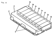
- a dielectric filter formed by coupling a plurality of individual dielectric coaxial resonators has a structure, in which a plurality of dielectric coaxial resonators 1a to 1h is mounted on the upper surface of a substrate 2, to which a metal cover is attached to cover the substrate 2 and the plurality of dielectric coaxial resonators 1a to 1h so as to electrically connect the metal cover 3 to grounding electrodes 4 on the substrate 2.
- This figure shows a view obtained by seeing through the metal cover 3.
- Japanese Unexamined Patent Application Publication No. 7-235805 discloses a resonator device in which the upper surfaces of dielectric coaxial resonators are exposed while the other parts thereof are covered by a metal cover.
- the structure in which only the coupling parts of the dielectric coaxial resonators are covered by the metal cover causes a problem.
- a dielectric resonator device including a plurality of dielectric coaxial resonators having outer conductors and inner conductors, a substrate having the plurality of dielectric coaxial resonators disposed thereon, and a metal cover connected to grounding electrodes of the substrate.
- one specified dielectric coaxial resonator of the plurality of dielectric coaxial resonators is separated from the adjacent dielectric coaxial resonator by a specified gap, the metal member does not cover the upper surfaces of the plurality of dielectric coaxial resonators, and a part of the metal member allows the outer conductors of the dielectric coaxial resonators to be electrically connected to each other in the specified gap.
- the metal member may cover at least one of an area close to open-circuited faces of the dielectric coaxial resonators and an area where terminals electrically connected to the inner conductors of the dielectric coaxial resonators are led out.
- the part of the metal member may be bonded to the outer conductors of the dielectric coaxial resonators by a conductive bonding agent in the specified gap.
- grounding electrodes may be formed near the part of the metal member that may be flexible.
- the metal member may be formed by a metal plate, and the part of the metal member may be subjected to bending. With this arrangement, rigidity of the part of the metal member is increased, and areas where the part of the metal member is bonded to the outer conductors of the dielectric coaxial resonators are also increased.
- the part of the metal member may be subjected to ribbing.
- This increases the rigidity of the part of the metal member and can also improve bonding reliability.
- a punched hole may be formed in the part of the metal member. With this arrangement, like the case of ribbing, bonding reliability can be improved.
- a dielectric duplexer including the dielectric resonator device described above, and a transmission filter and a reception filter formed by the plurality of dielectric coaxial resonators used in the dielectric resonator device.
- the dielectric coaxial resonators of the transmission filter are separated from the adjacent dielectric coaxial resonators of the reception filter by the specified gap.
- a communication apparatus including one of the dielectric resonator device and the dielectric duplexer described above.
- Fig. 1 is a perspective view of the appearance of a dielectric duplexer.
- Fig. 2 is a perspective view of the appearance of only a metal cover used in the above dielectric duplexer.
- reference numerals 1a, 1b, 1c, 1d, 1e, and 1f denote dielectric coaxial resonators having outer conductors formed on the outer surfaces of rectangular-parallelepiped dielectric members. Through-holes are formed in the central axes of the dielectric members, and inner conductors are formed on the inner surfaces of the through-holes. In a direction shown in Fig.
- the outer conductors are formed to be short-circuited, and on the left front end faces thereof, no outer conductors are formed to be open-circuited.
- Pin terminals electrically connected to the inner conductor are inserted in the through-holes of the dielectric coaxial resonators 1a to 1f.
- the outer conductors of the dielectric coaxial resonators 1a to 1f are bonded to grounding electrodes 4 disposed on the upper surfaces of a substrate 2 by using a conductive boding agent such as solder.
- Reference numeral 3 denotes a metal cover. As also shown in Fig. 2, the metal cover 3 is formed by stamping and bending a metal plate.
- the metal cover 3 has protrusions 5 protruding in the axial directions of the dielectric coaxial resonators and conductive side portions 6 electrically connected to side surfaces of the outermost dielectric coaxial resonators of the aligned dielectric coaxial resonators formed in a state in which the metal cover 3 is bonded to the substrate 2.
- grounding terminals 9 connected to the grounding electrodes 4 of the substrate 2 and projections 10 for determining a position with respect to the substrate 2.
- the grounding terminals 9 of the metal cover 3 are soldered to the grounding electrodes 4 on the substrate 2.
- the protrusions 5 of the metal cover 3 are interposed between the dielectric coaxial resonators 1a and 1b and between the dielectric coaxial resonators 1b and 1c, and the outer conductors of the mutually adjacent dielectric coaxial resonators 1a, 1b, and 1c are bonded to each other by using a conductive bonding agent such as solder. Since the protrusions 5 of the metal cover 3 are subjected to bending, rigidity of the protrusions 5 is increased particularly in a direction parallel to the substrate 2.
- the protrusions 5 can be reliably connected to the outer conductors of the dielectric coaxial resonators.
- the positioning projections 10 disposed on the metal cover 3 are inserted in the holes of the substrate 2 to set the position of the metal cover 3 with respect to the substrate 2. Furthermore, when the dielectric coaxial resonators 1a to 1f are disposed on the substrate with the metal cover 3 by soldering, since the positioning of the dielectric coaxial resonators 1a to 1f is performed by the protrusions 5 of the metal cover 3 and the conductive side portions 6, the positional relationships between the substrate 2, the metal cover 3, and the dielectric coaxial resonators 1a to 1f can be easily maintained fixed. As a result, in mass production of the dielectric resonator devices, stable filter characteristics can be obtained.
- the outer conductors of the dielectric coaxial resonators can be electrically connected to the metal cover without soldering.
- Fig. 3 shows the circuit diagram of the dielectric duplexer.
- Reference numerals Ra to Rf denote resonators corresponding to the dielectric coaxial resonators 1a to 1f shown in Fig. 1.
- the resonators Ra and Rb are disposed between a transmitted-signal input port Tx and an antenna port ANT via capacitors and inductors having specified electrical lengths.
- the resonators Rc to Rf which are connected in sequence via capacitors, are disposed between the antenna port ANT and a received-signal output port Rx.
- the above arrangement forms a transmission filter constituted of the two resonators Ra and Rb, which has band-blocking-type filter characteristics, and a reception filter constituted of the four resonators Rc to Rf, which has band-pass-type filter characteristics.
- the dielectric coaxial resonators 1a and 1b shown in Fig. 1 form the transmission filter handling a relatively large amount of electric power, when ground connection is performed without fail by the protrusions 5 and the conductive side portions 6 of the metal cover 3, deterioration of the attenuation characteristics caused by detouring of the ground-current path can be prevented.
- the protrusions 5 of the metal cover 3 are electrically connected between the dielectric coaxial resonator 1b as the last-stage resonator of the transmission filter and the dielectric coaxial resonator 1c as the first-stage resonator of the reception filter. With this arrangement, entering of a transmitted signal into the reception filter caused by detouring of the ground current can also be prevented without fail.
- Fig. 4 is a perspective view of the appearance of the dielectric filter
- Fig. 5 is a perspective view of the appearance of only a metal cover of the dielectric filter.
- reference numerals 1a, 1b, and 1c denote the same dielectric coaxial resonators as those used in the first embodiment.
- Outer conductors of the dielectric coaxial resonators 1a to 1c are bonded to grounding electrodes on the upper surface of a substrate 2 by using a conductive bonding agent.
- Reference numeral 3 denotes a metal cover. As also shown in Fig. 5, the metal cover 3 is formed by stamping and bending a metal plate.
- the metal cover 3 In a state in which the metal cover is bonded to the substrate 2, the metal cover 3 has protrusions 5 protruding in the axial direction of the dielectric coaxial resonators and the conductive side portions 6 electrically connected to the side surfaces of the outermost dielectric coaxial resonators of the aligned dielectric coaxial resonators.
- grounding terminals 9 connected to the grounding electrodes of the substrate 2 and projections 10 for setting the position of the metal cover 3 with respect to the substrate 2.
- the grounding terminals 9 of the metal cover 3 are soldered to the grounding electrodes 4 on the substrate 2.
- the protrusions 5 of the metal cover 3 are interposed between the dielectric coaxial resonators 1a and 1b and between the dielectric coaxial resonators 1b and 1c, and the outer conductors of the mutually adjacent dielectric coaxial resonators 1a, 1b, and 1c are bonded to each other by a conductive bonding agent such as solder.
- a conductive bonding agent such as solder.
- Fig. 6 shows a circuit diagram of the above dielectric filter.
- Reference numerals Ra to Rc denote resonators corresponding to the dielectric coaxial resonators 1a and 1c shown in Fig. 4.
- the resonators Ra to Rc which are connected in sequence via capacitors, are disposed between an input port IN and an output port OUT.
- the above arrangement forms a dielectric filter constituted of the resonators Ra to Rc of three stages, which has band-pass-type filter characteristics.
- Fig. 7 is a perspective view of the appearance of the dielectric filter
- Fig. 8 is a perspective view of the appearance of only a metal cover of the dielectric filter.
- reference numerals 1a, 1b, and 1c denote the same dielectric coaxial resonators as those used in the first embodiment.
- Outer conductors of the dielectric coaxial resonators 1a to 1c are bonded to grounding electrodes 4 on the upper surface of a substrate 2 by using a conductive bonding agent such as solder.
- Reference numeral 3 denotes a metal cover.
- the metal cover is formed by stamping and bending a metal plate.
- the metal cover 3 In a state in which the metal cover 3 is bonded to the substrate 2, the metal cover 3 has protrusions 5 protruding in the axial direction of the dielectric coaxial resonators and grounding terminals 9 connected to the grounding electrodes 4 of the substrate 2.
- the grounding terminals 9 of the metal cover 3 are soldered to the grounding electrodes 4 on the substrate 2.
- the protrusions 5 of the metal cover 3 are interposed between the dielectric coaxial resonators 1a and 1b, and the outer conductors of the mutually adjacent dielectric coaxial resonators 1a and 1b are bonded to each other by a conductive bonding agent such as solder. With this arrangement, the paths of ground currents flowing from the outer conductors of the dielectric coaxial resonators to the grounding electrodes 4 on the substrate can be shortened.
- the dielectric coaxial resonator 1a serves as a trap resonator for a transmission filter.
- the dielectric coaxial resonators 1b and 1c serve as the two-stage resonator of a reception filter.
- the protrusion 5 of the metal cover 3 is subjected to bending and has two surfaces parallel to the mutually opposing outer surfaces of the dielectric coaxial resonators 1a and 1b.
- rigidity of the protrusion 5 is increased and the deformation thereof is thereby prevented.
- positional accuracy between the metal cover 3 and the plurality of dielectric coaxial resonators can be improved.
- the areas in which the protrusion 5 is bonded to the outer conductors of the dielectric coaxial resonators can be increased, so that ground connection can be more reliably performed.
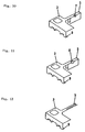
- a protrusion 5 of a metal cover 3 is subjected to bending. Unlike the example shown in Fig. 8, only one side of the protrusion 5 is subjected to bending.
- the protrusion 5 has a surface along the outer surface of one of the adjacent two dielectric coaxial resonators. With this configuration, rigidity of the protrusion 5 can be improved, and also bending can be facilitated.
- a protrusion 5 of a metal cover 3 is subjected to bending, and a rib 7 is formed in the protrusion 5 by ribbing.
- rigidity of the protrusion 5 can be more increased.
- the rib 7 serves as a groove for guiding the flow of solder between the metal cover 3 and side surfaces of the dielectric coaxial resonators, bonding when soldered can also be enhanced.
- a punched hole 8 is formed in a protrusion 5 of a metal cover 3, and the protrusion 5 is subjected to bending.
- the punched hole 8 serves as a groove for guiding the flow of solder between the metal cover 3 and the side surfaces of the dielectric coaxial resonators.
- soldering strength can be increased as in the case of ribbing.
- a protrusion 5 of a metal cover 3 is subjected to bending, the surface along the outer surfaces of the dielectric coaxial resonators is not formed. Instead, the protrusion 5 is bent into a V-letter form or a reversed V-letter form. In this arrangement, an area for the used metal plate can be reduced, and deformation due to bending is also small. Thus, forming processing of the protrusion 5 can be facilitated.
- the shortened path of a ground current is generated from the side surfaces of specified dielectric coaxial resonators to the grounding electrodes on the substrate via the metal cover.
- deterioration of filter characteristics associated with the miniaturization of the metal cover can be prevented.
- rigidity of the protrusion of the metal cover can be increased, and the area where the protrusion of the metal cover is bonded to the outer conductors of the dielectric coaxial resonators can be expanded. As a result, a more reliable ground connection can be implemented.
- rigidity of the protrusion of the metal cover and conductivity between the protrusion of the metal cover and the outer conductors of the adjacent two dielectric coaxial resonators can be provided. Moreover, forming of the protrusion can be facilitated.
- the strength of the protrusion can be maintained even when the width of the protrusion is made narrower. Moreover, since the rib serves as a groove for guiding the in-flow of the conductive bonding agent such as solder, bonding strength and conductivity can be enhanced.
- the punched hole serves as a groove for guiding the in-flow of the conductive bonding agent such as solder, bonding strength and conductivity can be enhanced.
- the ground connection of the last-stage resonator of the transmission filter and the first-stage resonator of the reception filter can be performed without fail. Therefore, entering of a transmitted signal to the reception filter and entering of a received signal to the transmission filter can be reliably prevented. As a result, specified characteristics as a duplexer can be obtained.
- the communication apparatus obtained in the invention is overall compact and has communication performance capabilities using specified filter characteristics.
Landscapes
- Physics & Mathematics (AREA)
- Electromagnetism (AREA)
- Control Of Motors That Do Not Use Commutators (AREA)
- Shielding Devices Or Components To Electric Or Magnetic Fields (AREA)
Abstract
Description
Claims (11)
- A dielectric resonator device comprising:a plurality of dielectric coaxial resonators (1a-1f; 1a-1c) having outer conductors and inner conductors;a substrate (2) having the plurality of dielectric coaxial resonators (1a-1f; 1a-1c) disposed thereon; anda metal member (3) connected to grounding electrodes (4) of the substrate (2);
wherein one specified dielectric coaxial resonator (1a, 1b; 1a) of the plurality of dielectric coaxial resonators (1a-1f; 1a-1c) is separated from the adjacent dielectric coaxial resonator by a specified gap;the metal member (3) does not cover the upper surfaces of the plurality of dielectric coaxial resonators (1a-1f; 1a-1c); anda part of the metal member (3) allows the outer conductors of the dielectric coaxial resonators (1a-1f; 1a-1c) to be electrically connected to each other in the specified gap. - A dielectric resonator device according to Claim 1, wherein the metal member (3) covers at least one of an area close to open-circuited faces of the dielectric coaxial resonators (1a-1f; 1a-1c) and an area where terminals electrically connected to the inner conductors of the dielectric coaxial resonators (1a-1f; 1a-1c) are led out.
- A dielectric resonator device according to Claim 1 or 2, wherein the part of the metal member (3) is bonded to the outer conductors of the dielectric coaxial resonators (1a-1f; 1a-1c) by a conductive bonding agent in the specified gap.
- A dielectric resonator device according to any of Claims 1-3, wherein the grounding electrodes (4) are formed near the part of the metal member (3).
- A dielectric resonator device according to any of Claims 1-4, wherein the part of the metal member (3) is flexible.
- A dielectric resonator device according to any of Claims 1-5, wherein the metal member (3) is formed by a metal plate, and the part of the metal member (3) is subjected to bending.
- A dielectric resonator device according to any of Claims 1-6, wherein the metal member (3) is formed by a metal plate, and the part of the metal member (3) is subjected to ribbing.
- A dielectric resonant device according to any of Claims 1-7, wherein the metal member (3) is formed by a metal plate, and a punched hole (8) is formed in the part of the metal member.
- A dielectric duplexer comprising:the dielectric resonator device according to one of Claims 1 to 8; anda transmission filter and a reception filter formed by the plurality of dielectric coaxial resonators (1a-1f; 1a-1c) used in the dielectric resonator device;
wherein the dielectric coaxial resonators (1a, 1b; 1a) of the transmission filter are separated from the adjacent dielectric coaxial resonators (1c-1f; 1b, 1c) of the reception filter by the specified gap. - A communication apparatus comprising the dielectric resonator device according to one of Claims 1 to 8.
- A communication apparatus comprising the dielectric duplexer according to Claim 9.
Applications Claiming Priority (2)
| Application Number | Priority Date | Filing Date | Title |
|---|---|---|---|
| JP26001399A JP3444246B2 (en) | 1999-09-14 | 1999-09-14 | Dielectric resonator device, dielectric duplexer, and communication device |
| JP26001399 | 1999-09-14 |
Publications (3)
| Publication Number | Publication Date |
|---|---|
| EP1085593A2 true EP1085593A2 (en) | 2001-03-21 |
| EP1085593A3 EP1085593A3 (en) | 2002-09-18 |
| EP1085593B1 EP1085593B1 (en) | 2008-05-21 |
Family
ID=17342106
Family Applications (1)
| Application Number | Title | Priority Date | Filing Date |
|---|---|---|---|
| EP00118856A Expired - Lifetime EP1085593B1 (en) | 1999-09-14 | 2000-08-31 | Dielectric resonator device, dielectric duplexer, and communication apparatus incorporating same |
Country Status (5)
| Country | Link |
|---|---|
| US (1) | US6573809B1 (en) |
| EP (1) | EP1085593B1 (en) |
| JP (1) | JP3444246B2 (en) |
| KR (1) | KR100343895B1 (en) |
| DE (1) | DE60038929D1 (en) |
Cited By (2)
| Publication number | Priority date | Publication date | Assignee | Title |
|---|---|---|---|---|
| WO2005069426A1 (en) * | 2004-01-13 | 2005-07-28 | Epcos Ag | Low-rise duplexer comprising shielding |
| WO2021190241A1 (en) * | 2020-03-27 | 2021-09-30 | 深圳顺络电子股份有限公司 | Ceramic filter having cte compensation function |
Families Citing this family (1)
| Publication number | Priority date | Publication date | Assignee | Title |
|---|---|---|---|---|
| CN211829141U (en) * | 2020-06-04 | 2020-10-30 | 深圳顺络电子股份有限公司 | Ceramic dielectric filter |
Family Cites Families (12)
| Publication number | Priority date | Publication date | Assignee | Title |
|---|---|---|---|---|
| JPS59171401U (en) * | 1983-05-02 | 1984-11-16 | 株式会社村田製作所 | Fixing and connection structure of dielectric coaxial resonator |
| JPS62141802A (en) * | 1985-12-16 | 1987-06-25 | Murata Mfg Co Ltd | Fixing structure for dielectric coaxial resonator |
| JPH0621701A (en) * | 1992-06-30 | 1994-01-28 | Taiyo Yuden Co Ltd | Filter inclusing dielectric resonator |
| US5278527A (en) * | 1992-07-17 | 1994-01-11 | Motorola, Inc. | Dielectric filter and shield therefor |
| JPH07142906A (en) * | 1993-11-15 | 1995-06-02 | Fuji Elelctrochem Co Ltd | Dielectric filter lid mounting structure |
| JPH07170104A (en) * | 1993-12-13 | 1995-07-04 | Sony Corp | Surface mount components using dielectric resonator |
| JPH07235805A (en) * | 1994-02-22 | 1995-09-05 | Murata Mfg Co Ltd | Dielectric filter |
| JPH07240604A (en) * | 1994-02-25 | 1995-09-12 | Murata Mfg Co Ltd | Dielectric resonator device |
| JP2907010B2 (en) * | 1994-08-03 | 1999-06-21 | 松下電器産業株式会社 | Dielectric filter |
| JPH1079605A (en) * | 1996-09-03 | 1998-03-24 | Tokin Corp | Antenna duplexer |
| JPH10261880A (en) * | 1997-03-19 | 1998-09-29 | Tokin Corp | Metal case for dielectric filter and dielectric filter |
| JPH10308607A (en) * | 1997-05-07 | 1998-11-17 | Ngk Spark Plug Co Ltd | Dielectric duplexer device |
-
1999
- 1999-09-14 JP JP26001399A patent/JP3444246B2/en not_active Expired - Fee Related
-
2000
- 2000-08-31 EP EP00118856A patent/EP1085593B1/en not_active Expired - Lifetime
- 2000-08-31 DE DE60038929T patent/DE60038929D1/en not_active Expired - Lifetime
- 2000-09-08 KR KR1020000053389A patent/KR100343895B1/en not_active Expired - Fee Related
- 2000-09-14 US US09/661,213 patent/US6573809B1/en not_active Expired - Lifetime
Cited By (2)
| Publication number | Priority date | Publication date | Assignee | Title |
|---|---|---|---|---|
| WO2005069426A1 (en) * | 2004-01-13 | 2005-07-28 | Epcos Ag | Low-rise duplexer comprising shielding |
| WO2021190241A1 (en) * | 2020-03-27 | 2021-09-30 | 深圳顺络电子股份有限公司 | Ceramic filter having cte compensation function |
Also Published As
| Publication number | Publication date |
|---|---|
| EP1085593B1 (en) | 2008-05-21 |
| US6573809B1 (en) | 2003-06-03 |
| KR100343895B1 (en) | 2002-07-20 |
| KR20010050395A (en) | 2001-06-15 |
| JP3444246B2 (en) | 2003-09-08 |
| EP1085593A3 (en) | 2002-09-18 |
| DE60038929D1 (en) | 2008-07-03 |
| JP2001085906A (en) | 2001-03-30 |
Similar Documents
| Publication | Publication Date | Title |
|---|---|---|
| KR101089195B1 (en) | Input / output coupling structure of dielectric waveguide | |
| JP2004023567A (en) | Mounting structure for dielectric filter, dielectric filter device, and mounting structure for dielectric duplexer and communication equipment system | |
| KR100312588B1 (en) | Dielectric Filter, Dielectric Duplexer, and Communication Apparatus Using The Same | |
| EP0959518B1 (en) | Dielectric filter, dielectric duplexer, and transceiver | |
| US6236291B1 (en) | Dielectric filter, duplexer, and communication device | |
| EP0738023A2 (en) | Antenna device | |
| KR100397738B1 (en) | Nonreciprocal circuit device and mounting structure of the same | |
| EP1085593B1 (en) | Dielectric resonator device, dielectric duplexer, and communication apparatus incorporating same | |
| EP0982792B1 (en) | Antenna duplexer and communication apparatus | |
| KR100470311B1 (en) | Nonreciprocal circuit device and communication apparatus | |
| CN1329763A (en) | Microstrip filter device | |
| KR100326949B1 (en) | Dielectric filter, transmission/reception sharing device and communication device | |
| JP3539351B2 (en) | Method for manufacturing non-reciprocal circuit device | |
| JP2001094311A (en) | Non-reversible circuit element and communication machine equipment | |
| EP1107348A2 (en) | Nonreciprocal circuit device, nonreciprocal circuit and communication device | |
| JP3425702B2 (en) | Antenna duplexer | |
| US6137382A (en) | Dielectric duplexer and a communication device including such dielectric duplexer | |
| JP4438228B2 (en) | Isolator and communication device | |
| JP2000068717A (en) | Dielectric oscillation parts, dielectric filter, antenna multicoupler, composite filter and communication equipment | |
| JP2007295361A (en) | Duplexer | |
| KR20020062584A (en) | Dielectric duplexer and communication apparatus | |
| JPH10242709A (en) | Dielectric duplexer | |
| JP2000091811A (en) | Filter device | |
| JPH0681102U (en) | Dielectric filter | |
| JPH1028004A (en) | Electronic parts for high frequency |
Legal Events
| Date | Code | Title | Description |
|---|---|---|---|
| PUAI | Public reference made under article 153(3) epc to a published international application that has entered the european phase |
Free format text: ORIGINAL CODE: 0009012 |
|
| 17P | Request for examination filed |
Effective date: 20000831 |
|
| AK | Designated contracting states |
Kind code of ref document: A2 Designated state(s): AT BE CH CY DE DK ES FI FR GB GR IE IT LI LU MC NL PT SE |
|
| AX | Request for extension of the european patent |
Free format text: AL;LT;LV;MK;RO;SI |
|
| PUAL | Search report despatched |
Free format text: ORIGINAL CODE: 0009013 |
|
| AK | Designated contracting states |
Kind code of ref document: A3 Designated state(s): AT BE CH CY DE DK ES FI FR GB GR IE IT LI LU MC NL PT SE |
|
| AX | Request for extension of the european patent |
Free format text: AL;LT;LV;MK;RO;SI |
|
| AKX | Designation fees paid |
Designated state(s): DE FR GB |
|
| 17Q | First examination report despatched |
Effective date: 20061215 |
|
| RAP1 | Party data changed (applicant data changed or rights of an application transferred) |
Owner name: MURATA MANUFACTURING CO., LTD. |
|
| GRAP | Despatch of communication of intention to grant a patent |
Free format text: ORIGINAL CODE: EPIDOSNIGR1 |
|
| GRAS | Grant fee paid |
Free format text: ORIGINAL CODE: EPIDOSNIGR3 |
|
| GRAA | (expected) grant |
Free format text: ORIGINAL CODE: 0009210 |
|
| AK | Designated contracting states |
Kind code of ref document: B1 Designated state(s): DE FR GB |
|
| REG | Reference to a national code |
Ref country code: GB Ref legal event code: FG4D |
|
| REF | Corresponds to: |
Ref document number: 60038929 Country of ref document: DE Date of ref document: 20080703 Kind code of ref document: P |
|
| PLBE | No opposition filed within time limit |
Free format text: ORIGINAL CODE: 0009261 |
|
| STAA | Information on the status of an ep patent application or granted ep patent |
Free format text: STATUS: NO OPPOSITION FILED WITHIN TIME LIMIT |
|
| 26N | No opposition filed |
Effective date: 20090224 |
|
| GBPC | Gb: european patent ceased through non-payment of renewal fee |
Effective date: 20080831 |
|
| PG25 | Lapsed in a contracting state [announced via postgrant information from national office to epo] |
Ref country code: GB Free format text: LAPSE BECAUSE OF NON-PAYMENT OF DUE FEES Effective date: 20080831 |
|
| REG | Reference to a national code |
Ref country code: FR Ref legal event code: ST Effective date: 20110708 |
|
| PG25 | Lapsed in a contracting state [announced via postgrant information from national office to epo] |
Ref country code: FR Free format text: LAPSE BECAUSE OF NON-PAYMENT OF DUE FEES Effective date: 20080901 |
|
| PGFP | Annual fee paid to national office [announced via postgrant information from national office to epo] |
Ref country code: DE Payment date: 20140827 Year of fee payment: 15 |
|
| REG | Reference to a national code |
Ref country code: DE Ref legal event code: R119 Ref document number: 60038929 Country of ref document: DE |
|
| PG25 | Lapsed in a contracting state [announced via postgrant information from national office to epo] |
Ref country code: DE Free format text: LAPSE BECAUSE OF NON-PAYMENT OF DUE FEES Effective date: 20160301 |