EP1084009B1 - Cmp pad conditioner arrangement and method therefor - Google Patents
Cmp pad conditioner arrangement and method therefor Download PDFInfo
- Publication number
- EP1084009B1 EP1084009B1 EP00919794A EP00919794A EP1084009B1 EP 1084009 B1 EP1084009 B1 EP 1084009B1 EP 00919794 A EP00919794 A EP 00919794A EP 00919794 A EP00919794 A EP 00919794A EP 1084009 B1 EP1084009 B1 EP 1084009B1
- Authority
- EP
- European Patent Office
- Prior art keywords
- pad
- arrangement
- cmp
- cmp pad
- pad conditioner
- Prior art date
- Legal status (The legal status is an assumption and is not a legal conclusion. Google has not performed a legal analysis and makes no representation as to the accuracy of the status listed.)
- Expired - Lifetime
Links
Images


Classifications
-
- H—ELECTRICITY
- H10—SEMICONDUCTOR DEVICES; ELECTRIC SOLID-STATE DEVICES NOT OTHERWISE PROVIDED FOR
- H10P—GENERIC PROCESSES OR APPARATUS FOR THE MANUFACTURE OR TREATMENT OF DEVICES COVERED BY CLASS H10
- H10P52/00—Grinding, lapping or polishing of wafers, substrates or parts of devices
-
- B—PERFORMING OPERATIONS; TRANSPORTING
- B24—GRINDING; POLISHING
- B24B—MACHINES, DEVICES, OR PROCESSES FOR GRINDING OR POLISHING; DRESSING OR CONDITIONING OF ABRADING SURFACES; FEEDING OF GRINDING, POLISHING, OR LAPPING AGENTS
- B24B53/00—Devices or means for dressing or conditioning abrasive surfaces
- B24B53/017—Devices or means for dressing, cleaning or otherwise conditioning lapping tools
-
- B—PERFORMING OPERATIONS; TRANSPORTING
- B24—GRINDING; POLISHING
- B24B—MACHINES, DEVICES, OR PROCESSES FOR GRINDING OR POLISHING; DRESSING OR CONDITIONING OF ABRADING SURFACES; FEEDING OF GRINDING, POLISHING, OR LAPPING AGENTS
- B24B53/00—Devices or means for dressing or conditioning abrasive surfaces
- B24B53/013—Application of loose grinding agent as auxiliary tool during truing operation
-
- B—PERFORMING OPERATIONS; TRANSPORTING
- B24—GRINDING; POLISHING
- B24D—TOOLS FOR GRINDING, BUFFING OR SHARPENING
- B24D13/00—Wheels having flexibly-acting working parts, e.g. buffing wheels; Mountings therefor
- B24D13/14—Wheels having flexibly-acting working parts, e.g. buffing wheels; Mountings therefor acting by the front face
- B24D13/145—Wheels having flexibly-acting working parts, e.g. buffing wheels; Mountings therefor acting by the front face having a brush-like working surface
-
- B—PERFORMING OPERATIONS; TRANSPORTING
- B24—GRINDING; POLISHING
- B24D—TOOLS FOR GRINDING, BUFFING OR SHARPENING
- B24D13/00—Wheels having flexibly-acting working parts, e.g. buffing wheels; Mountings therefor
- B24D13/18—Wheels having flexibly-acting working parts, e.g. buffing wheels; Mountings therefor with cooling provisions
Definitions
- the present device relates generally to semiconductor devices and their fabrication and, more particularly, to semiconductor devices and tools for their manufacture involving chemical-mechanical polishing (CMP), as for example known from document JP-A-110 105 24.
- CMP chemical-mechanical polishing
- a byproduct of the increased complexity of semiconductor devices includes uneven device surfaces, which become more prominent as additional levels are added to multilevel-interconnection schemes and circuit features are scaled to submicron dimensions.
- each level within the device is patterned, resulting in a surface with varied "step-heights" where metal forming the pattern remains on the surface.
- Planarization is a term describing the surface geometry of a semiconductor device. Complete planarization occurs when the surface of the dielectric is flat, as in a plane. No planarization occurs when the surface of the dielectric directly models the "step-height" surface of the metal pattern in the layer underneath.
- the degree of planarization refers to the degree to which the varied surface geometry can be “planarized,” or smoothed out into a planar surface. Varied surface geometry is often undesirable. Therefor, as additional layers are formed within devices, the required degree of planarization increases.
- CMP chemical-mechanical polishing
- a CMP process involves securing a semiconductor wafer to a wafer holder with the wafer located face-down on a polish pad. Both the polish pad and the wafer rotate.
- a slurry typically a colloidal silica that is a suspension of SiO 2 particles, is applied to the process. The particle size typically varies from 100 angstroms to 3 microns.
- the slurry is generally applied using a wand feeding to the wafer holder and pad.
- the rate of removal of material from the wafer is a combination of chemical and mechanical rates. The mechanical removal rate is roughly proportional to the pressure and the relative velocity of the wafer.
- the chemical removal rate is a function of the size of the slurry particles and the solution pH, wherein the maximum removal rate is generally obtained using a slurry having a pH of about 11.5.
- a conditioner is also typically used for conditioning the polish pad.
- the conditioner aids in the CMP polishing process and contributes to the longevity of the pad.
- Another need in the CMP process is for adequately and efficiently cleaning the pad and the wafer itself. In clean room environments, it is important to maintain a CMP process that produces as few contaminants as possible. Since the slurry particle size ranges in the sub-3 micron range, clean-up is difficult and thus of high importance. In addition, it is helpful to prevent the byproduct resulting from the polishing of each wafer from accumulating on the pad and reaching additional wafers.
- the traditional method for conditioning the pad and dispensing slurry is to use two separate mechanical components: a slurry dispense wand and a pad conditioner assembly.
- a slurry dispense wand and a pad conditioner assembly.
- the slurry cannot be spread uniformly across the pad and may accumulate in the pad conditioning head. The non-uniform distribution of slurry distribution hinders the polishing process.
- the reaction byproduct cannot be thoroughly removed from the pad. When more than one wafer is processed at once, inadequate cleaning of the pad results in the reaction byproduct and other materials from one wafer coming into contact with other wafers.
- These disadvantages may result in, for example, long arc style scratches, shallow micro-scratches, inter-die thickness variation, and residual slurry particles. These disadvantages ultimately result in a significant yield lost and in reliability problems due in part to possible metal stringers in the shallow scratch area and surrounding residual slurry particles.
- the present invention is directed to a method and apparatus for improving the CMP process, the improvements including but not limited to enhanced pad cleaning and conditioning, better slurry dispense, improved wafer quality, and faster production.
- the present invention is exemplified in a number of implementations and applications, some of which are summarized below.
- the present invention comprises a CMP pad conditioner arrangement comprising the features of claim 1.
- the present invention is directed to a method of conditioning a CMP pad comprising the features of claim 7.
- the present invention is directed to a method of manufacturing a semiconductor device comprising the features of claim 8.
- the present invention is directed to an arrangement for use in a CMP process.
- the arrangement includes capabilities for receiving, dispersing, and dispensing treatment elements, as well as for conditioning the CMP pad.
- the arrangement may also include the capability of rotation.
- the conditioning of the pad may include, for example, removing deposits, roughing the pad, or other preparations for use in the CMP process.
- the arrangement includes an inlet port for receiving treatment elements.
- a distribution surface is coupled to the inlet port and is configured and arranged to disperse the treatment elements.
- a multitude of outlet ports are coupled to the distribution surface and are configured and arranged to dispense the treatment elements onto the CMP pad.
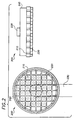
- FIG. 1 shows top and side views of a CMP pad conditioner arrangement 100 for use in a CMP process, according to another embodiment of the present invention.
- Supply 130 is configured and arranged to supply treatment elements to the pad conditioner head 140.
- Pad conditioner head 140 includes holes 110 for dispensing treatment elements to the surface to be conditioned.
- Brushes 120 are coupled to the pad conditioner head 140.
- the brushes may, for instance, comprise chemically resistant material, such as plastic or Teflon. The use of chemically resistant brushes is particularly advantageous in applications where the treatment elements include chemicals that are reactive with non-chemically resistant brush material.
- a method for conditioning a CMP pad is provided.
- supply 130 is coupled to pad conditioner head 140.
- Treatment elements are delivered to the pad conditioner head 140 by way of supply 130.
- the treatment elements may include, for example, chemicals ranging in pH from highly basic to highly acidic, or solvents such as de-ionized (DI) water.
- DI de-ionized
- the treatment elements are dispersed in the head 140, and dispensed through holes 110.
- Brushes 120 are coupled to pad conditioner head 140, and are caused to contact a CMP pad.
- FIG. 2 shows top and side views of a CMP pad conditioner arrangement 200 for use in a CMP process, according to another embodiment of the present invention.
- Supply 230 is configured and arranged to supply treatment elements to the pad conditioner head 240.
- Pad conditioner head 240 includes holes 210, for dispensing treatment elements to the surface to be conditioned.
- Grid arrangement 220 is coupled to the pad conditioner head 240.
- grid arrangement 220 may include material such as diamond or CVD diamond coated with Ni.
- a method for conditioning a CMP pad is provided.
- supply 230 is coupled to pad conditioner head 240.
- Treatment elements are delivered to the pad conditioner head 240 by way of supply 230.
- the treatment elements are dispersed in the head 240, and dispensed through holes 210.
- Grid arrangement 220 is coupled to pad conditioner head 240, and is caused to contact a CMP pad.
- the treatment elements are dispersed onto the CMP pad, and the CMP pad is conditioned.
- Conditioning the CMP pad may, for instance, also include rotating the pad conditioner head 240, in a manner such as rotating about its center using a motor/axle arrangement (not shown) coupled to the housing for the supply 230 (or 130).
- FIG. 3 shows top and side views of a CMP pad conditioner arrangement 300 for cleaning a pad in a CMP process, according to another embodiment of the present invention.
- Treatment element supplies 350 and 360 are configured and arranged to supply elements to supply 330.
- Supply 330 is configured and arranged to supply treatment elements to the pad conditioner head 340.
- Pad conditioner head 340 includes holes 310, for dispensing treatment elements to the surface to be conditioned.
- Brushes 320 are coupled to the pad conditioner head 340.
- a method for conditioning a CMP pad is provided.
- treatment element supplies 350 and 360 are coupled to supply 330.
- Supply 330 is coupled to pad conditioner head 340.
- Treatment elements are delivered to pad conditioner head 340 by way of supply 330.
- the treatment elements are dispersed in the head 340, and dispensed through holes 310.
- Brush arrangement 320 is coupled to pad conditioner head 340, and is caused to contact a CMP pad.
- the treatment elements are dispersed onto the CMP pad, and the CMP pad is conditioned.
- Conditioning the CMP pad may, for instance, also include rotating the pad conditioner head 340, in a manner such as rotating about its center.
- Treatment element supplies 350 and 360 may be used to supply several different elements. For instance, one supply may be used to supply chemicals, and the other used to supply DI water.
- pad conditioner arrangement 300 is used in connection with a metal polish process, in which the chemical supply includes a low pH chemical.
- pad conditioner arrangement 300 is used in an oxide polish process, in which the chemical supply includes a high pH chemical, such as, for example, a chemical having a pH of about 11.5.
Landscapes
- Engineering & Computer Science (AREA)
- Mechanical Engineering (AREA)
- Mechanical Treatment Of Semiconductor (AREA)
- Grinding-Machine Dressing And Accessory Apparatuses (AREA)
- Finish Polishing, Edge Sharpening, And Grinding By Specific Grinding Devices (AREA)
Description
Claims (8)
- CMP pad conditioner arrangement (100,200,300), comprisingcharacterized in that the arrangement further comprises:at least one inlet port (130,230,330) for receiving treatment elements;a distribution surface (140,240,340) coupled to the inlet port (130,230,330) and configured and arranged to disperse the treatment elements; anda multitude of outlet ports (110,210,310) coupled to the distribution surface (140,240,340) and configured and arranged to dispense the treatment elements onto a CMP pad,a brush arrangement (120, 320) or a grid arrangement (220), which is arranged to contact the CMP pad, anda rotation device configured to rotate the distribution surface (140,240,340).
- CMP pad conditioner arrangement (100,200,300) according to Claim 1, wherein the distribution surface is present in a pad conditioner head (140,240,340) to which the brush or the grid arrangement (120, 220,320) is coupled.
- CMP pad conditioner arrangement according to Claim 1 or 2, characterized in thatthe pad conditioner arrangement (100,200,300) has an outlet side, at which side the outlet ports (110, 210, 310) are present, andthe brush or grid arrangement (120,220,320) is present at the outlet side, such that the outlet ports (110, 210,3 10) are distributed along that side in between of the brushes or grid parts (120,220,320).
- CMP pad conditioner arrangement (200) according to Claim 3, wherein the brush or grid arrangement is a grid arrangement (220) comprises holes to allow the treatment elements to be dispensed from the outlet ports (210) onto the CMP pad.
- CMP pad conditioner arrangement (100,300) according to Claim 3, wherein the brush or grid arrangement is a brush arrangement (120,320).
- CMP polishing machine comprising the CMP pad conditioner arrangement (100,200,300) according to any of the Claims 1-5.
- A method of conditioning a CMP pad, wherein use is made of the CMP pad conditioner arrangement (100,200,300) according to any of the Claims 1-5 for providing the treatment elements to the CMP pad.
- A method of manufacturing a semiconductor device, in which manufacture a semiconductor wafer is planarized with chemical-mechanical polishing (CMP), which polishing comprises the steps of:securing the semiconductor wafer to a wafer holder having a polishing pad, with the wafer located face-down on the polish pad;applying a slurry to the polish pad, while both the wafer and the polish pad rotate, therewith polishing the wafer and removing material from the wafer, and in addition thereto,conditioning the polish pad, therewith cleaning the pad and in order to remove from the pad reaction byproduct and other material removed from the wafer,in which CMP process use is made of the CMP pad conditioner arrangement (100,200,300) according to any of the Claims 1-5.
Applications Claiming Priority (3)
| Application Number | Priority Date | Filing Date | Title |
|---|---|---|---|
| US283049 | 1999-04-01 | ||
| US09/283,049 US6302771B1 (en) | 1999-04-01 | 1999-04-01 | CMP pad conditioner arrangement and method therefor |
| PCT/US2000/008302 WO2000059681A1 (en) | 1999-04-01 | 2000-03-29 | Cmp pad conditioner arrangement and method therefor |
Publications (2)
| Publication Number | Publication Date |
|---|---|
| EP1084009A1 EP1084009A1 (en) | 2001-03-21 |
| EP1084009B1 true EP1084009B1 (en) | 2004-03-17 |
Family
ID=23084269
Family Applications (1)
| Application Number | Title | Priority Date | Filing Date |
|---|---|---|---|
| EP00919794A Expired - Lifetime EP1084009B1 (en) | 1999-04-01 | 2000-03-29 | Cmp pad conditioner arrangement and method therefor |
Country Status (8)
| Country | Link |
|---|---|
| US (1) | US6302771B1 (en) |
| EP (1) | EP1084009B1 (en) |
| JP (1) | JP2002540965A (en) |
| KR (1) | KR100691031B1 (en) |
| CN (1) | CN1125704C (en) |
| AU (1) | AU4041800A (en) |
| DE (1) | DE60008985T2 (en) |
| WO (1) | WO2000059681A1 (en) |
Families Citing this family (23)
| Publication number | Priority date | Publication date | Assignee | Title |
|---|---|---|---|---|
| JP2001347450A (en) * | 2000-06-08 | 2001-12-18 | Promos Technologies Inc | Chemical mechanical polishing equipment |
| JP3797861B2 (en) * | 2000-09-27 | 2006-07-19 | 株式会社荏原製作所 | Polishing device |
| US6508697B1 (en) * | 2001-07-16 | 2003-01-21 | Robert Lyle Benner | Polishing pad conditioning system |
| TW544374B (en) * | 2002-08-23 | 2003-08-01 | Macronix Int Co Ltd | Conditioner of chemical-mechanical polishing station |
| DE10322496B4 (en) * | 2003-05-18 | 2006-08-24 | Susanne Schiegerl | Device for automatic cleaning and conditioning of polishing cloths used in polishing processes |
| US7052371B2 (en) * | 2003-05-29 | 2006-05-30 | Tbw Industries Inc. | Vacuum-assisted pad conditioning system and method utilizing an apertured conditioning disk |
| CN101817162A (en) * | 2004-01-26 | 2010-09-01 | Tbw工业有限公司 | Multi-step, in-situ pad conditioning system for chemical mechanical planarization |
| US7033253B2 (en) | 2004-08-12 | 2006-04-25 | Micron Technology, Inc. | Polishing pad conditioners having abrasives and brush elements, and associated systems and methods |
| CN100439040C (en) * | 2004-09-02 | 2008-12-03 | 上海宏力半导体制造有限公司 | Polishing Finisher |
| CN101218067B (en) * | 2005-07-09 | 2011-05-18 | Tbw工业有限公司 | Enhanced end effector arm arrangement for CMP pad conditioning |
| US20070087672A1 (en) * | 2005-10-19 | 2007-04-19 | Tbw Industries, Inc. | Apertured conditioning brush for chemical mechanical planarization systems |
| CN102310359B (en) * | 2010-07-01 | 2014-08-20 | 本田技研工业株式会社 | Metal ring grinding device and metal ring grinding method |
| KR101674058B1 (en) * | 2010-10-05 | 2016-11-09 | 삼성전자 주식회사 | Chemical mechanical polishing apparatus having pad conditioning disk, and pre-conditioner unit |
| TWI568538B (en) * | 2013-03-15 | 2017-02-01 | 中國砂輪企業股份有限公司 | Chemical mechanical polishing conditioner and manufacturing method thereof |
| CN103192325B (en) * | 2013-04-10 | 2015-07-15 | 大连理工大学 | Inner-cooling bonded abrasive grinding disc |
| US10293462B2 (en) * | 2013-07-23 | 2019-05-21 | Taiwan Semiconductor Manufacturing Company, Ltd. | Pad conditioner and method of reconditioning planarization pad |
| CN103639902B (en) * | 2013-11-17 | 2016-05-11 | 董朝新 | A kind of using method of the arc shower nozzle of splitter plate type for surface grinding machine emery wheel |
| CN104690648A (en) * | 2013-12-05 | 2015-06-10 | 天津中环领先材料技术有限公司 | Special brush for polishing pad with wax polishing function |
| SG10201906815XA (en) * | 2014-08-26 | 2019-08-27 | Ebara Corp | Substrate processing apparatus |
| CN106272075B (en) * | 2015-05-22 | 2019-05-31 | 中芯国际集成电路制造(上海)有限公司 | Grinding pad trimming device and grinding pad dressing method |
| ES2865159T3 (en) * | 2017-06-30 | 2021-10-15 | Essilor Int | Application device and procedure for cleaning grinding surfaces on an ophthalmic lens grinding machine |
| CN107403362A (en) * | 2017-07-25 | 2017-11-28 | 浙江聚励云机械科技有限公司 | Engineering equipment flat car service system and method |
| CN110625517B (en) * | 2019-07-29 | 2021-04-09 | 华灿光电(浙江)有限公司 | Repairing device and method for substrate flatness detector |
Citations (1)
| Publication number | Priority date | Publication date | Assignee | Title |
|---|---|---|---|---|
| JPH1110524A (en) * | 1997-06-19 | 1999-01-19 | Internatl Business Mach Corp <Ibm> | Wafer carrier assembly for chemical mechanical polishing |
Family Cites Families (19)
| Publication number | Priority date | Publication date | Assignee | Title |
|---|---|---|---|---|
| US3041799A (en) * | 1959-12-31 | 1962-07-03 | Besly Welles Corp | Abrasive disc and coolant arrangement |
| US3074088A (en) * | 1960-12-01 | 1963-01-22 | Walter O Williams | Power brushes for washing automobiles and the like |
| FR2580974B1 (en) * | 1985-04-26 | 1989-05-19 | Lam Plan Sa | POLISHING DEVICE AND METHOD |
| BE1001701A3 (en) * | 1988-05-30 | 1990-02-13 | Diamant Boart Sa | Wheel ball and use thereof for grinding and mechanical polishing glass. |
| FR2633860A1 (en) * | 1988-07-08 | 1990-01-12 | Premines Sa | Rotating support plate for an abrasive disc using water |
| US5384986A (en) * | 1992-09-24 | 1995-01-31 | Ebara Corporation | Polishing apparatus |
| US5607718A (en) * | 1993-03-26 | 1997-03-04 | Kabushiki Kaisha Toshiba | Polishing method and polishing apparatus |
| IT231237Y1 (en) * | 1993-04-26 | 1999-08-02 | Camfart Srl | ABRASIVE WHEEL WITH AERATION HOLES |
| JP2622069B2 (en) * | 1993-06-30 | 1997-06-18 | 三菱マテリアル株式会社 | Dressing equipment for polishing cloth |
| JP3036348B2 (en) * | 1994-03-23 | 2000-04-24 | 三菱マテリアル株式会社 | Truing device for wafer polishing pad |
| JP3734289B2 (en) * | 1995-01-24 | 2006-01-11 | 株式会社荏原製作所 | Polishing device |
| US5667433A (en) * | 1995-06-07 | 1997-09-16 | Lsi Logic Corporation | Keyed end effector for CMP pad conditioner |
| US5616069A (en) * | 1995-12-19 | 1997-04-01 | Micron Technology, Inc. | Directional spray pad scrubber |
| US5664990A (en) * | 1996-07-29 | 1997-09-09 | Integrated Process Equipment Corp. | Slurry recycling in CMP apparatus |
| US5868608A (en) * | 1996-08-13 | 1999-02-09 | Lsi Logic Corporation | Subsonic to supersonic and ultrasonic conditioning of a polishing pad in a chemical mechanical polishing apparatus |
| US5885147A (en) * | 1997-05-12 | 1999-03-23 | Integrated Process Equipment Corp. | Apparatus for conditioning polishing pads |
| US6139406A (en) * | 1997-06-24 | 2000-10-31 | Applied Materials, Inc. | Combined slurry dispenser and rinse arm and method of operation |
| US5916010A (en) * | 1997-10-30 | 1999-06-29 | International Business Machines Corporation | CMP pad maintenance apparatus and method |
| JPH11165266A (en) * | 1997-12-05 | 1999-06-22 | Toshiba Corp | Polishing pad |
-
1999
- 1999-04-01 US US09/283,049 patent/US6302771B1/en not_active Expired - Lifetime
-
2000
- 2000-03-29 CN CN00800916A patent/CN1125704C/en not_active Expired - Fee Related
- 2000-03-29 DE DE60008985T patent/DE60008985T2/en not_active Expired - Lifetime
- 2000-03-29 WO PCT/US2000/008302 patent/WO2000059681A1/en not_active Ceased
- 2000-03-29 EP EP00919794A patent/EP1084009B1/en not_active Expired - Lifetime
- 2000-03-29 AU AU40418/00A patent/AU4041800A/en not_active Abandoned
- 2000-03-29 JP JP2000609225A patent/JP2002540965A/en not_active Withdrawn
- 2000-03-29 KR KR1020007013507A patent/KR100691031B1/en not_active Expired - Fee Related
Patent Citations (1)
| Publication number | Priority date | Publication date | Assignee | Title |
|---|---|---|---|---|
| JPH1110524A (en) * | 1997-06-19 | 1999-01-19 | Internatl Business Mach Corp <Ibm> | Wafer carrier assembly for chemical mechanical polishing |
Also Published As
| Publication number | Publication date |
|---|---|
| JP2002540965A (en) | 2002-12-03 |
| EP1084009A1 (en) | 2001-03-21 |
| KR100691031B1 (en) | 2007-03-09 |
| WO2000059681B1 (en) | 2000-11-30 |
| KR20010052463A (en) | 2001-06-25 |
| DE60008985D1 (en) | 2004-04-22 |
| US6302771B1 (en) | 2001-10-16 |
| WO2000059681A1 (en) | 2000-10-12 |
| AU4041800A (en) | 2000-10-23 |
| CN1310657A (en) | 2001-08-29 |
| DE60008985T2 (en) | 2005-01-27 |
| CN1125704C (en) | 2003-10-29 |
Similar Documents
| Publication | Publication Date | Title |
|---|---|---|
| US6302771B1 (en) | CMP pad conditioner arrangement and method therefor | |
| US6331136B1 (en) | CMP pad conditioner arrangement and method therefor | |
| US6368194B1 (en) | Apparatus for controlling PH during planarization and cleaning of microelectronic substrates | |
| KR100264756B1 (en) | Method for dressing pad, polishing apparatus and method for manufacturing semiconductor device | |
| US7997958B2 (en) | Apparatuses and methods for conditioning polishing pads used in polishing micro-device workpieces | |
| US6409580B1 (en) | Rigid polishing pad conditioner for chemical mechanical polishing tool | |
| US6398627B1 (en) | Slurry dispenser having multiple adjustable nozzles | |
| EP0887153B1 (en) | Combined slurry dispenser and rinse arm | |
| US6350183B2 (en) | High pressure cleaning | |
| US20030168169A1 (en) | Chemical-mechanical polishing apparatus, polishing pad and method for manufacturing semiconductor device | |
| US6390902B1 (en) | Multi-conditioner arrangement of a CMP system | |
| US6213852B1 (en) | Polishing apparatus and method of manufacturing a semiconductor device using the same | |
| KR100398919B1 (en) | Wafer polishing method and polishing pad dressing method | |
| WO2000060645A2 (en) | Dual cmp pad conditioner | |
| WO2002016079A1 (en) | Cmp device and production method for semiconductor device | |
| JP4374038B2 (en) | Substrate processing method | |
| EP1349703B1 (en) | Belt polishing device with double retainer ring | |
| US6517416B1 (en) | Chemical mechanical polisher including a pad conditioner and a method of manufacturing an integrated circuit using the chemical mechanical polisher | |
| JP3646430B2 (en) | Chemical mechanical polishing method and chemical mechanical polishing apparatus | |
| US6211087B1 (en) | Chemical wet etch removal of underlayer material after performing chemical mechanical polishing on a primary layer | |
| US20080220698A1 (en) | Systems and methods for efficient slurry application for chemical mechanical polishing | |
| US6080671A (en) | Process of chemical-mechanical polishing and manufacturing an integrated circuit | |
| KR100257427B1 (en) | Polishing method of semiconductor substrate for forming flat surface shape by polishing semiconductor substrate surface | |
| JP2001219363A (en) | Polishing pad, method for manufacturing polishing pad, and method for manufacturing workpiece using polishing pad | |
| KR19980036066A (en) | Semiconductor manufacturing device |
Legal Events
| Date | Code | Title | Description |
|---|---|---|---|
| PUAI | Public reference made under article 153(3) epc to a published international application that has entered the european phase |
Free format text: ORIGINAL CODE: 0009012 |
|
| AK | Designated contracting states |
Kind code of ref document: A1 Designated state(s): AT BE CH CY DE DK ES FI FR GB GR IE IT LI LU MC NL PT SE |
|
| 17P | Request for examination filed |
Effective date: 20010412 |
|
| 17Q | First examination report despatched |
Effective date: 20020911 |
|
| GRAH | Despatch of communication of intention to grant a patent |
Free format text: ORIGINAL CODE: EPIDOS IGRA |
|
| GRAS | Grant fee paid |
Free format text: ORIGINAL CODE: EPIDOSNIGR3 |
|
| GRAA | (expected) grant |
Free format text: ORIGINAL CODE: 0009210 |
|
| AK | Designated contracting states |
Kind code of ref document: B1 Designated state(s): DE FR GB |
|
| REG | Reference to a national code |
Ref country code: GB Ref legal event code: FG4D |
|
| REG | Reference to a national code |
Ref country code: GB Ref legal event code: 746 Effective date: 20040322 |
|
| REG | Reference to a national code |
Ref country code: IE Ref legal event code: FG4D |
|
| REF | Corresponds to: |
Ref document number: 60008985 Country of ref document: DE Date of ref document: 20040422 Kind code of ref document: P |
|
| ET | Fr: translation filed | ||
| PLBE | No opposition filed within time limit |
Free format text: ORIGINAL CODE: 0009261 |
|
| STAA | Information on the status of an ep patent application or granted ep patent |
Free format text: STATUS: NO OPPOSITION FILED WITHIN TIME LIMIT |
|
| REG | Reference to a national code |
Ref country code: IE Ref legal event code: MM4A |
|
| REG | Reference to a national code |
Ref country code: FR Ref legal event code: D6 |
|
| 26N | No opposition filed |
Effective date: 20041220 |
|
| REG | Reference to a national code |
Ref country code: GB Ref legal event code: 732E |
|
| REG | Reference to a national code |
Ref country code: FR Ref legal event code: TP |
|
| PGFP | Annual fee paid to national office [announced via postgrant information from national office to epo] |
Ref country code: FR Payment date: 20120410 Year of fee payment: 13 |
|
| PGFP | Annual fee paid to national office [announced via postgrant information from national office to epo] |
Ref country code: DE Payment date: 20120223 Year of fee payment: 13 |
|
| PGFP | Annual fee paid to national office [announced via postgrant information from national office to epo] |
Ref country code: GB Payment date: 20120224 Year of fee payment: 13 |
|
| GBPC | Gb: european patent ceased through non-payment of renewal fee |
Effective date: 20130329 |
|
| REG | Reference to a national code |
Ref country code: FR Ref legal event code: ST Effective date: 20131129 |
|
| REG | Reference to a national code |
Ref country code: DE Ref legal event code: R119 Ref document number: 60008985 Country of ref document: DE Effective date: 20131001 |
|
| PG25 | Lapsed in a contracting state [announced via postgrant information from national office to epo] |
Ref country code: GB Free format text: LAPSE BECAUSE OF NON-PAYMENT OF DUE FEES Effective date: 20130329 Ref country code: FR Free format text: LAPSE BECAUSE OF NON-PAYMENT OF DUE FEES Effective date: 20130402 Ref country code: DE Free format text: LAPSE BECAUSE OF NON-PAYMENT OF DUE FEES Effective date: 20131001 |