TECHNICAL FIELD
This invention relates to a novel thermoelectric conversion
material in which pure silicon is made to contain various types of added
element, and more particularly relates to a silicon-based thermoelectric
conversion material having a polycrystal structure, characterized in that the
crystal structure comprises crystal grains composed of a silicon-rich phase,
and a added element-rich phase in which at least one type of added element
is deposited at the grain boundary thereof, the result of which is an
extremely large Seebeck coefficient and low thermal conductivity of 50 W/m·
K or less, allowing the thermoelectric conversion rate to be raised
dramatically, and affording a silicon-based thermoelectric conversion
material composed chiefly of silicon, which is an abundant resource, and
which causes extremely little environmental pollution.
BACKGROUND ART
Thermoelectric conversion elements are devices that are expected
to see practical use because of their efficient utilization of the high levels of
thermal energy required in recent industrial fields. An extremely broad
range of applications have been investigated, such as a system for converting
waste heat into electrical energy, small, portable electric generators for
easily obtaining electricity outdoors, flame sensors for gas equipment, and so
forth.
This conversion efficiency from thermal energy to electrical
energy is a function of the Figure of merit ZT, and rises in proportion to ZT.
This Figure of merit ZT is expressed by Formula 1.
ZT = α2σT/κ
Here, α is the Seebeck coefficient of the thermoelectric material, σ
is the electrical conductivity, κ is the thermal conductivity, and T is the
absolute temperature expressed as the average value for the thermoelectric
element on the high temperature side (TH) and the low temperature side
(TL).
Silicides such as FeSi2 and SiGe, which are thermoelectric
conversion materials that have been known up to now, are abundant natural
resources, but the former has a Figure of merit ZT of 0.2 or less, its
conversion efficiency is low, and its usable temperature range is extremely
narrow, while no decrease in thermal conductivity is seen with the latter
unless the germanium content is about 20 to 30 at%, and germanium is a
scarce resource. Also, silicon and germanium have a state in which there is a
broad liquidus and solidus for complete solid solution, and it is difficult to
produce a uniform composition with melting or ZL (zone leveling), to name
just two of the problems which have impeded industrial application. For
these reasons, the above-mentioned materials have not found widespread
use.
The thermoelectric materials with the highest Figure of merit at
the present time are IrSb3 having a skutterudite-type crystal structure, and
BiTe, PbTe, and other such chalcogen compounds, which are known to
provide highly efficient thermoelectric conversion capability, but from the
standpoint of protecting the global environment, the use of these heavy
metal elements is expected to restricted in the future.
Silicon, meanwhile, has a high Seebeck coefficient, but has
extremely high thermal conductivity, and is therefore not considered
suitable as a high efficiency thermoelectric material, and research into the
thermoelectric characteristics thereof has been limited to silicon with a
carrier concentration of 1018 (M/m3) or less.
DISCLOSURE OF THE INVENTION
The inventors discovered that doping pure silicon with various
elements, such as doping silicon with both a trace amount of a Group III
element or Group V element and a small amount of a Group IV element,
makes it possible to lower thermal conductivity, and the Seebeck coefficient
will be equivalent to or better than that of conventional Si-Ge and Fe-Si
compounds, or will be extremely high at a given carrier concentration. They
also discovered that this material exhibits a good Figure of merit as a
thermoelectric conversion material, without losing the fundamental
advantages afforded by silicon.
The inventors also produced p- and n-type semiconductors by
doping pure silicon with various elements, and examined the relationship of
the doping amount to the thermoelectric characteristics, and as a result
found that up to a doping amount (that is, a carrier concentration) of 1018
(M/m3), the Seebeck coefficient decreases in inverse proportion to the carrier
concentration, but has a maximum value from 1018 to 1019 (M/m3).
It is an object of the present invention to further lower thermal
conductivity or further enhance the Seebeck coefficient and thereby improve
performance, without sacrificing the high Seebeck coefficient and electrical
conductivity had by this novel silicon-based thermoelectric conversion
material discovered by the inventors.
The inventors diligently examined the mechanism by which a high
Seebeck coefficient is obtained with a silicon-based thermoelectric
conversion material doped with various added elements, whereupon they
learned that this novel silicon-based material has a polycrystal structure
having crystal grains composed of a silicon-rich phase, and a added element-rich
phase in which at least one type of added element is deposited at the
grain boundary thereof.
The term "added element" as used here includes elements with
which silicon can be made into a p- or n-type semiconductor, or more
specifically, elements that generate carriers and elements that do not
generate carriers. Therefore, "added element" used by itself refers to both
elements that generate carriers and elements that do not generate carriers,
and when a distinction is to be made, we will refer to elements that generate
carriers, or elements that do not generate carriers.
The "silicon-rich phase" is a crystal phase in which silicon
accounts for at least 80 at% of the crystal grains. The "added element-rich
phase" is a crystal phase in which a added element has been deposited at the
grain boundary of crystal grain composed of a silicon-rich phase,
encompassing everything from depositing just enough to adhere to the
crystal grains to depositing enough to surface the crystal grains in a layer,
depending on the doping amount, and this crystal phase has at least one type
of added element deposited at the grain boundary of these crystal grains. A
case in which a trace amount of silicon is deposited at the grain boundary is
also included.
Specifically, the present invention is thermoelectric conversion
material having a crystal structure in which a added element or a
combination of added elements is or are contained in an amount of 0.001 to
30 at% in silicon, and at least one type of added element is deposited at the
grain boundary of crystal grains in which silicon accounts for at least 80 at%
of the polycrystal structure.
The inventors also investigated a crystal structure in which the
inside of the crystal grains is a silicon-rich phase and the grain boundary is a
added element-rich phase, whereupon they discovered that the conduction of
carriers can be increased in a added element-rich phase in which the added
element cohesion occurs at the grain boundary, and a high Seebeck
coefficient is obtained in the silicon-rich phase (the main phase), which
means that a material with a high Figure of merit is obtained.
In view of this, the inventors tried controlling the crystal structure
aside from composition as a method for keeping the Seebeck coefficient high
and lowering the thermal conductivity, whereupon they found that if the
cooling rate is controlled during melting and solidification, the silicon-rich
phase and added element-rich phase will be dispersed in the required
arrangement within the material, and a material having a high Figure of
merit will be obtained.
Specifically, the present invention is a thermoelectric conversion
material in which the material itself is an ingot quenched from a melt, a
sinter, a heat treated laminate, or a material having a porosity of 5 to 40%.
The present invention is also characterized in that the crystal
grain size and can be kept small (1 to 50 µm) and a thermoelectric conversion
material having the above-mentioned special structure can be obtained by
subjecting the above-mentioned melt to ordinary cooling or quenching,
powderizing the resulting material, and molding and sintering this powder.
The inventors also discovered a method for obtaining a silicon-based
powder for sintering, in which a silicon powder or a silicon-based
powder containing a added element is coated with a added element by
discharge plasma treatment or by a vapor phase growth method such as
vapor deposition, sputtering, or CVD, or is coated with a added element by
plasma treatment using a gas containing the added element, or a added
element is embedded by mechanofusion.
The inventors diligently examined a structure and manufacturing
method with which a silicon-based thermoelectric conversion material
having the above structure could be obtained simply, and as a result learned
that if a layer of silicon or including silicon and a layer including a added
element are formed and laminated alternately, for instance, and then heat
treated, the same structure as that shown in Figure 5 will be obtained for
every layer or in the lamination thickness direction.
The inventors also found that by alternately forming and
laminating layers including silicon (silicon and a added element) with layers
including a added element (in which the added element is the main
component, but silicon is also included), the resulting structure will be two-dimensionally
equivalent to a structure obtained by controlling the cooling
rate during melting and solidification, and will be obtained with a simple
method merely involving forming the above-mentioned material having a
high Figure of merit on a substrate.
The inventors also diligently examined silicon-based
thermoelectric conversion materials in which silicon is doped with a Group
II, Group III, Group V, or Group VI element, a transition metal element, or a
rare earth element. As a result, they noticed that the carrier concentration
resulting from doping that is effective for a thermoelectric conversion
material is 1017 to 1021 (M/m3), and that there is a limit to the doping
amount, whereas the thermal conductivity of the silicon-based material
must be further decreased in order to raise the Figure of merit of the
thermoelectric conversion material.
In view of this, they looked into compositions with which the
thermal conductivity of the material could be greatly decreased and the
Figure of merit markedly improved without lowering the Seebeck coefficient
or electrical conductivity of the silicon-based thermoelectric conversion
material. As a result, they learned that thermal conductivity can be greatly
lowered without changing the carrier concentration in the silicon-based
material by adding carbon, germanium, or tin (Group IV elements) as a
added element that does not generate carriers.
They also learned that when the above-mentioned Group IV
element is added, thermal conductivity decreases sharply up to a doping
amount of 5 at%, and more or less reaches saturation at 10 at%, so a doping
amount of 5 to 10 at% is ideal for lowering thermal conductivity, and
furthermore, the structure must be such that the Group IV element is
deposited at the grain boundary of the silicon-rich phase.
In particular, it was discovered that when germanium is used as
the Group IV element, if the doping amount is small enough that there is no
carrier generation, the germanium is replaced with silicon, resulting in a
diamond-like crystal structure, and furthermore the phonon scattering is
greater because the atomic weight of germanium is different from that of
silicon, allowing the thermal conductivity to be greatly lowered.
The inventors produced ingots of p- and n-type semiconductors
adjusted to a carrier concentration at which the Seebeck coefficient is higher
(1019 to 1021 M/m3) by doping various elements in an amount of 0.05 to 20
at% into a silicon-based thermoelectric conversion material containing a
dopant that generates carriers, after which they examined various methods
for lowering the thermal conductivity of these ingots, and as a result they
perfected the present invention upon discovering that thermal conductivity
can be greatly decreased without sacrificing a high Seebeck coefficient and
low electrical conductivity by making the bulk semiconductor porous.
In short, the silicon-based thermoelectric conversion material
pertaining to the present invention is characterized by having a crystal
structure that is polycrystalline and in which at least one type of added
element is deposited on crystal grains in which silicon accounts for at least
80 at% of the structure, and at the grain boundary thereof. One of the
following methods can be employed to obtain a polycrystal structure such as
this.
A compositional investigation was conducted into reducing the
thermal conductivity of the silicon-based thermoelectric conversion material
of the present invention, which revealed that a composition containing at
least one of carbon, germanium, and tin as a added element that does not
generate carriers, and particularly a composition containing germanium, is
preferable, and that structurally, a lower thermal conductivity will be
obtained by making the bulk semiconductor porous.
BRIEF DESCRIPTION OF THE DRAWINGS
Fig. 1 is a photograph taken by EPMA of the crystal structure of
the thermoelectric conversion material of the present invention
(Si0.97Ge0.03), where A shows the segregation of a germanium added
element, and B shows the segregation of a phosphorus dopant;
Fig. 2 is a photograph taken by EPMA of the crystal structure of
the thermoelectric conversion material of the present invention
(Si0.95Ge0.05), where A shows the segregation of a germanium added
element, and B shows the segregation of a phosphorus dopant;
Fig. 3 is a photograph taken by EPMA of the crystal structure of
the thermoelectric conversion material of the present invention (Si0.9Ge0.1),
where A shows the segregation of a germanium added element, and B shows
the segregation of a phosphorus dopant;
Fig. 4 is a photograph taken by EPMA of the crystal structure of a
comparative material (Si0.85Ge0.15), where A shows the segregation of a
germanium added element, and B shows the segregation of a phosphorus
dopant;
Fig. 5 is a schematic diagram illustrating the crystal structure of
the thermoelectric conversion material of the present invention;
Fig. 6 is a schematic diagram illustrating the state of silicon
particles of the thermoelectric conversion material powder of the present
invention, where A shows the added element on the surface, and B shows the
added element embedded;
Fig. 7 is a diagram illustrating a lamination pattern in the
thermoelectric conversion material of the present invention; and
Fig. 8 is a diagram illustrating another lamination pattern in the
thermoelectric conversion material of the present invention.
BEST MODE FOR CARRYING OUT THE INVENTION
The structure in which the above-mentioned added element-rich
phase is formed at the boundary of the silicon-rich phase, which is a
characteristic feature of the thermoelectric conversion material of the
present invention, will now be described. First, Si1-xGex melts (at%) were
produced by arc melting, with various doping amounts of germanium (4N)
into high purity silicon (10N). These ingots were quenched at a cooling rate
of 50 to 200K/sec after melting to produce sample substrates. The crystal
structure was observed by EPMA.
More specifically, Figure 1A is when x = 0.03, Figure 2A when x
= 0.05, and Figure 3A when x = 0.1. The black parts in the photographs are
the silicon-rich phase, which is virtually all silicon, although a trace amount
of added element is included, and the white parts are the added element-rich
(germanium) phase, and it can be seen that in this structure the germanium-rich
phase is formed dispersed or clumped at the grain boundary of the
silicon-rich phase.
Also, a trace amount of phosphorus was added to the above-mentioned
Si1-xGex melts, but when just the phosphorus was observed, the
EPMA photographs were as shown in Figures 1B, 2B, and 3B, with the white
parts indicating places where the doped phosphorus is present, and it can be
seen that in this structure the phosphorus is segregated in the same locations
where the germanium-rich phase in Figures 1A to 3A was formed at the
grain boundary of the silicon-rich phase.
Meanwhile, as shown in Figures 4A and 4B, which are EPMA
photographs of just germanium when x = 0.15 with the above-mentioned
Si1-xGex melt and just phosphorus, respectively, the overall structure
becomes an alloy phase in which the silicon and germanium are in solid
solution, and it is clear that this is completely different from the structure of
the thermoelectric conversion material pertaining to the present invention.
In other words, the structure of the silicon-based thermoelectric
conversion material of the present invention, as shown by the schematic
diagram in Figure 5, is a structure in which are formed a silicon-rich phase
consisting of silicon alone or almost entirely of silicon but including a trace
amount of added element, and a added element-rich phase in which a added
element such as germanium is segregated at the grain boundary of this
silicon-rich phase. The size of the silicon-rich phase varies with the cooling
rate, but is about 10 to 500 µm.
The relationship between carrier concentration and the state of
crystal grain boundary deposition of a dopant of phosphorus or boron instead
of germanium was examined, which confirmed that the carrier concentration
obtained from the doping amount was in fairly good agreement with the
measured carrier concentration. Because of the structure in which the added
element-rich phase was formed at the grain boundary of the silicon-rich
phase, the added element was clumped at the crystal grain boundary, the
electrical conductivity resulting from carriers was high, a high Seebeck
coefficient was obtained in the silicon-rich phase within the crystal grains,
and most importantly, the thermal conductivity was reduced to less than 50
W/m·K.
Furthermore, it was confirmed that the thermal conductivity of
this silicon-based thermoelectric conversion material decreases as the
carrier concentration is increased. This is believed to be because lattice
thermal conduction was decreased by local phonon scattering of impurities
resulting from the added element in the crystals.
Ingot casting
It is believed that a structure in which a added element-rich phase
of germanium or the like is dispersively formed at the grain boundary of a
silicon-rich phase, which is a characteristic of a silicon-based thermoelectric
conversion material, is obtained by controlling the cooling rate after casting,
and that the crystal grain size is kept relatively small by quenching,
segregation of a suitable added element other than silicon occurs at the
crystal grain boundary, and this results in a high Seebeck coefficient despite
the high electrical conductivity.
With the silicon-based thermoelectric conversion material of the
present invention, the above-mentioned structure is obtained by cooling a
silicon-based molten material, and arc melting and high-frequency melting
are ideal melting methods for mass production. The cooling rate of the
silicon-based molten material is suitably determined as dictated by the type
and combination of added elements (discussed below), the doping amount,
and so forth, as well as the cooling method employed, and the form in which
the material is obtained, such as an ingot, a thin sheet, a substrate, or a
ribbon.
Cooling methods that can be employed in the present invention
include cooling the ingot just as it is, and cooling while pulling, such as a
method in which a known CZ or FZ method for obtaining monocrystalline
silicon is utilized and pulling and cooling are performed under conditions
that allow polycrystalline silicon to be obtained. Because a CZ or FZ method
allows numerous substrates of the required thickness to be manufactured
from a pulled ingot rod, they are ideal methods for manufacturing a silicon-based
substrate for use in thermoelectric conversion elements. Manufacture
by ZL method is also possible.
Other methods may also be employed, such as a method in which a
thin sheet is fabricated by casting and cooling a silicon-based molten
material in a shallow plate, or utilizing a roll cooling method such as a
known melt quenching method to control the cooling rate so that a thin sheet
of the required thickness will be obtained.
For instance, when a silicon-based molten material is cast and
cooled in a shallow plate, of the plate is water-cooled or brought into contact
with a chiller, then cooling at a rate of at least 50K/sec is appropriate, for
example, which will keep the crystal grain size to just a few hundred microns
or less and result in a high Seebeck coefficient. A preferable cooling rate is
50K/sec to 500K/sec, and it is possible to achieve an average crystal grain
size of 10 to 200 µm.
Sintering
It is also possible to produce a silicon-based thermoelectric
conversion material by sintering. A structure in which a added element-rich
phase of germanium or the like is dispersively formed at the grain boundary
of a silicon-rich phase is formed through the segregation of the added
element in solid solution in the raw material powder particles during
sintering. It is also effective for the sintering powder itself to have the same
crystal structure.
To convert the crystal structure of the sintering powder itself into
the polycrystal structure of the present invention, the cooling rate after ingot
casting is controlled, the crystal grain size is kept relatively small by
quenching, segregation of a suitable added element other than silicon occurs
at the crystal grain boundary, and this results in a material powder
exhibiting a high Seebeck coefficient despite the high electrical conductivity.
Furthermore, sintering using this powder causes the segregation of the
added element during sintering to occur more readily and effectively, and a
sintered silicon-based thermoelectric conversion material that exhibits a
high Seebeck coefficient is obtained.
In the present invention, even if the raw material has little of the
above-mentioned segregation of a suitable added element other than silicon
at the crystal grain boundary, if this raw material is pulverized and sintered,
the required segregation will occur during sintering and the targeted
structure can be obtained, so there are no particular restrictions on the
cooling rate of the silicon-based molten material.
On the other hand, the cooling rate after ingot casting must be
controlled in the present invention in order to use a powder that imparts a
high Seebeck coefficient to the raw material powder and convert the crystal
structure of the sintering powder itself into the structure in Figure 5. Any
method can be employed, but examples include a roll cooling method such as
melt quenching, and a spraying method such as gas atomization. Cooling is
particularly fast with roll cooling or spraying (about 500 to 1000K/sec),
allowing for a fine crystal grain size of 1 to 50 µm and making it possible to
lower the thermal conductivity.
A powder can be produced by subjecting an ingot or thin sheet to a
known mechanical pulverization process such as a stamp mill or ball mill, or
a ribbon or other slender piece obtained by splat cooling can be pulverized,
and the average particle size of the powder should be adjusted to 10 to 100
µm. With a spray method, a small crystal grain size of 1 to 10 µm can be
obtained, a fine powder with a particle diameter of 3 to 50 µm can also be
obtained, and there is little particle growth after sintering, making this an
ideal raw material powder for sintering.
Any sintering method can be used in the present invention as long
as it allows for firing at about 1470 to 1630K, which is close to the melting
point of silicon. An ordinary firing method in which sintering is performed
after compression molding, or a known sintering means such as hot pressing
or discharge plasma sintering in which sintering is performed during
compression molding, can be selected as deemed appropriate. The preferred
conditions should be appropriately selected according to the selected
sintering means such that the sintering time is maintained at 0.5 hour or
longer, the temperature is 1470 to 1630K, and the sintering is performed in a
vacuum or an inert gas.
Coating
A sample substrate was produced by cooling at a rate of 50K/sec
after melting, the substrate was then pulverized into a powder with an
average particle size of 30 µm, a Si1-xGex powder coated with a added
element was produced by discharge plasma treatment, and this powder was
sintered at 1520 to 1630K. The crystal structure of the obtained sample was
observed by EPMA, which revealed that melting and solidification produced
the same structure as in Figures 1 to 3, and that the size of the silicon-rich
phase was a relatively small 10 to 100 µm.
It was also confirmed that the structure in which a added element-rich
phase is dispersively formed at the grain boundary of a silicon-rich
phase shown in Figure 5 can be obtained by causing added element to adhere
only partially to the surface of silicon or silicon-based powder particles and
then sintering this product.
The coating or adhesion of the added element onto the surface of a
silicon powder or a silicon-based powder containing a added element can be
accomplished by any known growth, film formation, binding, or adhesive
means, such as vapor deposition, sputtering, CVD, or another such vapor
phase growth method, discharge plasma treatment, or plasma treatment
using a gas containing a added element.
The phrase "coating with a added element" as used in the present
invention encompasses everything from forming a complete film on the
silicon particle surface to merely causing added element particles to adhere
to the silicon particle surface. In other words, the added element particles
need not completely cover the silicon particle surface, and may instead just
adhere up to the time of the sintering treatment. Also, as will be discussed
below, any element can be added as the added element, so a variety of cases
are conceivable, including those in which any means can be selected and
those in which the means is limited by the type of element in question. In
addition, the treatment conditions for the selected means will vary
considerably with the combination of elements when two or more are used, so
the above-mentioned means and conditions must be appropriately selected
according to the targeted composition.
For instance, the example shown in Figure 6A is one in which a
added element has been bound to the particle surface of a silicon powder
adjusted to a specific particle size by pulverizing an ingot or thin sheet, or a
silicon powder obtained directly by spray method. The binding may be
accomplished by any means, such as growth or film formation as discussed
below, and the binding amount is suitably selected so as to achieve the
targeted composition after sintering. The same treatment can be performed
on silicon-based particles in which the silicon powder itself contains the
required added element. The structure in which a added element-rich phase
is dispersively formed at the grain boundary of a silicon-rich phase shown in
Figure 5 can be obtained by sintering a silicon powder composed of silicon
particles in which the required added element is bound to the surface.
The example shown in Figure 6B is one in which the added
element is imbedded in the silicon particle surface by mechanofusion
treatment so that the silicon particles are silicon-rich particles, and the
structure in which a added element-rich phase is dispersively formed at the
grain boundary of a silicon-rich phase shown in Figure 5 can be obtained by
sintering a silicon-rich powder composed of silicon-rich particles in which the
required added element is imbedded in the surface.
Lamination
The thermoelectric conversion material of the present invention
can make use of a monocrystalline or polycrystalline silicon substrate, a
glass or ceramic substrate, a resin substrate, or the like, or a resin film, or
any known substrate or film that can be utilized in the formation of a
thermoelectric conversion element, for instance, over another film. The
structure is characterized in that a silicon layer or a layer containing silicon
as its main component and a layer having as its main component one or more
added elements are laminated over one of these substrates or films. In other
words, a laminate of a silicon layer or a layer containing silicon and a layer
containing a added element is formed on a substrate.
For instance, the structural example shown in Figure 7 is such
that first a thin film layer of germanium and phosphorus is formed in the
required thickness as the layer containing added elements over a
monocrystalline silicon substrate with a crystal plane of (111) or (100), then
a thin film layer of just silicon is formed in the required thickness as the
layer containing silicon, and the above-mentioned thin film layers of
germanium and phosphorus and thin film layers of silicon are alternately
laminated.
If a heat treatment (1 hour at 873K in a vacuum, for example) is
conducted after lamination, then as shown in Figure 7B, there will be
diffusion between the thin film layers, resulting in a laminate in which thin
film layers of Ge + P + ΔSi into which silicon has diffused are alternately
laminated with thin film layers of Si + ΔP + ΔGe into which germanium
and phosphorus have diffused. When the layer containing silicon in Figure
7A is an Si + P thin film layer, the Si + P layer will become an Si + ΔGe +
P layer after heat treatment.
Also, as shown in Figure 8, the heat treated lamination state of
Figure 7B can be achieved by forming a thin film layer of Ge + P + Si (made
up primarily of germanium and phosphorus, but including silicon as well;
used as the layer containing a added element) in the required thickness, then
forming a thin film layer of Si + Ge (used as the layer containing silicon) in
the required thickness, and then alternately laminating these Ge + P + Si
thin film layers and Si + Ge thin film layers.
The laminate shown in Figure 7B or Figure 8, formed by
lamination over a monocrystalline silicon substrate, is equivalent to the
structure shown in Figure 5, in which a silicon-rich phase consisting
primarily of silicon and a added element-rich phase in which a added
element has become segregated at the grain boundary of this silicon-rich
phase are formed in the thickness direction (that is, the lamination
direction), and when a diffusion heat treatment is performed, the resulting
structure is similar in the plan view of the various thin film layers. This
laminate is a thermoelectric conversion material having a structure
equivalent to that in Figure 5, which was obtained by quenching a silicon-based
melt containing the required amounts of germanium and phosphorus.
Therefore, as to the thickness of the above-mentioned silicon
layers (or layers containing silicon) and layers containing a added element,
and the lamination thickness ratio thereof, the composition and thickness of
the layers containing silicon and the layers containing a added element must
be selected according to the composition of the targeted silicon-based
thermoelectric conversion material so that these are suitably dispersed, and
any lamination means can be employed as long as the structure shown in
Figure 5 can at least be achieved in the lamination direction. Examples
include varying the composition of the layers containing silicon and the
layers containing a added element for each lamination, and combining a
variety of compositions or using various patterns in which the lamination
pattern is not merely alternating as above.
A thermoelectric conversion material in which films are formed
and laminated over a substrate as above is suitably designed so the
composition discussed below will be achieved for the laminate as a whole,
and the structure shown in Figure 5 is formed in the lamination direction, so
a thermoelectric conversion element can be easily obtained by forming and
laminating p- and n-type semiconductors, electrode films, and the like from
this silicon-based thermoelectric conversion material in a suitable pattern so
that the temperature gradient direction of the targeted thermoelectric
conversion element will be the above-mentioned lamination direction.
The film formation and lamination can be accomplished by any
known growth or film formation means, such as vapor deposition, sputtering,
CVD, or another such vapor phase growth method, discharge plasma
treatment, or plasma treatment using a gas containing a added element.
Also, as will be discussed below, any element can be added as the added
element, so a variety of cases are conceivable, including those in which any
means can be selected and those in which the means is limited by the type of
element in question. In addition, the treatment conditions for the selected
means will vary considerably with the combination of elements when two or
more are used, so the above-mentioned means and conditions must be
appropriately selected according to the targeted composition. As for the heat
treatment, any temperature conditions, atmosphere, and heating method
can be employed as long as the conditions result in the desired diffusion
between the layers.
Composition
The added element that is contained in silicon in the present
invention may be any element that is added in order to obtain a higher
Seebeck coefficient and at the same time lower the thermal conductivity at a
carrier concentration within the required range, and one or more types of
added element are contained in an amount of 0.001 to 30 at%.
It is particularly favorable to select as the dopant an element that
generates carriers (discussed below) for making silicon into a p- or n-type
semiconductor. A dopant for generating carriers and making a p-type
semiconductor (called dopant Ap) and a dopant for making an n-type
semiconductor (called dopant An) are each contained in an amount of 0.001
to 10 at%.
Dopant Ap and dopant An can be selected in any combination of
each group, as long as at least one type from each group is contained in a
total amount of 0.002 to 20 at%, dopant Ap or An is combined in a total
amount that is over that of the corresponding dopant An or Ap and is large
enough to create a p-type semiconductor or n-type semiconductor. To obtain
a p-type semiconductor, for example, the total amount of dopant An should
be over that of dopant Ap and be large enough to create a p-type
semiconductor.
Not only when the added element is one that does not generate
carriers, but even with an element that does generate carriers, if a dopant is
required which generates separate carriers due to the doping amount or the
combination (when two or more are used), one or more types of dopant that
generates carriers may be contained in addition to the first added element in
an amount of 0.001 to 10 at%, and preferably 0.001 to 5 at%.
When the applications of a thermoelectric conversion material are
considered, emphasis must be placed on one of the characteristics, such as
the Seebeck coefficient, electrical conductivity, or thermal conductivity
depending on the conditions which vary with the application, such as the
heat source, where and how the material is used, and the size of the current
and voltage to be handled, but the thermoelectric conversion material of the
present invention allows the carrier concentration to be determined by
means of the added amount of the selected added element.
It is preferable for the added element Ap for generating carriers
and creating a p-type semiconductor to be one or more types selected from the
group consisting of an Ap1 group (Be, Mg, Ca, Sr, Ba, Zn, Cd, Hg, B, Al, Ga,
In, Tl) and transition metal elements M1 (Y, Mo, Zr). Of these, boron,
gallium, and aluminum are particularly favorable dopants.
It is preferable for the dopant An for generating carriers and
creating an n-type semiconductor to be one or more types selected from the
group consisting of an An1 group (N, P, As, Sb, Bi, O, S, Se, Te), transition
metal elements M2 (Ti, V, Cr, Mn, Fe, Co, Ni, Cu, Nb, Ru, Rh, Pd, Ag, Hf, Ta,
W, Re, Os, Ir, Pt, Au; where Fe accounts for 10 at% or less), and rare earth
elements RE (La, Ce, Pr, Nd, Pm, Sm, Eu, Gd, Th, Dy, Ho, Er, Yb, Lu). Of
these, phosphorus, arsenic, antimony, and Bi are particularly favorable
dopants.
Examples of determining the carrier concentration will now be
given. When one or more elements from the above-mentioned Ap1 group of
dopants are contained in an amount of 0.001 to 0.5 at%, a p-type
semiconductor with a carrier concentration of 1017 to 1020 (M/m3) will be
obtained, and when elements from the Ap1 group are contained in an
amount of 0.5 to 5.0 at%, a p-type semiconductor with a carrier concentration
of 1019 to 1021 (M/m3) will be obtained.
Similarly, when one or more elements from the above-mentioned
An1 group of dopants are contained in an amount of 0.001 to 0.5 at%, an n-type
semiconductor with a carrier concentration of 1017 to 1020 (M/m3) will
be obtained, and when elements from the An1 group are contained in an
amount of 0.5 to 10 at%, an n-type semiconductor with a carrier
concentration of 1019 to 1021 (M/m3) will be obtained.
When elements from the above-mentioned dopant groups Ap1 or
An1 are contained in an amount of 0.5 to 5.0 at% so that the carrier
concentration is 1019 to 1021 (M/m3), a highly efficient thermoelectric
conversion element is obtained, and the thermoelectric conversion efficiency
is excellent, but the thermal conductivity thereof is about 50 to 150 W/m·K
at room temperature, and if the thermal conductivity could be decreased,
there would be a further improvement in the Figure of merit ZT.
It is possible in the present invention to decrease thermal
conductivity and to increase phonon scattering without changing the carrier
concentration by adding at least one Group III element and at least one
Group V element and controlling the carrier concentration to a range of 1019
to 1021 (M/m3). A p-type semiconductor will be obtained if the Group III
element is contained in an amount 0.3 to 5 at% larger than the Group V
element, and an n-type semiconductor will be obtained if the Group V
element is contained in an amount 0.3 to 5 at% larger than the Group III
element.
The inventors also investigated whether a decrease in thermal
conductivity could be achieved with something other than Group III elements
Group V elements, and found that the crystal structure can be disturbed
without changing the carrier concentration in the silicon, the thermal
conductivity can be brought below 50 W/m·K at room temperature, and a
highly efficient thermoelectric conversion material can be obtained by
adding a Group III-V compound semiconductor or a Group II-VI compound
semiconductor to silicon, further adding at least one type of Group III
element or Group V element and controlling the carrier concentration to a
range of 1019 to 1021 (M/m3).
Furthermore, as a result of variously investigating other added
elements to silicon, the inventors found that if the silicon contains the Group
IV elements germanium, carbon, and tin in an amount of 0.1 to 5 at%, and
some of the silicon atoms are replaced with a Group IV element with a
different atomic weight, there will be greater phonon scattering in the
crystals and the thermal conductivity of the semiconductor can be reduced to
no more than 50 W/m·K at room temperature.
Other elements besides the above-mentioned Group III and V
elements were examined to see if they could similarly be added to silicon in
the thermoelectric conversion material of the present invention, whereupon
it was confirmed that while there are no particular restrictions as long as a p- or
n-type semiconductor will result, if elements whose ion radii are too
different are used, almost all will precipitate in the grain boundary phase, so
it is preferable to use an element whose ion radius is relatively close to that
of silicon.
When one or more of germanium, carbon, and tin are selected as
added elements in the thermoelectric conversion material of the present
invention, it is preferable for the composition to be such that these added
elements that do not generate carriers are contained in an amount of 0.1 to
10 at%, and one or more dopants that do generate carriers are contained in
an amount of 0.001 to 20 at%.
Specifically, with a thermoelectric conversion material, thermal
conductivity will be high if one or more of germanium, carbon, and tin are
contained in an amount less than 0.1 at%, so a high Figure of merit will not
be obtained, but while thermal conductivity will decrease somewhat if 10
at% is exceeded, the Group IV element will at the same time also diffuse into
the silicon-rich phase in the particles, producing a solid solution, so there
will be a drop in the high Seebeck coefficient of the silicon, and the Figure of
merit will be lower. Thus, the Group IV elements other than silicon should
be contained in an amount of 0.1 to 10 at%, and preferably 5 to 10 at%.
The purpose of adding a Group III-V compound semiconductor or a
Group II-VI compound semiconductor is to reduce thermal conductivity
without changing the carrier concentration of the material, and the desired
effect will not be obtained below 1 at%, but adding in an amount over 10 at%
will result in almost no decrease in thermal conductivity, so an amount of 1
to 10 at% is preferable.
Porosity
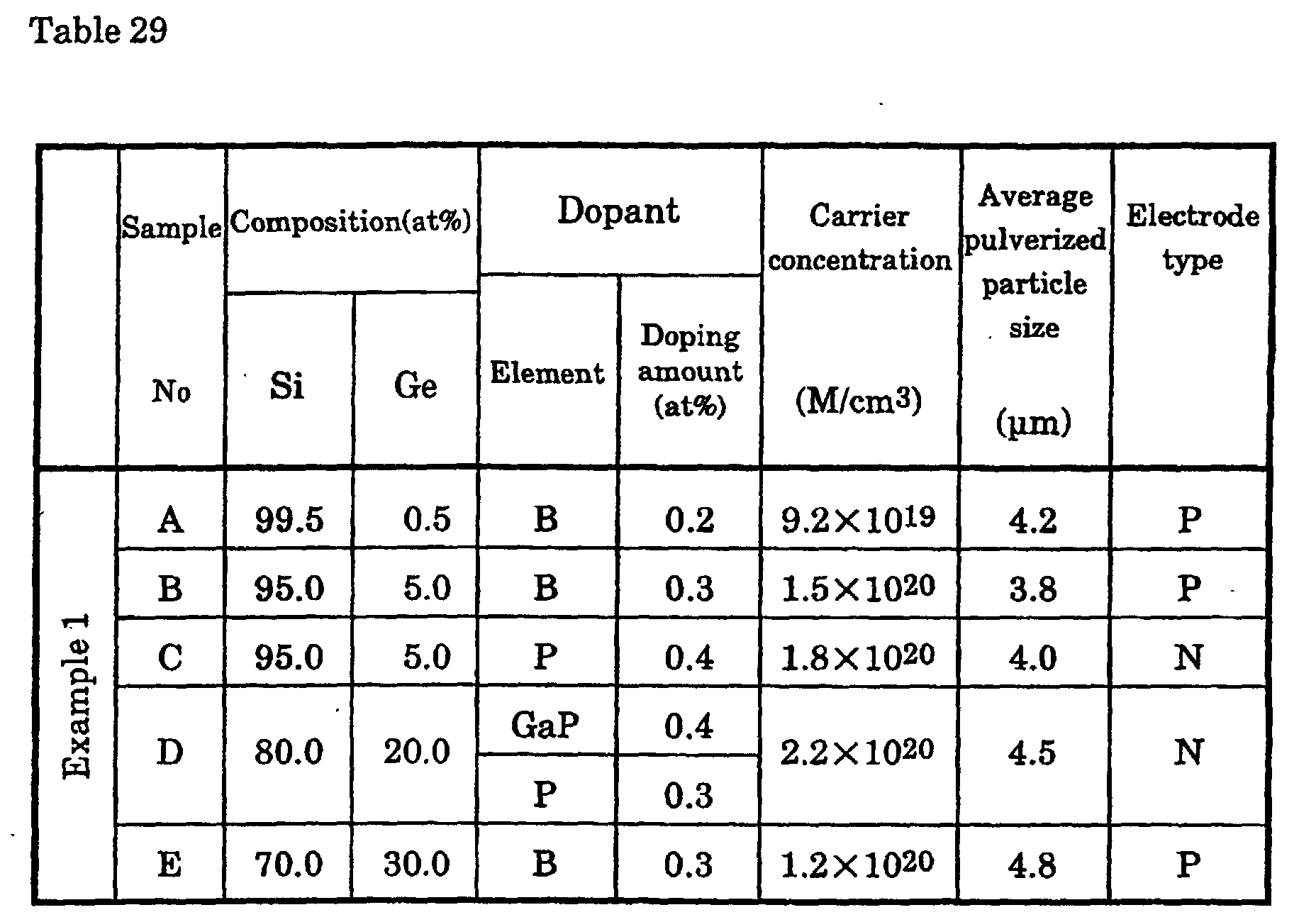
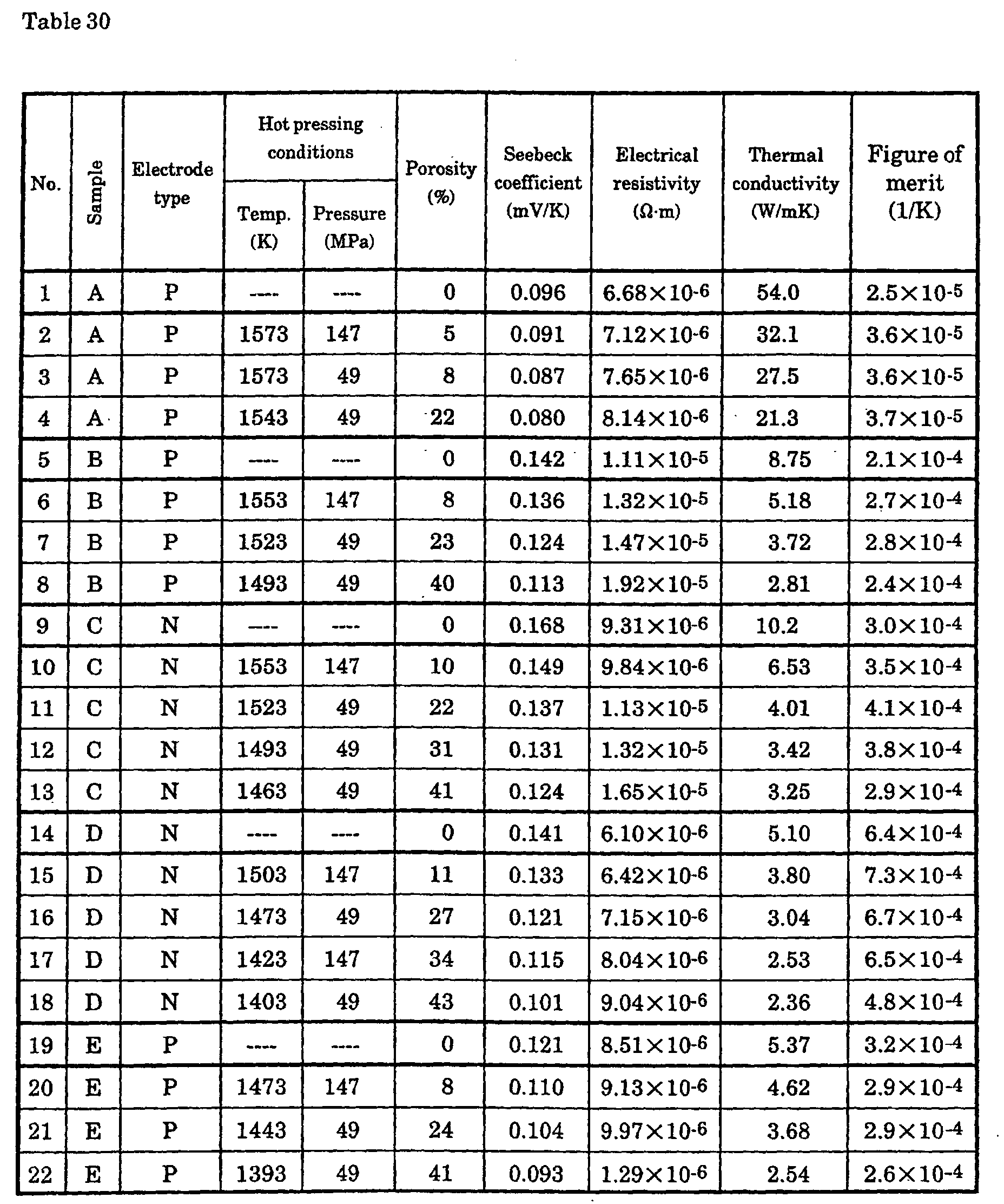
The inventors employed the following process to produce a p-type
Si-Ge semiconductor with controlled porosity. First, one or more transition
metal elements, Group II elements, and Group III elements were added and
melted so that the carrier concentration was 1019 to 1021 (M/m3), and the
resulting ingot was coarsely ground, ground in a disk mill, and ground in a
jet mill. After this, the powder was subjected to hot pressing or discharge
plasma sintering under various molding temperature and pressure
conditions. The thermoelectric conversion characteristics of the
thermoelectric conversion material of a p-type semiconductor with controlled
porosity were measured.
With an Si0.95Ge0.05 p-type semiconductor doped with 0.3 at%
boron, porosity caused no major change in the Seebeck coefficient or
electrical resistance up to a porosity of 40%, but from a porosity of 5%, the
thermal conductivity decreased greatly as porosity increased, and was found
to have dropped to about 30% of that of an arc-melted ingot at a porosity of
40%.
With a p-type semiconductor, at a porosity of less than 5% the
thermal conductivity is virtually the same as that of an ingot, and when the
porosity is over 40%, the Seebeck coefficient decreases and electrical
resistivity increases, the result of which was found to be a decrease in the
Figure of merit. The porosity (X%) here was determined using the formula
(100 ― Y) (%) from the relative density (Y%) of a hot pressed article, where
the density of the ingot is 100%.
Meanwhile, the following process was employed to produce an n-type
silicon-based material with controlled porosity. First, one or more rare
earth elements, Group V elements, and Group VI elements were added and
melted so that the carrier concentration was 1019 to 1021 (M/m3), and the
resulting ingot was coarsely ground, ground in a disk mill, and ground in a
jet mill. After this, the powder was subjected to hot pressing or discharge
plasma sintering under various molding temperature and pressure
conditions. The thermoelectric conversion characteristics of the
thermoelectric conversion material of an n-type semiconductor with
controlled porosity were measured.
With an Si0.95Ge0.05 n-type semiconductor doped with 0.4 at%
phosphorus, just as with the p-type semiconductor, porosity caused no major
change in the Seebeck coefficient or electrical resistance up to a porosity of
40%, but from a porosity of 5%, the thermal conductivity decreased greatly as
porosity increased, and was found to have dropped to about 30% of that of an
arc-melted ingot at a porosity of 40%.
With an n-type semiconductor, at a porosity of less than 5% the
thermal conductivity is virtually the same as that of an ingot, and when the
porosity is over 40%, the Seebeck coefficient decreases and electrical
resistivity increases, the result of which was found to be a decrease in the
Figure of merit.
It is preferable for the hot pressing treatment conditions in the
present invention to comprise a temperature of 1423 to 1573K and a pressure
of 25 to 150 MPa. If the temperature is below 1423K, the porosity of the
sinter will exceed 40%, but partial melting will occur if the temperature is
over 1573K. The pressure should be appropriately selected so as to achieve
the specified porosity.
It is preferable for the discharge plasma sintering conditions in the
present invention to comprise a temperature of 1503 to 1573K and a pressure
of 25 to 150 MPa. If the temperature is below 1503K, the porosity of the
sinter will exceed 40%, but partial melting will occur if the temperature is
over 1573K.
Examples
Example 1
High-purity silicon (10N) and a added element (dopants that
generate carriers are labeled Ap and An, while added elements that do not
generate carriers are labeled Bnc; the same applies to all the added elements
in the following examples) were compounded as shown in Table 1 and then
arc-melted in an argon gas atmosphere to produce p- and n-type silicon
thermoelectric conversion semiconductors. The temperature in the arc
melting was approximately 1900K, and the molten material was cooled at a
rate of 50 to 100K/sec by a water-cooled copper base. The average crystal
grain size of the obtained material was approximately 50 to 100 µm.
The button-shaped ingots thus obtained were cut to sizes of 5 × 5
× 15 mm, 10 × 10 × 2 mm, and 10 (outside diameter) × 2 mm, and the
Seebeck coefficient, Hall coefficient (including carrier concentration and
electrical conductivity), and thermal conductivity were measured for each.
The measurement values at 1100K and the Figure of merit (ZT = S2T/ρκ)
are shown in Table 2.
The temperature differential between the high and low
temperature portions during temperature elevation was set to be about 6K,
the thermoelectromotive force of the samples was measured with a digital
multimeter, and this value was divided by the temperature differential to
find the Seebeck coefficient. The Hall coefficient was measured by AC
method, and the electrical resistance was measured by four-probe method
simultaneously with the carrier concentration. The thermal conductivity
was measured by laser flash method.
Example 2
In order to produce p- and n-type silicon thermoelectric
semiconductors, high-purity silicon (10N) and added elements were
compounded as shown in Table 3, after which this product was put in a
graphite crucible and melted in a high-frequency melting furnace in a
vacuum (10-4 Torr). The melting temperature was approximately 1900K,
the casting temperature was approximately 1800K, and the melt was cast
into a mold with a thickness of 10 mm. The cooling rate of the molten
material was 10 to 50K/sec, and the average crystal grain size of the material
was approximately 100 to 500 µm.
The ingots thus obtained were cut to sizes of 5 × 5 × 15 mm, 10 ×
10 × 2 mm, and 10 (outside diameter) × 2 mm, and the Seebeck coefficient,
Hall coefficient (including carrier concentration and electrical conductivity),
and thermal conductivity of each were measured by the same methods as in
Example 1. Table 4 shows the measured values at 1100K and the Figure of
merit (ZT = S2T/ρκ).
Example 3
In order to produce p- and n-type silicon thermoelectric
semiconductors, high-purity silicon (10N) and added elements were
compounded as shown in Table 5, after which this product was put in a
graphite crucible and melted in a high-frequency melting furnace in a
vacuum (10-4 Torr), and it was confirmed that the components melted
uniformly at approximately 1800K.
After this, the upper part of the above-mentioned graphite crucible
was lowered to 1700K, silicon seed crystals were brought into contact with
the top of the melt, and the melt was slowly pulled up. The inside diameter of
the crucible was 100 mm, the pulling rate was 0.3 to 1 mm/sec, and the pulled
crystals were vibrated once every five seconds in order to render them
polycrystalline. The average crystal grain size of the obtained material was
approximately 1 to 10 µm.
The ingots thus obtained were cut to sizes of 5 × 5 × 15 mm, 10 ×
10 × 2 mm, and 10 (outside diameter) × 2 mm, and the Seebeck coefficient,
Hall coefficient (including carrier concentration and electrical conductivity),
and thermal conductivity of each were measured by the same methods as in
Example 1. Table 6 shows the measured values at 1100K and the Figure of
merit (
ZT = S2T/ρκ).
| No. | Added element Bnc | Doping amount (at%) | Dopant Ap,An | Doping amount (at%) | Melting temp. (K) | Cooling rate (K/sec) | Crystal grain size (µm) |
| 1 | | | B | 0.3 | 1900 | 50 | 100 |
| 2 | | | Al | 1 | 1900 | 50 | 100 |
| 3 | Ge | 3 | B | 0.3 | 1900 | 50 | 100 |
| 4 | Ge | 3 | B | 0.3 | 1900 | 100 | 50 |
| 5 | Ge | 3 | Ga | 1 | 1900 | 50 | 100 |
| 6 | | | P | 1 | 1900 | 50 | 100 |
| 7 | | | As | 1 | 1900 | 50 | 100 |
| 8 | Ge | 3 | P | 1 | 1900 | 50 | 100 |
| 9 | Ge | 3 | P | 1 | 1900 | 100 | 50 |
| 10 | Ge | 3 | Sb | 3 | 1900 | 50 | 100 |
| No. | Seebeck coefficient (mV/K) | Electrical resistivity ×10-5 (Ω·m) | Thermal conductivity (W/m·K) | Figure of merit (ZT) |
| 1 | 0.267 | 1.15 | 37 | 0.18 |
| 2 | 0.231 | 1.24 | 45 | 0.11 |
| 3 | 0.272 | 1.18 | 12 | 0.57 |
| 4 | 0.286 | 1.25 | 9 | 0.80 |
| 5 | 0.291 | 1.37 | 10 | 0.68 |
| 6 | -0.301 | 1.24 | 42 | 0.19 |
| 7 | -0.318 | 1.31 | 48 | 0.18 |
| 8 | -0.305 | 1.28 | 12 | 0.67 |
| 9 | -0.314 | 1.33 | 9 | 0.91 |
| 10 | -0.332 | 1.42 | 10 | 0.85 |
| No. | Added element Bnc | Doping amount (at%) | Dopant Ap,An | Doping amount (at%) | Melting temp. (K) | Cooling rate (K/sec) | Crystal grain size (µm) |
| 11 | | | B | 0.3 | 1900 | 30 | 250 |
| 12 | | | Al | 1 | 1900 | 30 | 250 |
| 13 | Ge | 3 | B | 0.3 | 1900 | 50 | 100 |
| 14 | Ge | 3 | B | 0.3 | 1900 | 30 | 250 |
| 15 | Ge | 3 | B | 0.3 | 1900 | 10 | 500 |
| 16 | Ge | 3 | Ga | 1 | 1900 | 30 | 250 |
| 17 | | | P | 1 | 1900 | 30 | 250 |
| 18 | | | As | 1 | 1900 | 30 | 250 |
| 19 | Ge | 3 | P | 1 | 1900 | 50 | 100 |
| 20 | Ge | 3 | P | 1 | 1900 | 30 | 250 |
| 21 | Ge | 3 | P | 1 | 1900 | 10 | 500 |
| 22 | Ge | 3 | Sb | 3 | 1900 | 30 | 250 |
| No. | Seebeck coefficient (mV/K) | Electrical resistivity ×10-5 (Ω·m) | Thermal conductivity (W/m·K) | Figure of merit (ZT) |
| 11 | 0.272 | 1.08 | 42 | 0.18 |
| 12 | 0.234 | 1.18 | 48 | 0.11 |
| 13 | 0.278 | 1.16 | 14 | 0.52 |
| 14 | 0.280 | 1.12 | 13 | 0.59 |
| 15 | 0.282 | 1.09 | 12 | 0.67 |
| 16 | 0.294 | 1.33 | 12 | 0.60 |
| 17 | -0.309 | 1.20 | 48 | 0.18 |
| 18 | -0.321 | 1.29 | 52 | 0.17 |
| 19 | -0.306 | 1.25 | 14 | 0.59 |
| 20 | -0.309 | 1.21 | 13 | 0.67 |
| 21 | -0.312 | 1.19 | 12 | 0.75 |
| 22 | -0.337 | 1.40 | 12 | 0.74 |
| No. | Added element Bnc | Doping amount (at%) | Dopant Ap,An | Doping amount (at%) | Pulling temp. (K) | Pulling rate (mm/sec) | Crystal grain size (mm) |
| 31 | | | B | 0.3 | 1900 | 0.3 | 3 |
| 32 | | | Al | 1 | 1900 | 0.3 | 3 |
| 33 | Ge | 3 | B | 0.3 | 1900 | 1 | 1 |
| 34 | Ge | 3 | B | 0.3 | 1900 | 0.3 | 3 |
| 35 | Ge | 3 | B | 0.3 | 1900 | 0.1 | 9 |
| 36 | Ge | 3 | Ga | 1 | 1900 | 0.3 | 3 |
| 37 | | | P | 1 | 1900 | 0.3 | 3 |
| 38 | | | As | 1 | 1900 | 0.3 | 3 |
| 39 | Ge | 3 | P | 1 | 1900 | 1 | 1 |
| 40 | Ge | 3 | P | 1 | 1900 | 0.3 | 3 |
| 41 | Ge | 3 | P | 1 | 1900 | 0.1 | 9 |
| 42 | Ge | 3 | Sb | 3 | 1900 | 0.3 | 3 |
| No. | Seebeck coefficient (mV/K) | Electrical resistivity ×10-5 (Ω·m) | Thermal conductivity (W/m·K) | Figure of merit (ZT) |
| 31 | 0.275 | 1.05 | 45 | 0.18 |
| 32 | 0.237 | 1.14 | 51 | 0.11 |
| 33 | 0.280 | 1.19 | 17 | 0.43 |
| 34 | 0.283 | 1.13 | 15 | 0.52 |
| 35 | 0.285 | 1.10 | 14 | 0.58 |
| 36 | 0.298 | 1.30 | 14 | 0.54 |
| 37 | -0.311 | 1.17 | 51 | 0.18 |
| 38 | -0.324 | 1.26 | 54 | 0.17 |
| 39 | -0.309 | 1.22 | 16 | 0.54 |
| 40 | -0.311 | 1.20 | 14 | 0.63 |
| 41 | -0.315 | 1.18 | 13 | 0.71 |
| 42 | -0.339 | 1.38 | 13 | 0.70 |
In order to produce p- and n-type silicon thermoelectric
semiconductors, high-purity silicon (10N) and added elements were
compounded as shown in Table 7, after which this product was put in a
graphite crucible and vacuum melted in a high-frequency melting furnace.
After melting, the material was cast into a mold with a thickness of 10 mm,
and the ingots were ground and then pulverized to an average crystal grain
size of 1 to 50 µm in a stamp mill and a ball mill. The ball mill was a wet type
and made use of a xylene solvent.
The pulverized raw material powder was subjected to hot pressing
in argon for 1 hour at 1325K and 100 MPa to obtain sinters. The sinter
samples thus obtained were cut to sizes of 5 × 5 × 15 mm, 10 × 10 × 2 mm,
and 10 (outside diameter) × 2 mm, and the Seebeck coefficient, Hall
coefficient (including carrier concentration and electrical conductivity), and
thermal conductivity of each were measured. Table 8 shows the measured
values at 1100K and the Figure of merit (ZT = S2T/ρκ).
Example 5
In order to produce p- and n-type silicon thermoelectric
semiconductors, high-purity silicon (10N) and added elements were
compounded as shown in Table 9, after which this product was put in a
graphite crucible and vacuum melted in a high-frequency melting furnace.
After melting, the material was cast into a mold with a thickness of 10 mm to
obtain sheet-form ingots. The ingots were then pulverized, and then finely
pulverized to an average crystal grain size of 1 to 30 µm in a stamp mill and a
jet mill. N2 gas was used in the jet mill, and the pressure was 0.7 MPa.
The finely pulverized raw material powders were compression
molded at a pressure of 200 MPa to sizes of 5 × 5 × 15 mm, 10 × 10 × 2 mm,
and 10 (outside diameter) × 2 mm, and these products were sintered in a
vacuum for 5 hours at 1325K. The Seebeck coefficient, Hall coefficient
(including carrier concentration and electrical conductivity), and thermal
conductivity of each of the sinters thus obtained were measured by the same
methods as in Example 4. Table 10 shows the measured values at 1100K and
the Figure of merit (ZT = S2T/ρκ).
Example 6
In order to produce p- and n-type silicon thermoelectric
semiconductors, high-purity silicon (10N) and added elements were
compounded as shown in Table 11, after which this product was put in a
graphite crucible and vacuum melted in a high-frequency melting furnace.
The melts were discharged through a nozzle with an inside diameter of 3
mm, and the melts were quenched by blowing argon gas on them at 3 MPa to
obtain spherical atomized powder particles with an average diameter of 30 to
100 µm. The cooling rate of this atomized powder was 500 to 1000K/sec, and
the average crystal grain size was 1 to 30 µm.
The atomized powders thus obtained were sintered by discharge
plasma in an argon atmosphere. The sintering conditions were 3 minutes at
1325K. The sample sinters were cut to sizes of 5 × 5 × 15 mm, 10 × 10 × 2
mm, and 10 (outside diameter) × 2 mm, and the Seebeck coefficient, Hall
coefficient (including carrier concentration and electrical conductivity), and
thermal conductivity of each were measured by the same methods as in
Example 4. Table 12 shows the measured values at 1100K and the Figure of
merit (
ZT = S2T/ρκ).
| No. | added element Bnc | Doping amount (at%) | Dopant Ap,An | Doping amount (at%) | Pulverization time (h) | Powder particle size (µm) | Sintering temp. (K) | Sintering time (h) |
| 1 | | | B | 0.3 | 20 | 10 | 1325 | 1 |
| 2 | | | Al | 1 | 20 | 10 | 1325 | 1 |
| 3 | Ge | 3 | B | 0.3 | 10 | 30 | 1325 | 1 |
| 4 | Ge | 3 | B | 0.3 | 20 | 10 | 1325 | 1 |
| 5 | Ge | 3 | B | 0.3 | 50 | 3 | 1325 | 1 |
| 6 | Ge | 3 | Ga | 1 | 20 | 10 | 1325 | 1 |
| 7 | | | P | 1 | 20 | 10 | 1325 | 1 |
| 8 | | | As | 1 | 20 | 10 | 1325 | 1 |
| 9 | Ge | 3 | P | 1 | 10 | 30 | 1325 | 1 |
| 10 | Ge | 3 | P | 1 | 20 | 10 | 1325 | 1 |
| 11 | Ge | 3 | P | 1 | 50 | 3 | 1325 | 1 |
| 12 | Ge | 3 | Sb | 3 | 20 | 10 | 1325 | 1 |
| No. | Seebeck coefficient (mV/K) | Electrical resistivity ×10-5 (Ω·m) | Thermal conductivity (W/m·K) | Figure of merit (ZT) |
| 1 | 0.267 | 1.27 | 29 | 0.21 |
| 2 | 0.231 | 1.31 | 31 | 0.14 |
| 3 | 0.272 | 1.28 | 11 | 0.58 |
| 4 | 0.286 | 1.30 | 9 | 0.72 |
| 5 | 0.283 | 1.33 | 7 | 0.95 |
| 6 | 0.291 | 1.41 | 9 | 0.73 |
| 7 | -0.301 | 1.29 | 30 | 0.26 |
| 8 | -0.318 | 1.34 | 32 | 0.26 |
| 9 | -0.305 | 1.30 | 10 | 0.79 |
| 10 | -0.309 | 1.34 | 9 | 0.87 |
| 11 | -0.314 | 1.37 | 8 | 0.99 |
| 12 | -0.332 | 1.45 | 9 | 0.93 |
| No. | added element Bnc | Doping amount (at%) | Dopant Ap,An | Doping amount (at%) | Raw material supply rate (g/sec) | Powder particle size (µm) | Sintering temp. (K) | Sintering time (h) |
| 21 | | | B | 0.3 | 0.5 | 5 | 1300 | 5 |
| 22 | | | Al | 1 | 0.5 | 5 | 1300 | 5 |
| 23 | Ge | 3 | B | 0.3 | 1 | 10 | 1300 | 5 |
| 24 | Ge | 3 | B | 0.3 | 0.5 | 5 | 1300 | 5 |
| 25 | Ge | 3 | B | 0.3 | 0.25 | 3 | 1300 | 5 |
| 26 | Ge | 3 | Ga | 1 | 0.5 | 5 | 1300 | 5 |
| 27 | | | P | 1 | 0.5 | 5 | 1300 | 5 |
| 28 | | | As | 1 | 0.5 | 5 | 1300 | 5 |
| 29 | Ge | 3 | P | 1 | 1 | 10 | 1300 | 5 |
| 30 | Ge | 3 | P | 1 | 0.5 | 5 | 1300 | 5 |
| 31 | Ge | 3 | P | 1 | 0.25 | 3 | 1300 | 5 |
| 32 | Ge | 3 | Sb | 3 | 0.5 | 5 | 1300 | 5 |
| No. | Seebeck coefficient (mV/K) | Electrical resistivity ×10-5 (Ω·m) | Thermal conductivity (W/m·K) | Figure of merit (ZT) |
| 21 | 0.269 | 1.36 | 25 | 0.23 |
| 22 | 0.235 | 1.41 | 29 | 0.15 |
| 23 | 0.274 | 1.39 | 10 | 0.59 |
| 24 | 0.277 | 1.42 | 8 | 0.74 |
| 25 | 0.281 | 1.46 | 6 | 0.99 |
| 26 | 0.294 | 1.53 | 7 | 0.89 |
| 27 | -0.303 | 1.35 | 27 | 0.28 |
| 28 | -0.320 | 1.41 | 29 | 0.28 |
| 29 | -0.309 | 1.42 | 9 | 0.82 |
| 30 | -0.311 | 1.49 | 7 | 1.02 |
| 31 | -0.314 | 1.55 | 6 | 1.17 |
| 32 | -0.336 | 1.60 | 97 | 1.11 |
| No. | added element Bnc | Doping amount (at%) | Dopant Ap,An | Doping amount (at%) | Spray pressure (MPa) | Powder particle size (µm) | Sintering temp. (K) | Sintering time (sec) |
| 41 | | | B | 0.3 | 5 | 50 | 1325 | 180 |
| 42 | | | Al | 1 | 5 | 50 | 1325 | 180 |
| 43 | Ge | 3 | B | 0.3 | 3 | 75 | 1325 | 180 |
| 44 | Ge | 3 | B | 0.3 | 5 | 50 | 1325 | 180 |
| 45 | Ge | 3 | B | 0.3 | 8 | 30 | 1325 | 180 |
| 46 | Ge | 3 | Ga | 1 | 5 | 50 | 1325 | 180 |
| 47 | | | P | 1 | 5 | 50 | 1325 | 180 |
| 48 | | | As | 1 | 5 | 50 | 1325 | 180 |
| 49 | Ge | 3 | P | 1 | 3 | 75 | 1325 | 180 |
| 50 | Ge | 3 | P | 1 | 5 | 50 | 1325 | 180 |
| 51 | Ge | 3 | P | 1 | 8 | 30 | 1325 | 180 |
| 52 | Ge | 3 | Sb | 3 | 5 | 50 | 1325 | 180 |
| No. | Seebeck coefficient (mV/K) | Electrical resistivity ×10-5 (Ω·m) | Thermal conductivity (W/m·K) | Figure of merit (ZT) |
| 41 | 0.271 | 1.40 | 21 | 0.27 |
| 42 | 0.238 | 1.44 | 24 | 0.18 |
| 43 | 0.277 | 1.42 | 9 | 0.66 |
| 44 | 0.279 | 1.46 | 7 | 0.84 |
| 45 | 0.283 | 1.49 | 6 | 0.99 |
| 46 | 0.298 | 1.58 | 7 | 0.88 |
| 47 | -0.306 | 1.39 | 23 | 0.32 |
| 48 | -0.323 | 1.46 | 27 | 0.29 |
| 49 | -0.311 | 1.47 | 9 | 0.80 |
| 50 | -0.314 | 1.53 | 7 | 1.01 |
| 51 | -0.317 | 1.58 | 6 | 1.17 |
| 52 | -0.339 | 1.63 | 7 | 1.11 |
In order to produce mother particles of silicon thermoelectric
semiconductors, high-purity silicon or Si0.97Ge0.03 was put in a graphite
crucible and vacuum melted in a high-frequency melting furnace. After
melting, the material was cast into a mold with a thickness of 10 mm, and
the ingots were ground and then pulverized to an average crystal grain size
of 10 to 50 µm in a stamp mill and a ball mill. The ball mill was a wet type
and made use of a xylene solvent. The ground powder (mother particles) was
put in a vacuum chamber at 10-3 Torr, and the surface of the particles was
coated (film thickness: 10 to 100 nm) with the carrier-generating dopants
shown in Table 13.
The powder thus obtained was subjected to hot pressing in argon
for 1 hour at 1325K and 100 MPa to obtain sinters. The sinter samples were
cut to sizes of 5 × 5 × 15 mm, 10 × 10 × 2 mm, and 10 (outside diameter) ×
2 mm, and the Seebeck coefficient, Hall coefficient (including carrier
concentration and electrical conductivity), and thermal conductivity of each
were measured. Table 14 shows the measured values at 1100K and the
Figure of merit (ZT = S2T/ρκ).
Example 8
In order to produce mother particles of p- and n-type silicon
thermoelectric semiconductors, high-purity silicon or Si0.97Ge0.03 was put in
a graphite crucible and vacuum melted in a high-frequency melting furnace.
After melting, the material was cast into a mold with a thickness of 10 mm to
obtain sheet-form ingots. The ingots were then pulverized, and then finely
pulverized to an average crystal grain size of 1 to 10 µm in a stamp mill and a
jet mill. N2 gas was used in the jet mill, and the pressure was 0.7 MPa.
The powders (mother particles) thus obtained were put in a
vacuum chamber and treated with SiH4 gas or GeH4 gas, and the powders
were coated with dopants that generate carriers, such as boron, aluminum,
gallium, phosphorus, arsenic, and antimony in the film thicknesses shown in
Table 15.
The coated raw material powders were compression molded at a
pressure of 200 MPa to sizes of 5 × 5 × 15 mm, 10 × 10 × 2 mm, and 10
(outside diameter) × 2 mm, and these products were sintered in a vacuum
for 5 hours at 1325K. The Seebeck coefficient, Hall coefficient (including
carrier concentration and electrical conductivity), and thermal conductivity
of each of the sinters thus obtained were measured by the same methods as in
Example 1. Table 16 shows the measured values at 1100K and the Figure of
merit (ZT = S2T/ρκ).
Example 9
In order to produce mother particles of silicon thermoelectric
cemiconductors, high-purity silicon (10N) was put in a graphite crucible and
vacuum melted in a high-frequency melting furnace. The melt was cast into
a mold with a thickness of 10 mm to obtain sheet-form ingots. The ingots
were ground and then finely pulverized to an average crystal grain size of 10
to 50 µm in a stamp mill and a ball mill. The ball mill was a wet type and
made use of a xylene solvent.
Added elements for producing daughter particles forming a
coating around the silicon were compounded as shown in Table 17, after
which the material was put in a graphite crucible and vacuum melted in a
high-frequency melting furnace. The melt discharged through a nozzle with
an inside diameter of 3 mm, and the melts were quenched by blowing argon
gas on them at 3 MPa, resulting in an average diameter of 30 to 100 µm. The
obtained mother particles were coated with the daughter particles by
mechanofusion such that the daughter particles were in a specific weight
ratio.
The coated raw material powders were sintered by discharge
plasma in an argon atmosphere. The sintering conditions were 180 seconds
at 1325K. The sample sinters were cut to sizes of 5 × 5 × 15 mm, 10 × 10 ×
2 mm, and 10 (outside diameter) × 2 mm, and the Seebeck coefficient, Hall
coefficient (including carrier concentration and electrical conductivity), and
thermal conductivity of each were measured by the same methods as in
Example 1. Table 18 shows the measured values at 1100K and the Figure of
merit (
ZT = S2T/ρκ).
| No. | Composition of mother particles | Diameter of mother particles (µm) | Dopant | Coating film thickness (nm) | Sintering temp. (K) | Sintering time (h) |
| 1 | Si | 10 | B | 10 | 1325 | 1 |
| 2 | Si | 30 | B | 30 | 1325 | 1 |
| 3 | Si | 30 | Al | 50 | 1325 | 1 |
| 4 | Si0.97Ge0.03 | 10 | B | 10 | 1325 | 1 |
| 5 | Si0.97Ge0.03 | 30 | B | 30 | 1325 | 1 |
| 6 | Si0.97Ge0.03 | 30 | Ga | 50 | 1325 | 1 |
| 7 | Si | 10 | P | 30 | 1325 | 1 |
| 8 | Si | 30 | P | 60 | 1325 | 1 |
| 9 | Si | 30 | As | 90 | 1325 | 1 |
| 10 | Si0.97Ge0.03 | 10 | P | 30 | 1325 | 1 |
| 11 | Si0.97Ge0.03 | 30 | P | 60 | 1325 | 1 |
| 12 | Si0.97Ge0.03 | 30 | Sb | 90 | 1325 | 1 |
| No. | Seebeck coefficient (mV/K) | Electrical resistivity ×10-5 (Ω·m) | Thermal conductivity (W/m·K) | Figure of merit (ZT) |
| 1 | 0.267 | 1.31 | 29 | 0.21 |
| 2 | 0.259 | 1.28 | 31 | 0.19 |
| 3 | 0.234 | 1.41 | 35 | 0.12 |
| 4 | 0.271 | 1.35 | 9 | 0.66 |
| 5 | 0.269 | 1.33 | 11 | 0.54 |
| 6 | 0.289 | 1.42 | 10 | 0.65 |
| 7 | -0.301 | 1.30 | 30 | 0.26 |
| 8 | -0.299 | 1.28 | 32 | 0.24 |
| 9 | -0.293 | 1.32 | 37 | 0.19 |
| 10 | -0.309 | 1.34 | 9 | 0.87 |
| 11 | -0.306 | 1.30 | 10 | 0.79 |
| 12 | -0.329 | 1.48 | 10 | 0.80 |
| No. | Composition of mother particles | Diameter of mother particles (µm) | Dopant | Coating film thickness (nm) | Sintering temp. (K) | Sintering time (h) |
| 21 | Si | 3 | B | 3 | 1325 | 5 |
| 22 | Si | 10 | B | 10 | 1325 | 5 |
| 23 | Si | 10 | Al | 15 | 1325 | 5 |
| 24 | Si0.97Ge0.03 | 3 | B | 3 | 1325 | 5 |
| 25 | Si0.97Ge0.03 | 10 | B | 10 | 1325 | 5 |
| 26 | Si0.97Ge0.03 | 10 | Ga | 15 | 1325 | 5 |
| 27 | Si | 3 | P | 10 | 1325 | 5 |
| 28 | Si | 10 | P | 20 | 1325 | 5 |
| 29 | Si | 10 | As | 30 | 1325 | 5 |
| 30 | Si0.97Ge0.03 | 3 | P | 10 | 1325 | 5 |
| 31 | Si0.97Ge0.03 | 10 | P | 20 | 1325 | 5 |
| 32 | Si0.97Ge0.03 | 10 | Sb | 30 | 1325 | 5 |
| No. | Seebeck coefficient (mV/K) | Electrical resistivity ×10-5 (Ω·m) | Thermal conductivity (W/m·K) | Figure of merit (ZT) |
| 21 | 0.271 | 1.39 | 24 | 0.24 |
| 22 | 0.262 | 1.31 | 29 | 0.20 |
| 23 | 0.237 | 1.46 | 31 | 0.14 |
| 24 | 0.273 | 1.40 | 8 | 0.73 |
| 25 | 0.271 | 1.37 | 10 | 0.59 |
| 26 | 0.291 | 1.46 | 10 | 0.64 |
| 27 | -0.303 | 1.35 | 26 | 0.29 |
| 28 | -0.301 | 1.32 | 29 | 0.26 |
| 29 | -0.295 | 1.37 | 32 | 0.22 |
| 30 | -0.311 | 1.39 | 8 | 0.96 |
| 31 | -0.309 | 1.36 | 9 | 0.86 |
| 32 | -0.331 | 1.52 | 9 | 0.88 |
| No. | Composition of mother particles | Diameter of mother particles (µm) | Composition of daughter particles | Diameter of daughter particles (µm) | Sintering temp. (K) | Sintering time ( sec) |
| 41 | Si | 10 | B | 1 | 1325 | 180 |
| 42 | Si | 30 | B | 3 | 1325 | 180 |
| 43 | Si | 30 | Al | 3 | 1325 | 180 |
| 44 | Si | 10 | Ge0.9B0.1 | 1 | 1325 | 180 |
| 45 | Si | 30 | Ge0.9B0.1 | 3 | 1325 | 180 |
| 46 | Si | 30 | Ge0.9Ga0.1 | 3 | 1325 | 180 |
| 47 | Si | 10 | P | 1 | 1325 | 180 |
| 48 | Si | 30 | P | 3 | 1325 | 180 |
| 49 | Si | 30 | As | 3 | 1325 | 180 |
| 50 | Si | 10 | Ge0.8P0.2 | 1 | 1325 | 180 |
| 51 | Si | 30 | Ge0.8P0.2 | 3 | 1325 | 180 |
| 52 | Si | 30 | Ge0.8Sb0.2 | 3 | 1325 | 180 |
| No. | Seebeck coefficient (mV/K) | Electrical resistivity ×10-5 (Ω·m) | Thermal conductivity (W/m·K) | Figure of merit (ZT) |
| 41 | 0.273 | 1.40 | 28 | 0.21 |
| 42 | 0.265 | 1.33 | 31 | 0.19 |
| 43 | 0.240 | 1.49 | 33 | 0.13 |
| 44 | 0.275 | 1.42 | 9 | 0.65 |
| 45 | 0.274 | 1.39 | 10 | 0.59 |
| 46 | 0.294 | 1.48 | 10 | 0.64 |
| 47 | -0.304 | 1.37 | 28 | 0.27 |
| 48 | -0.302 | 1.35 | 30 | 0.25 |
| 49 | -0.297 | 1.39 | 33 | 0.21 |
| 50 | -0.314 | 1.41 | 9 | 0.85 |
| 51 | -0.312 | 1.39 | 10 | 0.77 |
| 52 | -0.333 | 1.54 | 10 | 0.79 |
A silicon (111) wafer was put in a vacuum chamber at 10-6 Torr,
the added elements shown in Table 19 were formed by electron beam heating
alternately as layer A and layer B for 50 laminations in the thicknesses
shown in Table 19.
The samples on the silicon wafers thus obtained were cut to sizes of
5 × 15 mm, 10 × 10 mm, and 10 mm (outside diameter), and the Seebeck
coefficient, Hall coefficient (including carrier concentration and electrical
conductivity), and thermal conductivity of each were measured along with
the silicon wafer. Table 20 shows the measured values at 1100K and the
Figure of merit (ZT = S2T/ρκ).
The temperature differential between the high and low
temperature portions during temperature elevation was set to be about 6K,
the thermoelectromotive force of the samples was measured with a digital
multimeter, and this value was divided by the temperature differential to
find the Seebeck coefficient. The Hall coefficient was measured by AC
method, and the electrical resistance was measured by four-probe method
simultaneously with the carrier concentration. The thermal conductivity
was measured by laser flash method.
Example 11
A silicon (111) wafer was put in a vacuum chamber at 10-2 Torr,
the added elements shown in Table 21 were formed by sputtering alternately
as layer A and layer B for 50 laminations in the thicknesses shown in Table
21.
The samples on the silicon wafers thus obtained were cut to sizes of
5 × 15 mm, 10 × 10 mm, and 10 mm (outside diameter), and the Seebeck
coefficient, Hall coefficient (including carrier concentration and electrical
conductivity), and thermal conductivity of each were measured along with
the silicon wafer. Table 22 shows the measured values at 1100K and the
Figure of merit (
ZT = S2T/ρκ).
| No. | Composition of layer A | Layer A thickness (nm) | Composition of layer B | Layer B thickness (nm) | Cycles (times) | Heating temp. (K) | Heating time (h) |
| 1 | Si | 20 | B | 1 | 50 | 873 | 1 |
| 2 | Si | 50 | B | 3 | 50 | 873 | 1 |
| 3 | Si | 50 | Al | 3 | 50 | 873 | 1 |
| 4 | Si | 20 | Ge0.9B0.1 | 1 | 50 | 873 | 1 |
| 5 | Si | 50 | Ge0.9B0.1 | 3 | 50 | 873 | 1 |
| 6 | Si | 50 | Ge0.8Ga0.2 | 3 | 50 | 873 | 1 |
| 7 | Si | 20 | P | 2 | 50 | 873 | 1 |
| 8 | Si | 50 | P | 5 | 50 | 873 | 1 |
| 9 | Si | 50 | As | 5 | 50 | 873 | 1 |
| 10 | Si | 20 | Ge0.8P0.2 | 2 | 50 | 873 | 1 |
| 11 | Si | 50 | Ge0.8P0.2 | 5 | 50 | 873 | 1 |
| 12 | Si | 50 | Ge0.8Sb0.2 | 5 | 50 | 873 | 1 |
| No. | Seebeck coefficient (mV/K) | Electrical resistivity ×10-5 (Ω·m) | Thermal conductivity (W/m·K) | Figure of merit (ZT) |
| 1 | 0.273 | 1.51 | 21 | 0.26 |
| 2 | 0.264 | 1.47 | 24 | 0.22 |
| 3 | 0.241 | 1.75 | 29 | 0.13 |
| 4 | 0.278 | 1.59 | 7 | 0.76 |
| 5 | 0.276 | 1.49 | 8 | 0.70 |
| 6 | 0.295 | 1.82 | 8 | 0.66 |
| 7 | -0.309 | 1.62 | 19 | 0.34 |
| 8 | -0.306 | 1.53 | 21 | 0.32 |
| 9 | -0.300 | 1.64 | 28 | 0.22 |
| 10 | -0.316 | 1.57 | 7 | 1.00 |
| 11 | -0.312 | 1.53 | 8 | 0.87 |
| 12 | -0.334 | 1.67 | 8 | 0.92 |
| No. | Composition of layer A | Layer A thickness (nm) | Composition of layer B | Layer B thickness (nm) | Cycles (times) | Heating temp. (K) | Heating time (h) |
| 21 | Si | 20 | B | 1 | 50 | 873 | 1 |
| 22 | Si | 50 | B | 3 | 50 | 873 | 1 |
| 23 | Si | 50 | Al | 3 | 50 | 873 | 1 |
| 24 | Si0.9Ge0.1 | 20 | B | 1 | 50 | 873 | 1 |
| 25 | Si0.9Ge0.1 | 50 | B | 3 | 50 | 873 | 1 |
| 26 | Si0.9Ge0.1 | 50 | Ga | 3 | 50 | 873 | 1 |
| 27 | Si | 20 | P | 2 | 50 | 873 | 1 |
| 28 | Si | 50 | P | 5 | 50 | 873 | 1 |
| 29 | Si | 50 | As | 5 | 50 | 873 | 1 |
| 30 | Si0.9Ge0.1 | 20 | P | 2 | 50 | 873 | 1 |
| 31 | Si0.9Ge0.1 | 50 | P | 5 | 50 | 873 | 1 |
| 32 | Si0.9Ge0.1 | 50 | Sb | 5 | 50 | 873 | 1 |
| No. | Seebeck coefficient (mV/K) | Electrical resistivity ×10-5 (Ω·m) | Thermal conductivity (W/m·K) | Figure of merit (ZT) |
| 21 | 0.269 | 1.41 | 23 | 0.25 |
| 22 | 0.261 | 1.37 | 25 | 0.22 |
| 23 | 0.237 | 1.64 | 30 | 0.13 |
| 24 | 0.272 | 1.49 | 8 | 0.68 |
| 25 | 0.270 | 1.40 | 9 | 0.64 |
| 26 | 0.290 | 1.72 | 9 | 0.60 |
| 27 | -0.301 | 1.52 | 21 | 0.31 |
| 28 | -0.299 | 1.43 | 23 | 0.30 |
| 29 | -0.294 | 1.54 | 29 | 0.21 |
| 30 | -0.311 | 1.47 | 8 | 0.90 |
| 31 | -0.306 | 1.43 | 9 | 0.80 |
| 32 | -0.328 | 1.57 | 9 | 0.84 |
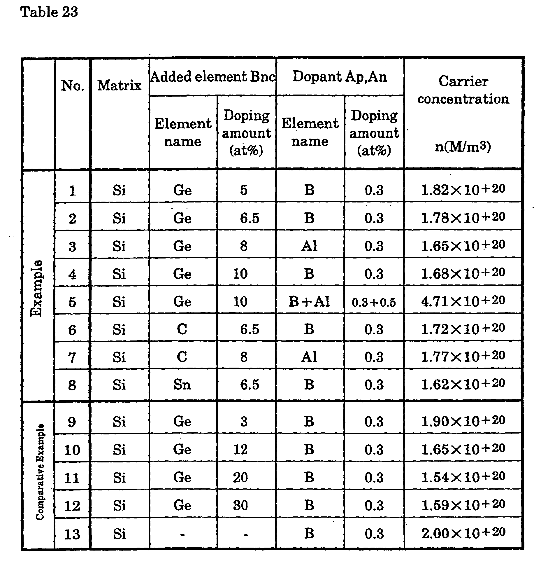
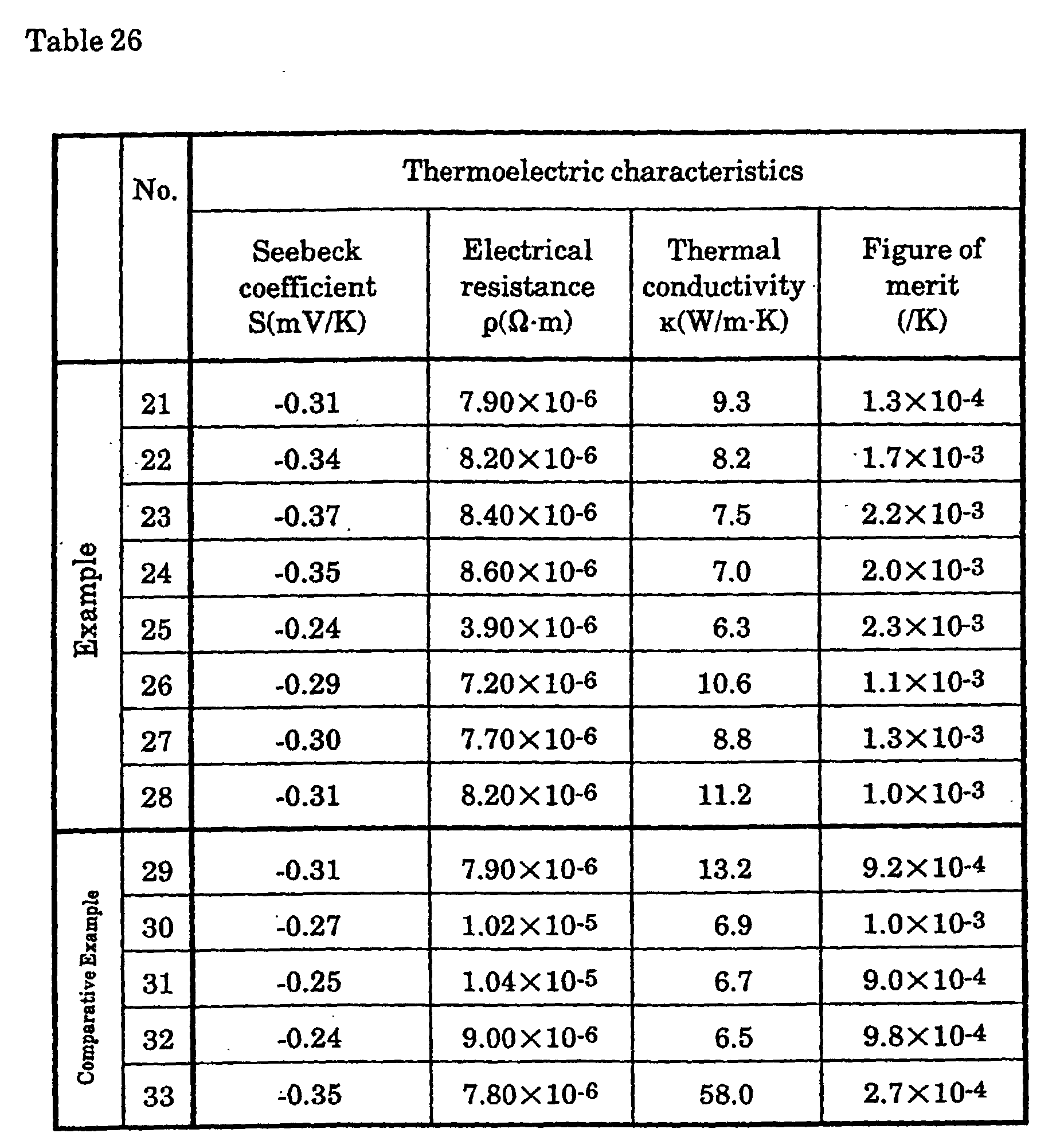
In order to produce a p-type silicon thermoelectric semiconductor,
high-purity silicon (10N), a Group IV element (germanium, carbon, or tin,
the added element Bnc that does not generate carriers), and a Group III
element (the dopant Ap or An that does generate carriers) were compounded
as shown in Table 23, after which they were arc melted in an argon gas
atmosphere. The button-shaped ingots thus obtained were cut to sizes of 5 ×
5 × 15 mm, 10 × 10 × 2 mm, and 10 (diameter) × 2 mm, and the Seebeck
coefficient (S), Hall coefficient (including the carrier concentration (n) and
electrical conductivity (ρ)), and thermal conductivity (κ) were measured for
each.
The temperature differential between the high and low
temperature portions was set to 6K, the thermoelectromotive force of the p-type
semiconductors in which the average temperature between the high and
low temperature portions was 200°C(473K) was measured with a digital
multimeter, and this value was divided by the temperature differential (6K)
to find the Seebeck coefficient. The Hall coefficient was measured by
applying an AC magnetic field of 0.4T at 473K, and the electrical resistance
was measured by four-probe method simultaneously with the carrier
concentration. The thermal conductivity was measured at 473K by laser
flash method.
Tables 23 and 24 show the obtained measurement values and the
Figure of merit (Z = S2/ρκ). The measurement values of an Si-Ge alloy
(containing 30 at% germanium) and of silicon not doped with germanium are
also shown as comparative examples.
Example 13
In order to produce an n-type silicon thermoelectric semiconductor,
high-purity silicon (10N), a Group IV element (germanium, carbon, or tin,
the added element Bnc that does not generate carriers), and a Group V
element (the dopant Ap or An that does generate carriers) were compounded
as shown in Table 24, after which they were arc melted in an argon gas
atmosphere. The button-shaped ingots thus obtained were cut to sizes of 5 ×
5 × 5 mm, 10 × 10 × 2 mm, and 10 (diameter) × 2 mm.
The Seebeck coefficient (S), Hall coefficient (including the carrier
concentration (n) and electrical conductivity (ρ)), and thermal conductivity
(κ) were measured for each in the same manner as in Example 1. Tables 25
and 26 show the obtained measurement values and the Figure of merit (Z =
S2/ρκ). As a comparative material, measurement values are also given for
an Si-Ge alloy (30 at% germanium) and silicon to which no germanium was
added.
Example 14
In order to produce p- and n-type silicon thermoelectric
semiconductors, high-purity silicon (10N), a Group IV element (germanium,
carbon, or tin, the added element Bnc1 that does not generate carriers), a
Group III-V compound semiconductor (GaP, GaAs) or a Group II-VI
compound semiconductor (ZnS) (the compound semiconductor is the added
element Bnc2 that does not generate carriers), and a Group II element and
Group III element, or a Group V element and Group VI element that do
generate carriers were compounded as shown in Table 25, after which they
were melted in a high-frequency melting furnace in a 40 kPa argon gas
atmosphere.
The ingots thus obtained were cut to sizes of 5 × 5 × 5 mm, 10 ×
10 × 2 mm, and 10 (diameter) × 2 mm. The Seebeck coefficient (S), Hall
coefficient (including the carrier concentration (n) and electrical
conductivity (ρ)), and thermal conductivity (K) were measured for each.
Tables 27 and 28 show the obtained measurement values and the Figure of
merit (
Z = S2/ρκ). As a comparative material, measurement values are also
given for an Si-Ge alloy (6.5 at% germanium) to which no Group III-V
compound semiconductor or Group II-VI compound semiconductor was
added.
In order to produce a p-type silicon thermoelectric semiconductor,
high-purity silicon (10N), germanium, and a dopant that generates carriers
were weighed out in the specific proportions shown in Table 29, after which
they were arc melted in an argon gas atmosphere. The button-shaped ingots
thus obtained were coarsely ground, then ground in a disk mill, then ground
in a jet mill to produce powders with the average particle sizes shown in
Table 29.
After this, the hot pressing conditions shown in Table 30 were
maintained for 1 hour to produce sinters having the various porosities shown
in Table 30. The discharge plasma sintering conditions shown in Table 31
were then maintained for 3 minutes to produce sinters having the various
porosities shown in Table 31. An SPS-2040 made by IzumiTech Ltd. was
used for the discharge plasma sintering apparatus.
The sinters thus obtained were cut to sizes of 5 × 5 × 5 mm, 10 ×
10 × 2 mm, and 10 (outside diameter) × 2 mm to produce samples for
measuring the Seebeck coefficient, Hall coefficient (including the carrier
concentration and electrical conductivity), and thermal conductivity of each.
Using platinum for both the electrode in the high temperature
portion and the electrode in the low temperature portion, the temperature
differential between these electrodes was set to 6K, the thermoelectromotive
force of the p-type semiconductors in which the average temperature
between the high and low temperature portions was 323K was measured,
and this thermoelectromotive force was divided by 6K to find the Seebeck
coefficient.
The Hall coefficient was measured by AC method at 323K, and the
electrical resistivity was also measured by four-probe method at that time.
The thermal conductivity was measured at 323K by laser flash method.
These measurement results are given in Tables 30 and 31.
Silicon, the main component of the thermoelectric conversion
material of the present invention, is an outstanding material in terms of
protecting the global environment and conserving the earth's resources, and
also affords excellent safety. Furthermore, it is light (has a low specific
gravity), which makes it very favorable for thermoelectric conversion
elements used in automobiles. Bulk silicon also has good corrosion
resistance, which is an advantage in that no surface treatment or the like is
needed.
Because it makes use of silicon as its main component, the
thermoelectric conversion material of the present invention is less expensive
than Si-Ge-based materials containing large quantities of costly germanium,
and provides a higher Figure of merit than Fe-Si-based materials.
Furthermore, the silicon used in the present invention is much lower in
purity than that used in semiconductor devices, so the raw material is
available at relatively low cost, the result of which is a thermoelectric
conversion material with good productivity, stable quality, and low cost.
The thermoelectric conversion material of the present invention
takes full advantage of the characteristics of silicon, namely, its low
electrical resistance and large Seebeck coefficient despite having a large
carrier concentration, and also greatly ameliorates its drawback of high
thermal conductivity, and is therefore an effective way to obtain a material
with a high Figure of merit. Another advantage is that the properties can be
controlled by means of the type and amount of added elements.
As is clear from the examples, the thermoelectric conversion
material of the present invention containing 5 to 10 at% of at least one of
germanium, carbon, and tin has a Seebeck coefficient of ±2.0 to 4.0 × 10⁻⁴
V/K, which means that the thermal conductivity of this novel silicon-based
thermoelectric conversion can be greatly decreased to less than 50 W/m·K
and the Figure of merit markedly enhanced without decreasing the Seebeck
coefficient originally had by the material.
Also, as is clear from the examples, the thermoelectric conversion
material of the present invention with a porosity of 5 to 40% has a Seebeck
coefficient of 0.07 to 0.200mV/K, which means that the thermal conductivity
of this novel silicon-based thermoelectric conversion can be greatly
decreased to less than 33 W/m·K and the Figure of merit markedly
enhanced without decreasing the Seebeck coefficient originally had by the
material.