EP1083603B1 - Power semiconductor module - Google Patents
Power semiconductor module Download PDFInfo
- Publication number
- EP1083603B1 EP1083603B1 EP00118296A EP00118296A EP1083603B1 EP 1083603 B1 EP1083603 B1 EP 1083603B1 EP 00118296 A EP00118296 A EP 00118296A EP 00118296 A EP00118296 A EP 00118296A EP 1083603 B1 EP1083603 B1 EP 1083603B1
- Authority
- EP
- European Patent Office
- Prior art keywords
- power semiconductor
- semiconductor module
- contact
- module according
- elements
- Prior art date
- Legal status (The legal status is an assumption and is not a legal conclusion. Google has not performed a legal analysis and makes no representation as to the accuracy of the status listed.)
- Expired - Lifetime
Links
Images


Classifications
-
- H—ELECTRICITY
- H01—ELECTRIC ELEMENTS
- H01L—SEMICONDUCTOR DEVICES NOT COVERED BY CLASS H10
- H01L25/00—Assemblies consisting of a plurality of individual semiconductor or other solid state devices ; Multistep manufacturing processes thereof
- H01L25/03—Assemblies consisting of a plurality of individual semiconductor or other solid state devices ; Multistep manufacturing processes thereof all the devices being of a type provided for in the same subgroup of groups H01L27/00 - H01L33/00, or in a single subclass of H10K, H10N, e.g. assemblies of rectifier diodes
- H01L25/04—Assemblies consisting of a plurality of individual semiconductor or other solid state devices ; Multistep manufacturing processes thereof all the devices being of a type provided for in the same subgroup of groups H01L27/00 - H01L33/00, or in a single subclass of H10K, H10N, e.g. assemblies of rectifier diodes the devices not having separate containers
- H01L25/07—Assemblies consisting of a plurality of individual semiconductor or other solid state devices ; Multistep manufacturing processes thereof all the devices being of a type provided for in the same subgroup of groups H01L27/00 - H01L33/00, or in a single subclass of H10K, H10N, e.g. assemblies of rectifier diodes the devices not having separate containers the devices being of a type provided for in group H01L29/00
- H01L25/072—Assemblies consisting of a plurality of individual semiconductor or other solid state devices ; Multistep manufacturing processes thereof all the devices being of a type provided for in the same subgroup of groups H01L27/00 - H01L33/00, or in a single subclass of H10K, H10N, e.g. assemblies of rectifier diodes the devices not having separate containers the devices being of a type provided for in group H01L29/00 the devices being arranged next to each other
-
- H—ELECTRICITY
- H01—ELECTRIC ELEMENTS
- H01L—SEMICONDUCTOR DEVICES NOT COVERED BY CLASS H10
- H01L2924/00—Indexing scheme for arrangements or methods for connecting or disconnecting semiconductor or solid-state bodies as covered by H01L24/00
- H01L2924/0001—Technical content checked by a classifier
- H01L2924/00011—Not relevant to the scope of the group, the symbol of which is combined with the symbol of this group
-
- H—ELECTRICITY
- H01—ELECTRIC ELEMENTS
- H01L—SEMICONDUCTOR DEVICES NOT COVERED BY CLASS H10
- H01L2924/00—Indexing scheme for arrangements or methods for connecting or disconnecting semiconductor or solid-state bodies as covered by H01L24/00
- H01L2924/0001—Technical content checked by a classifier
- H01L2924/00014—Technical content checked by a classifier the subject-matter covered by the group, the symbol of which is combined with the symbol of this group, being disclosed without further technical details
-
- H—ELECTRICITY
- H01—ELECTRIC ELEMENTS
- H01L—SEMICONDUCTOR DEVICES NOT COVERED BY CLASS H10
- H01L2924/00—Indexing scheme for arrangements or methods for connecting or disconnecting semiconductor or solid-state bodies as covered by H01L24/00
- H01L2924/30—Technical effects
- H01L2924/301—Electrical effects
- H01L2924/30107—Inductance
Definitions
- the invention relates to a power semiconductor module with a Base plate on which at least one equipped with power semiconductor chips Substrate is arranged, which can be pressed against the base plate via pressure elements is.
- the power semiconductors or power semiconductor chips from the basic or Insulate the heat sink, which is used for heat dissipation; find this widely used ceramic insulators in disk form with a metallized surface, e.g. Direct copper bonding (DCB) substrates, application on one of which Surface essentially the power semiconductor chips are arranged while the other surface is thermally coupled to the heat sink.
- DCB Direct copper bonding
- circuit breakers are housed in a common housing, what the assembly technically by reducing the number of components simplified, such as in view of a three-phase bridge circuit for three-phase unidirectional or alternating direction that becomes apparent instead of up to six controllable and six non-controllable circuit breakers in the Execution as individual components from just a single component can exist.
- Examples of power semiconductor modules are widely known, cf. e.g. EP-A-0 265 833, EP 0 277 546B1.
- conductive connectors soldered onto the DCB substrate for example tabs, conductive connectors pressed onto the DCB substrate, in particular Pressure contacts, and in an additional insulator, e.g. a case frame, located conductive connector used to which the electrical connection for example by wire bonding, which is one of these processes previous installation of the insulator.
- thermal coupling to the cooling medium - typically over the underside of the component - forms on a module with a DCB base - see. DE35 21 572A1 - the surface of the DCB ceramic that is not occupied by the chips the bottom of the device.
- the thermal coupling is in the Usually by pressing on a typically metallic heat sink produced by a cooling medium, such as air or cooling liquid, heat is withdrawn, the interface between the DCB bottom and the heat sink advantageously with an intermediate layer made of a thermally bonding Medium, e.g. Thermal grease to be provided.
- the one not used by the chips is used Surface of the DCB ceramic with a usually made of a metal or Composite existing base plate thermally coupled; the coupling can by pressing - cf. DE41 31 200C2, DE41 11 247C2 and DE 41 22 428C2 typically in turn using a thermally bonding Medium, e.g. Thermal paste, by soldering - cf. DE43 38 107C1 - or through other coherent connections, the latter in particular with floor slabs Composites are manufactured.
- the bottom plate in turn is then cooled, which can happen, for example, by pressing on one Heatsink or by flow with a cooling medium, such as air or Coolant, provided a suitable geometric Layout.
- Power semiconductor modules according to State of the art in the described embodiments contradict each other such higher integration insofar as they as closed units with own housing, which are based on requirements such as mechanical stability takes up more volume than with higher integration would be required; this fact is both from the point of view of Cost and space economy as well as in terms of electrical behavior, et al influenced by parasitic lead inductances, disadvantageous; too will the accessibility, for example, to those in the power semiconductor module existing electrical potentials through the housing, which makes it difficult not insignificant design effort to connect the module may require.
- Power semiconductor modules are often characterized by complex Constructions from: So in DE4 131 200C2 a structure with a special designed bridge element.
- a semiconductor unit which has a base plate with a substrate that is equipped with a semiconductor chip.
- the contacting of the semiconductor chip takes place via conductive and flexible power connection elements, which are attached to an outer frame.
- the disadvantage is that the reduction in Dimensions of the module due to the height of the spring-loaded Connection elements are limited.
- the object of the invention is to provide a power semiconductor module to create the type mentioned, its structure depending on the application to the essential Parts is reduced and its integrability into a peripheral device, for example a Control device, is nevertheless promoted.
- a peripheral device for example a Control device
- the greatest possible space economy as well as optimal accessibility of the electrical potentials and thermal Resistance of the connections can be guaranteed.
- what should be created Module can be produced economically by simple manufacturing processes and parts as well by using standard components even more flexibility for offer application-specific customization.
- the pressure elements have elastic and conductive contact cords, which between contact rails and substrates are arranged, the contact cords having an elastic core and have an electrically conductive covering.
- the contact cords are both held down by relatively strong pressure elements against this as well as against that on the opposite side of the contact cords arranged metallizations of the substrates pressed. In this way, one reliable permanent electrical connection between the metallizations of the Substrates with which the semiconductor chips are electrically connected, and the Pressure elements reached via the contact cords; also press the Contact cords the substrates against the one on the opposite side Base plate, so that a favorable heat transfer between the substrates with the to cooling semiconductor chips and the cooled base plate is achieved.
- the arrangement and development of the contact cords according to the invention creates at the same time the prerequisite for an advantageous training of the overall structure of the power semiconductor module according to the invention in the direction of a comparatively simple production, also for different application and Applications. It is characterized by the fact that there are fields on the base plate defining frame can be fixed by means of centering elements, at least some of the fields correspond to substrates using power semiconductor chips are equipped.
- This inventive design of a power semiconductor module gives defined positions for the substrates with the semiconductor chips on them in front. In adaptation to different needs it is possible to all or to cover individual fields with substrates and then to contact them. A change in the tools for making the frame for different applications are therefore not required.
- the contacting of the Chips and the entire production of the power semiconductor module according to the invention improved if on the centering elements and the contact and Counter rails pressure bracket are provided.
- the pressure bracket can be approx Match length and width with the counter rails.
- the frame is grid-shaped and the grid of the Frame integrally formed with it guides for auxiliary contacts. These are thus in one operation together with the frame, in particular manufactured by injection molding.
- the guides are electrical Contacts can be inserted, e.g. connect to one on the Power semiconductor module according to the invention arranged circuit board manufacture, which in turn is an interface to an additional unit, e.g. one Control unit, forms.
- a power semiconductor module 10 according to the invention is described in the following Order of assembly of an exemplary three-phase controlled Bridge circuit explained:
- the base plate 1 is in usually the base plate of a control unit, not shown form, the further, especially electronic assemblies, and in finished design can be closed by additional housing parts.
- the typically metallic base plate 1 can be cooled, e.g. by Air also flows onto cooling fins (not shown) or flows through them Integrated channels with coolant, not specifically shown. If necessary can on the base plate 1 in the area between the threaded bolt 2 Heat transfer to those to be pressed in a later assembly step Medium that improves substrates - e.g. Thermal compound - to be applied.
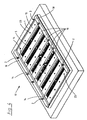
- Fig. 1 also shows a frame placed on the base plate 1 or Housing frame 3. It is, as explained below, in the assembled state of the Power semiconductor module pressed onto the base plate 1. It serves as protection of the power semiconductor chips by the potting compound applied to them prevents it from flowing away, as well as the management of those listed below Components during and partly after assembly. This means that at the Housing frame 3 no special requirements with regard to the recording of forces, so that it is an inexpensive thin-walled plastic part, e.g. made of a thermoset.
- the frame 3 has a circumferential Edge part 4 from a right-angled angle profile; continue a longitudinal web 5 and crossbars 6, which form a grid which defines individual fields 7.
- auxiliary contacts intended at the Longitudinal web 5 are integrally formed guides 8 for auxiliary contacts intended. They have recesses 9 into which these auxiliary contacts be introduced, e.g. for the transmission of control signals to one on the Module to be provided circuit board (not shown).
- the frame 3 has at its on the base plate 1 leg 19, the right angle to the edge part 4 is provided, corresponding to the centering elements 2 Openings so that it can be placed on the base plate 1 and in there the level of the base plate 1 is fixed.
- substrates 13 into the fields 7 of the housing frame 3rd are inserted. These are DCB substrates, as is known, on which the Power semiconductor chips are arranged.
- substrates 13 with different chip configurations - are shown larger chips 11 and smaller chips 12 - without further design changes to use on the structure of the frame 3.
- High efficiency of the manufacturing process is achieved by using identical substrates for all switches.
- the soldered and wire-bonded substrates 13 can during their Manufacturing process can already be checked for errors, so that the installation defective components in the power semiconductor module 10 is to be excluded.
- a plurality of substrates 13 can also be connected in parallel in order to a circuit breaker with a higher number of chips than economical on one Can be realized to build substrate:
- the arrangement shown Three-phase bridge consisting of six switches is with twelve substrates, therefore two of them per switch.
- the substrates 13 correspond in their Dimensions of those of the fields 7, so that during assembly by the Grid of the frame are held reliably.
- counter rails 14 on the Threaded bolt 2 inserted. Their task is also to manage the contact rails 15 to be used for the next assembly step, see FIG. 3 Inclusion of the contact rails 15 and clear fixation are the Counter rails 14 are provided with recesses 16, the cross section of which the Contact rails 15 corresponds to those in the embodiment shown Recesses 16 and the contact rails 15 dimensioned so that they on the Top edge, that is in the area of the exit of the threaded bolts 2 from the Counter rails, flush with the upper edge of the edge part of the frame 3 to lock.
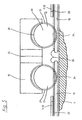
- FIG. 5 is a cross section of a contact rail 15, of contact cords 17th and the substrates 13 contacted therewith.
- the electrical connection on the other hand, the surface pressure of the substrates 13 against the surface heat-dissipating base plate 1 for thermal coupling.
- Advantageous executed contact cords consist of a core 20 made of elastic Material, e.g. Silicone rubber that is conductive and flexible, but not necessarily surrounded by elastic sheath 21, e.g. Copper wire mesh. In this way, one decouples the Features flat pressure - that of which in particular is sufficient heat-resistant elastomer core is applied - and electrical Contacting with the lowest possible resistance and long service life is also carried out in thermal-mechanical cycles.
- the contact cord 17 with its sheath 21 is in the uncompressed state State drawn between the contact rail 15 and the substrate 13 to the compression that occurs during final assembly in the illustration to indicate overlapping areas. In fact, they are in the assembled state Contact cords 17 on the profile 30 of the contact rails 15 and flat on A possible long-term impairment of the chips 11, 12 by Contamination of the encapsulation to be introduced later by the material of the Contact cords 17 can be excluded if an elastomer material, e.g. based on silicone, such as silicone rubber.
- the chips 11, 12 are over a solder layer 22 connected to the substrate 13, which has an electrically conductive copper layer 25
- the layer 24 represents a thermal paste 24, which between Substrate 13 and the base or cooling plate 1 is present.
- contact cords 17 there are preferably two contact cords 17 per contact rail 15. She extend essentially over the length of the contact rails 15, in which further recesses 23 are provided. You can use it to attach one circuit board covering power semiconductor module according to the invention be used.
- the structure mentioned also has an advantageous effect in the construction according to the invention Guide the contact rails 15 in the counter rails 14 from. If push bar 18 are placed on the threaded bolts 2, as shown in Fig. 4, results in by pressing the pressure bracket 18 and counter rails 14 together Stop by means of nuts screwed onto the threaded bolts 2 a constant Contact pressure regardless of the exact torque when tightening, which the Variance of relevant product properties such as electrical and thermal Coupling of the power semiconductors minimized.
- the gate contact springs shown in FIG. 3 and FIG. 4 serve the electrical Connection of control potentials required for controllable switches. she are not burdened with larger currents.
- mechanical Guides 8 are provided in the housing frame, which slide sideways prevent, but otherwise do not absorb mechanical forces.
- a circuit board for example, can be attached in a simple manner to the structure of the power semiconductor module 10 shown in FIG. 4, which is typically done by screwing on using the recesses 23, which can be designed as threaded holes.
- This circuit board can have contact surfaces on its side facing the contact rails, which contact the contact rails on their surface visible in FIG. 4, which contains the recesses 23, by the pressure of the screwing on flat and thus with high current carrying capacity.
- capacitors can be arranged between the positive and negative electrical potential of the intermediate circuit, as are typically used in voltage intermediate circuit converters.
- the construction according to the invention has the particular advantage that the capacitors are located in the immediate vicinity of the semiconductor chips, which, as a low-inductance construction, contributes in particular to optimizing the switching behavior of the semiconductor chips.
- the external connection of the power semiconductor module for example for the external voltage supply and the consumer, typically an electrical machine, can be carried out analogously to the fastening of the printed circuit board using the screw connections already mentioned, which use the recesses 23.
- the control potentials are removed from the substrates 13 by means of contact springs. If a circuit board is attached to the power semiconductor module in the manner described, these contact springs can transmit the control potentials to metallized fields arranged at corresponding locations on the circuit board. This contacting takes place without additional operations during the described mounting of the circuit board.
- the gate drivers will be arranged on the circuit board, which in turn are in the immediate vicinity of the semiconductor chips. This is advantageous both in terms of assembly technology and in terms of electrical behavior.
- the arrangement of the individual components described above results from the connection sequence of the power semiconductor module according to the invention, namely in the case L + , G 1 , L 1 , G 2 , L - , G 4 , L 2 , G 3 shown in FIG. 4 , L + , G 5 , L 3 , G 6 , L - , based on the usual designation scheme for three-phase controlled bridges.
- the pressure bracket 18 can serve as a leading assembly aid when assembling the circuit board.
- a power semiconductor module 10 assembled in this way can already be fully tested, so that components, in particular substrates 13, can still be replaced if necessary. Otherwise, you will continue with partial or complete potting of the power semiconductor module 10 and assembly of the other components of the control unit, the part of which it can form.
- the counter rails 14 and pressure bracket 18 can also be made inexpensive thermosets are manufactured.
Description
Die Erfindung bezieht sich auf ein Leistungshalbleiter-Modul mit einer Grundplatte, auf der mindestens ein mit Leistungshalbleiter-Chips bestücktes Substrat angeordnet ist, das über Druckelemente an die Grundplatte andrückbar ist.The invention relates to a power semiconductor module with a Base plate on which at least one equipped with power semiconductor chips Substrate is arranged, which can be pressed against the base plate via pressure elements is.
Bei der Herstellung von Leistungshalbleiter-Modulen ist es in der Regel erforderlich, die Leistungshalbleiter oder Leistungshalbleiter-Chips vom Grundoder Kühlkörper, der der Wärmeabfuhr dient, elektrisch zu isolieren; hierzu finden weithin keramische Isolatoren in Scheibenform mit metallisierter Oberfläche, z.B. Direct-Copper-Bonding (DCB)-Substrate, Anwendung, auf deren einer Oberfläche im wesentlichen die Leistungshalbleiter-Chips angeordnet sind, während die andere Oberfläche thermisch an den Kühlkörper angekoppelt wird. Die von leistungsstärkeren Anwendungen benötigten Stromtragfähigkeiten der Leistungsschalter werden normalerweise durch Parallelschaltung einzelner Leistungshalbleiter-Chips zu einem Leistungsschalter erreicht. Zusätzlich können mehrere Leistungsschalter in einem gemeinsamen Gehäuse untergebracht werden, was den Aufbau montagetechnisch durch Verminderung der Anzahl der Bauteile vereinfacht, wie beispielsweise angesichts einer dreiphasigen Brückenschaltung für dreiphasige Gleich- oder Wechselrichtung deutlich wird, die anstatt aus bis zu sechs steuerbaren und sechs nicht steuerbaren Leistungsschaltern in der Ausführung als Einzelbauelemente so aus lediglich einem einzigen Bauelement bestehen kann. Beispiele für Leistungshalbleitermodule sind vielfach bekannt, vgl. z.B. EP-A-0 265 833, EP 0 277 546B1. It is usually the case when manufacturing power semiconductor modules required, the power semiconductors or power semiconductor chips from the basic or Insulate the heat sink, which is used for heat dissipation; find this widely used ceramic insulators in disk form with a metallized surface, e.g. Direct copper bonding (DCB) substrates, application on one of which Surface essentially the power semiconductor chips are arranged while the other surface is thermally coupled to the heat sink. The current carrying capacities required by more powerful applications Circuit breakers are normally made by connecting individual ones in parallel Power semiconductor chips reached to a circuit breaker. In addition, you can several circuit breakers are housed in a common housing, what the assembly technically by reducing the number of components simplified, such as in view of a three-phase bridge circuit for three-phase unidirectional or alternating direction that becomes apparent instead of up to six controllable and six non-controllable circuit breakers in the Execution as individual components from just a single component can exist. Examples of power semiconductor modules are widely known, cf. e.g. EP-A-0 265 833, EP 0 277 546B1.
Es sind verschiedene Methoden bekannt, solche Leistungshalbleiter-Module aufzubauen.Various methods are known, such power semiconductor modules build.
Bezüglich elektrischer Verbindung zu den Anschlüssen werden beispielsweise auf das DCB-Substrat aufgelötete leitende Verbinder, insbesondere Laschen, auf das DCB-Substrat aufgepreßte leitende Verbinder, insbesondere Druckkontakte, und in einem zusätzlichen Isolator, z.B. einem Gehäuserahmen, befindliche leitende Verbinder verwendet, zu denen die elektrische Verbindung beispielsweise durch Drahtbonden hergestellt wird, was eine diesem Prozeß vorausgehende Montage des Isolators voraussetzt.With regard to electrical connection to the connections, for example conductive connectors soldered onto the DCB substrate, in particular tabs, conductive connectors pressed onto the DCB substrate, in particular Pressure contacts, and in an additional insulator, e.g. a case frame, located conductive connector used to which the electrical connection for example by wire bonding, which is one of these processes previous installation of the insulator.
Hinsichtlich der thermischen Ankopplung an das Kühlmedium - typischerweise
über die Unterseite des Bauelements - bildet bei einem Modul mit DCB-Boden
- vgl. DE35 21 572A1 - die nicht von den Chips belegte Oberfläche der DCB-Keramik
die Unterseite des Bauelements. Die thermische Kopplung wird in der
Regel durch Anpressen an einen typischerweise metallischen Kühlkörper
hergestellt, dem von einem Kühlmedium, wie Luft oder Kühlflüssigkeit, Wärme
entzogen wird, wobei die Grenzfläche zwischen DCB-Boden und Kühlkörper
vorteilhafterweise mit einer Zwischenlage aus einem thermisch verbindenden
Medium, z.B. Wärmeleitpaste, zu versehen ist.With regard to the thermal coupling to the cooling medium - typically
over the underside of the component - forms on a module with a DCB base
- see.
Bei einem Modul mit Bodenplatte wird die nicht von den Chips belegte
Oberfläche der DCB-Keramik mit einer in der Regel aus einem Metall oder
Verbundwerkstoff bestehenden Bodenplatte thermisch gekoppelt; die Kopplung
kann durch Anpressen - vgl. DE41 31 200C2, DE41 11 247C2 und DE 41 22
428C2 typischerweise wiederum unter Verwendung eines thermisch verbindenden
Mediums, z.B. Wärmeleitpaste, durch Anlöten - vgl. DE43 38 107C1 - oder durch
andere schlüssige Verbindungen, letztere insbesondere bei Bodenplatten aus
Verbundwerkstoffen, hergestellt werden. Die Bodenplatte ihrerseits wird dann
gekühlt, was beispielsweise geschehen kann durch Anpressen an einen
Kühlkörper oder durch Anströmen mit einem Kühlmedium, wie Luft oder
Kühlflüssigkeit, unter der Voraussetzung einer geeigneten geometrischen
Gestaltung.In the case of a module with a base plate, the one not used by the chips is used
Surface of the DCB ceramic with a usually made of a metal or
Composite existing base plate thermally coupled; the coupling
can by pressing - cf. DE41 31 200C2,
Dieser Stand der Technik ist mit einer Reihe von Nachteilen wie folgt behaftet:This prior art has a number of disadvantages as follows:
Leistungshalbleiter-Module dienten ursprünglich, wie oben ausgeführt, der Erhöhung des Integrationsgrades leistungselektronischer Schaltungsanordnungen. Verfolgt man dieses Ziel weiter, so wird es erforderlich, Leistungselektronik zusammen mit peripheren Funktionen wie Ansteuerung, Zwischenkreiskondensatoren u.ä. in ein verbrauchernahes Steuergerät zu integrieren: Für einen Einzelradantrieb mit einem Drehstrommotor könnte ein solches Steuergerät beispielsweise in der Form an das Motorgehäuse angelehnt werden, das gleiche Kühlmedium wie der Motor nutzen und als elektrische Schnittstellen eine Gleichspannungs-Einspeisung sowie einen bidirektionalen Bus zur Informationsübertragung aufweisen. Leistungshalbleitermodule nach dem Stand der Technik in den beschriebenen Ausführungsformen widersetzen sich solcher höheren Integration insofern, als sie als abgeschlossene Einheiten mit eigenem Gehäuse ausgeführt sind, welche aufgrund von Anforderungen wie mechanischer Stabilität mehr Volumen einnimmt, als bei höherer Integration erforderlich wäre; diese Tatsache ist sowohl unter den Gesichtspunkten von Kosten und Raumökonomie wie auch hinsichtlich des elektrischen Verhaltens, u.a. beeinflußt durch parasitäre Zuleitungsinduktivitäten, von Nachteil; auch wird die Zugänglichkeit beispielsweise zu den im Leistungshalbleiter-Modul vorhandenen elektrischen Potentialen durch das Gehäuse erschwert, was einen nicht unerheblichen konstruktiven Aufwand zum Anschluß des Moduls erforderlich machen kann.Power semiconductor modules originally served as described above Increasing the degree of integration of power electronic circuit arrangements. If you continue to pursue this goal, it will become necessary to have power electronics together with peripheral functions such as control, DC link capacitors, etc. into a consumer-related control unit integrate: For a single wheel drive with a three-phase motor one could such control unit, for example, based on the shape of the motor housing be using the same cooling medium as the engine and as electrical Interfaces a direct voltage supply and a bidirectional bus for information transfer. Power semiconductor modules according to State of the art in the described embodiments contradict each other such higher integration insofar as they as closed units with own housing, which are based on requirements such as mechanical stability takes up more volume than with higher integration would be required; this fact is both from the point of view of Cost and space economy as well as in terms of electrical behavior, et al influenced by parasitic lead inductances, disadvantageous; too will the accessibility, for example, to those in the power semiconductor module existing electrical potentials through the housing, which makes it difficult not insignificant design effort to connect the module may require.
Die Zuverlässigkeit der elektrischen Verbindungen, insbesondere bei gelöteten Anschlüssen nach außen, kann durch thermische Ermüdung zu wünschen übrig lassen. Man bemüht sich, dieser Tatsache durch geeignete Gestaltung der Anschlüsse, z.B. mit Dehnungsbögen, oder spezielle Lötverfahren - vgl. z.B. DD 283 236A5 - entgegenzuwirken. Werden die elektrischen Verbindungen hingegen über Druckkontakte mit metallischen Federn hergestellt, so können diese unter durch die Verlustwärme der umgebenden Halbleiter- Chips entstehenden Hitzeeinwirkung weich, d. h. verstärkt plastisch verformbar werden, so daß der Andruck der Substrate nachlassen wird. Weiterhin weisen durch ihre Härte mechanisch günstigere metallische Legierungen oft einen höheren elektrischen Widerstand als auf gutes Leitungsverhalten optimierte Materialien auf. Kontaktfedern, die diese Nachteile vermeiden, sind durch ihre besondere stoffliche Zusammensetzung meist teuer, daher wenig wirtschaftlich einzusetzen. In jedem Falle besteht die Gefahr, daß die Enden der Kontaktfedern bzw. die diesen gegenüberliegenden Kontaktflächen durch Kratzbewegungen bei thermisch bedingter Arbeit des Aufbaus verschlissen werden.The reliability of the electrical connections, especially for soldered ones External connections may be unsatisfactory due to thermal fatigue to let. Efforts are made to ensure that this is done by designing the Connections, e.g. with expansion bends, or special soldering processes - cf. e.g. DD 283 236A5 - to counteract. Will the electrical connections produced on the other hand via pressure contacts with metallic springs, so these can under arising from the heat loss of the surrounding semiconductor chips Heat exposure soft, d. H. are increasingly plastically deformable, so that the Pressure of the substrates will decrease. Furthermore, show by their hardness mechanically cheaper metallic alloys often have a higher electrical Resistance than materials optimized for good conductance. Contact springs that avoid these disadvantages are special due to their Material composition usually expensive, therefore it is not very economical to use. In any case, there is a risk that the ends of the contact springs or these opposite contact surfaces by scratching movements when thermal conditional work of construction.
Die Sicherstellung des Wärmeübergangs ist mit Schwierigkeiten verbunden, konstruktiv aufwendig und häufig nicht über die erforderliche Lebensdauer des Leistungshalbleiter-Moduls gewährleistet: Beschreibung von Schwachstellen sowie Lösungsvorschläge finden sich z.B. in DE39 40 933 - Nachbiegen der belöteten Bodenplatte -, DE43 38 107C1 - Formgebung für Bodenplatte -, DE19 707 514A1 - Einführung von Sollbiegestellen in die Bodenplatte - DE35 08 456A1 - Andrückvorrichtung für das Substrat mittels Justierschrauben und Zwischenstücken- oder DE4 131 200 C2 - Ausübung des Druckes durch Federelemente, was eine Justierung erforderlich machen kann.Ensuring heat transfer is difficult, structurally complex and often not over the required lifetime of the Power semiconductor module ensures: Description of vulnerabilities and suggestions for solutions can be found e.g. in DE39 40 933 - re-bending the soldered base plate -, DE43 38 107C1 - shaping for base plate -, DE19 707 514A1 - introduction of predetermined bending points into the base plate - DE35 08 456A1 - pressing device for the substrate by means of adjusting screws and intermediate pieces - or DE4 131 200 C2 - exertion of pressure by Spring elements, which may require adjustment.
Nach dem Stand der Technik im Druckkontakt-Verfahren aufgebaute Leistungshalbleiter-Module zeichnen sich häufig durch aufwendige Konstruktionen aus: So wird in DE4 131 200C2 ein Aufbau mit einem speziell gestalteten Brückenelement beschrieben. Man erkennt, daß eine solche Konstruktion auf spezielle Schaltungen zugeschnitten sein muß; Schaltungsänderungen führen zu Werkzeugkosten bei entsprechenden Lieferzeiten, was sich angesichts steigender Anforderungen an Preise und Lieferzeiten auch für neue applikationsspezifische Leistungshalbleiter-Module nachteilig auswirkt. Built according to the state of the art in the pressure contact method Power semiconductor modules are often characterized by complex Constructions from: So in DE4 131 200C2 a structure with a special designed bridge element. One recognizes that such Construction must be tailored to special circuits; Circuit changes lead to tool costs for the corresponding ones Delivery times, which in view of increasing demands on prices and Delivery times also for new application-specific power semiconductor modules adversely affects.
Aus der DE-A-36 43 288 ist eine Halbleiterbaueinheit bekannt, die über eine Grundplatte mit einem Substrat verfügt, das mit einem Halbleiterchip bestückt ist. Die Kontaktierung des Halbleiterchips erfolgt über leitfähige und flexible Stromanschlußelemente, die an einem äußeren Rahmen befestigt sind. Nachteilig ist, dass der Reduzierung der Abmessungen des Moduls aufgrund der Bauhöhe der federnd vorgespannten Anschlußelemente Grenzen gesetzt sind.From DE-A-36 43 288 a semiconductor unit is known which has a base plate with a substrate that is equipped with a semiconductor chip. The contacting of the semiconductor chip takes place via conductive and flexible power connection elements, which are attached to an outer frame. The disadvantage is that the reduction in Dimensions of the module due to the height of the spring-loaded Connection elements are limited.
Die Aufgabe der Erfindung besteht darin, ein Leistungshalbleiter-Modul der eingangs genannten Art zu schaffen, dessen Aufbau anwendungsabhängig auf die wesentlichen Teile reduziert ist und dessen Integrierbarkeit in ein Peripheriegerät, beispielsweise ein Steuergerät, dennoch gefördert wird. Hierbei sollen größtmögliche Raumökonomie sowie optimale Zugänglichkeit der elektrischen Potentiale sowie thermische Beständigkeit der Anschlüsse gewährleistet sein. Darüber hinaus soll das zu schaffende Modul durch einfache Fertigungsprozesse und -teile wirtschaftlich herstellbar sein sowie durch Rückgriff auf Standardkomponenten noch zusätzlich höhere Flexibilität für anwendungsspezifische Anpassung bieten.The object of the invention is to provide a power semiconductor module to create the type mentioned, its structure depending on the application to the essential Parts is reduced and its integrability into a peripheral device, for example a Control device, is nevertheless promoted. Here, the greatest possible space economy as well as optimal accessibility of the electrical potentials and thermal Resistance of the connections can be guaranteed. In addition, what should be created Module can be produced economically by simple manufacturing processes and parts as well by using standard components even more flexibility for offer application-specific customization.
Diese Aufgabe ist gemäß der Erfindung dadurch gelöst, dass die Druckelemente elastische und leitfähige Kontaktschnüre aufweisen, welche zwischen Kontaktschienen und Substraten angeordnet sind, wobei die Kontaktschnüre einen elastischen Kern und eine elektrisch leitfähige Umhüllung aufweisen.This object is achieved according to the invention in that the pressure elements have elastic and conductive contact cords, which between contact rails and substrates are arranged, the contact cords having an elastic core and have an electrically conductive covering.
Die Kontaktschnüre werden durch Niederhalten relativ starker Druckelemente sowohl gegen diese als auch gegen die auf der gegenüberliegenden Seite der Kontaktschnüre angeordneten Metallisierungen der Substrate gedrückt. Auf diese Weise wird eine zuverlässige dauerstandfeste elektrische Verbindung zwischen den Metallisierungen der Substrate, mit denen die Halbleiter-Chips elektrisch verbunden sind, und den Druckelementen über die Kontaktschnüre erreicht; außerdem drücken die Kontaktschnüre die Substrate gegen die auf deren entgegengesetzter Seite befindliche Grundplatte, so dass ein günstiger Wärmeübergang zwischen den Substraten mit den zu kühlenden Halbleiter-Chips und der gekühlten Grundplatte erreicht wird.The contact cords are both held down by relatively strong pressure elements against this as well as against that on the opposite side of the contact cords arranged metallizations of the substrates pressed. In this way, one reliable permanent electrical connection between the metallizations of the Substrates with which the semiconductor chips are electrically connected, and the Pressure elements reached via the contact cords; also press the Contact cords the substrates against the one on the opposite side Base plate, so that a favorable heat transfer between the substrates with the to cooling semiconductor chips and the cooled base plate is achieved.
Die erfindungsgemäße Anordnung und Weiterbildung der Kontaktschnüre schafft zugleich die Voraussetzung für eine vorteilhafte Ausbildung des Gesamtaufbaus des erfindungsgemäßen Leistungshalbleiter-Moduls in Richtung auf eine vergleichsweise einfache Fertigung, auch für unterschiedliche Anwendungs- und Einsatzgebiete. Sie ist dadurch gekennzeichnet, daß auf der Grundplatte ein Felder definierender Rahmen mittels Zentrierelementen fixierbar ist, wobei mindestens ein Teil der Felder korrespondierende Substrate, die mit Leistungshalbleiter-Chips bestückt sind, aufnimmt.The arrangement and development of the contact cords according to the invention creates at the same time the prerequisite for an advantageous training of the overall structure of the power semiconductor module according to the invention in the direction of a comparatively simple production, also for different application and Applications. It is characterized by the fact that there are fields on the base plate defining frame can be fixed by means of centering elements, at least some of the fields correspond to substrates using power semiconductor chips are equipped.
Diese erfindungsgemäße Ausbildung eines Leistungshalbleiter-Moduls gibt definierte Positionen für die Substrate mit den darauf befindlichen Halbleiter-Chips vor. In Anpassung an verschiedene Bedarfsfälle ist es möglich, sämtliche oder einzelne Felder mit Substraten zu belegen und anschließend zu kontaktieren. Einer Änderung der Werkzeuge für die Herstellung des Rahmens für unterschiedliche Anwendungsfälle bedarf es deshalb nicht. Gleiches gilt für die gemäß der Erfindung weiterhin vorgesehenen Kontaktschienen, die einerseits als Leiter des Stromes, der über die mit Halbleiter-Chips bestückten Substrate fließt, und andererseits als kraftübertragende Elemente dienen. Durch die Vorgabe der Anordnung über die Zentrierelemente, die nach einem anderen Merkmal der Erfindung in der Grundplatte vorgesehene Schraubbolzen sind, wird eine zuverlässige Führung der Einzelteile beim Herstellungsvorgang bewirkt.This inventive design of a power semiconductor module gives defined positions for the substrates with the semiconductor chips on them in front. In adaptation to different needs it is possible to all or to cover individual fields with substrates and then to contact them. A change in the tools for making the frame for different applications are therefore not required. The same applies to the according to the invention further provided contact rails, the one hand as Conductor of the current that flows over the substrates equipped with semiconductor chips, and on the other hand serve as force-transmitting elements. By specifying the Arrangement over the centering elements, according to another characteristic of the Invention provided in the base plate bolts is a causes reliable guidance of the individual parts during the manufacturing process.
Sie ist dadurch gekennzeichnet, daß an aneinander gegenüberliegenden Seiten des Rahmens Gegenschienen mit Ausnehmungen für die als Kontaktschienen ausgebildeten Druckelemente vorgesehen sind, und daß die Gegenschienen auf den Zentrierelementen angeordnet sind. Diese erfindungsgemäße Ausbildung definiert eindeutig zum einen die Anordnung dieser Gegenschienen, da sie - mit den entsprechenden Ausnehmungen versehen - einfach auf die Zentrierelemente aufgesteckt werden. Die Gegenschienen ihrerseits weisen Ausnehmungen zur Lagerung der dann senkrecht zu ihnen in der Grundplattenhauptebene anzuordnenden Kontaktschienen auf. Sämtliche der genannten Teile sind so aufeinander abgestimmt, daß es zu einer einwandfreien Kontaktierung der Leistungshalbleiter-Chips durch die eingelegten Kontaktschienen mit ihren Kontaktschnüren kommt. It is characterized in that on opposite sides of the Frame counter rails with recesses for the as contact rails trained pressure elements are provided, and that the counter rails on the centering elements are arranged. This training according to the invention clearly defines on the one hand the arrangement of these counter rails, since they - with the corresponding recesses - simply on the centering elements be plugged on. The counter rails in turn have recesses Storage of the then perpendicular to them in the base plate main level contact rails to be arranged. All of the parts mentioned are like this coordinated that there is a perfect contact of the Power semiconductor chips through the inserted contact rails with your Contact lines come.
In Fortführung des Grundgedankens der Erfindung wird die Kontaktierung der Chips sowie die gesamte Herstellung des erfindungsgemäßen Leistungshalbleiter-Moduls verbessert, wenn auf den Zentrierelementen und den Kontakt- sowie den Gegenschienen Druckbügel vorgesehen sind. Die Druckbügel können in etwa in Länge und Breite mit den Gegenschienen übereinstimmen. Durch Aufschrauben von Muttern auf die als Zentrierelemente eingesetzten Schraub- oder Gewindebolzen können somit die Kontaktschienen mit dem erforderlichen Kontaktdruck über die Druckbügel beaufschlagt werden.In continuation of the basic idea of the invention, the contacting of the Chips and the entire production of the power semiconductor module according to the invention improved if on the centering elements and the contact and Counter rails pressure bracket are provided. The pressure bracket can be approx Match length and width with the counter rails. By screwing on of nuts on the screw or used as centering elements Threaded bolts can thus make the contact rails with the required Contact pressure can be applied via the pressure bracket.
Eine weitere vorteilhafte Ausgestaltung des Grundgedankens der Erfindung besteht darin, daß der Rahmen gitterförmig ausgebildet ist und das Gitter des Rahmens einstückig mit ihm ausgebildete Führungen für Hilfskontakte aufweist. Diese sind somit in einem Arbeitsgang zusammen mit dem Rahmen, insbesondere im Wege des Spritzgießens, herstellbar. In die Führungen sind elektrische Kontakte einführbar, die z.B. eine Verbindung mit einer auf dem erfindungsgemäßen Leistungshalbleiter-Modul angeordneten Leiterplatte herstellen, die ihrerseits eine Schnittstelle zu einem Zusatzaggregat, z.B. einem Steuergerät, bildet.Another advantageous embodiment of the basic idea of the invention is that the frame is grid-shaped and the grid of the Frame integrally formed with it guides for auxiliary contacts. These are thus in one operation together with the frame, in particular manufactured by injection molding. In the guides are electrical Contacts can be inserted, e.g. connect to one on the Power semiconductor module according to the invention arranged circuit board manufacture, which in turn is an interface to an additional unit, e.g. one Control unit, forms.
Weitere Einzelheiten, Merkmale und Vorteile der Erfindung ergeben sich aus der folgenden Beschreibung eines bevorzugten Ausführungsbeispiels sowie anhand der schematischen Zeichnung und der Patentansprüche. Es zeigen:
- Fig. 1 bis 4
- die Abfolge des Zusammenbaus wesentlicher Teile eines erfindungsgemäßen Leistungshalbleiter-Moduls in perspektivischer Darstellung und
- Fig. 5
- einen Teilschnitt durch den Gegenstand der Fig. 3 gemäß der Schnittebene V-V.
- 1 to 4
- the sequence of the assembly of essential parts of a power semiconductor module according to the invention in a perspective view and
- Fig. 5
- a partial section through the object of FIG. 3 according to the section plane VV.
Ein erfindungsgemäßes Leistungshalbleiter-Modul 10 wird im folgenden in der
Reihenfolge des Zusammenbaus einer beispielhaften dreiphasigen gesteuerten
Brückenschaltung erläutert: Man geht aus von einer Grund- oder Kühlplatte 1 mit
Gewindebolzen oder Zentrierelementen 2 nach Fig. 1. Die Grundplatte 1 wird in
der Regel gleichzeitig die Grundplatte eines nicht dargestellten Steuergerätes
bilden, das weitere, insbesondere elektronische Baugruppen aufnehmen und in
fertiggestellter Bauform durch weitere Gehäuseteile verschlossen werden kann.
Die typischerweise metallische Grundplatte 1 kann gekühlt werden, z.B. durch
Anströmen von nicht gezeigten Kühlrippen mit Luft oder Durchströmen ebenfalls
nicht speziell dargestellter integrierter Kanäle mit Kühlflüssigkeit. Bei Bedarf
kann auf der Grundplatte 1 im Bereich zwischen den Gewindebolzen 2 ein den
Wärmeübergang zu den in einem späteren Montageschritt anzupressenden
Substraten verbesserndes Medium - z.B. Wärmeleitpaste - aufgetragen werden.A
Fig. 1 zeigt weiterhin einen auf die Grundplatte 1 aufgesetzten Rahmen oder
Gehäuserahmen 3. Er wird, wie unten erläutert, im montierten Zustand des
Leistungshalbleiter-Moduls an die Grundplatte 1 angepreßt. Er dient zum Schutz
der Leistungshalbleiter-Chips, indem er die auf diese aufgebrachten Vergußmasse
am Wegfließen hindert, sowie der Führung von im folgenden aufgeführten
Bauteilen während und teilweise nach der Montage. Dies bedeutet, daß an den
Gehäuserahmen 3 keine besonderen Anforderungen hinsichtlich der Aufnahme
von Kräften bestehen, so daß er als kostengünstiges dünnwandiges Kunststoffteil,
z.B. aus einem Duroplast, ausgeführt werden kann.Fig. 1 also shows a frame placed on the
Wie sich ebenfalls u.a. aus Fig. 1 ergibt, weist der Rahmen 3 einen umlaufenden
Randteil 4 aus einem rechtwinkligen Winkelprofil auf; weiterhin einen Längssteg
5 und Querstege 6, die ein Gitter bilden, welches einzelne Felder 7 definiert. Am
Längssteg 5 sind einstückig mit ihm ausgebildete Führungen 8 für Hilfskontakte
vorgesehen. Sie weisen Ausnehmungen 9 auf, in die diese Hilfskontakte
eingeführt werden, die z.B. zur Übertragung von Steuersignalen zu einer auf dem
Modul noch vorzusehenden Leiterplatte (nicht gezeigt) dienen. Der Rahmen 3
weist an seinem auf der Grundplatte 1 aufliegenden Schenkel 19, der rechtwinklig
zum Randteil 4 vorgesehen ist, zu den Zentrierelemente 2 korrespondierende
Öffnungen auf, so daß er auf die Grundplatte 1 aufgelegt werden kann und dort in
der Ebene der Grundplatte 1 festgelegt ist. As is also the
In Fig. 2 ist gezeigt, wie Substrate 13 in die Felder 7 des Gehäuserahmens 3
eingelegt sind. Es handelt sich um DCB-Substrate, wie bekannt, auf denen die
Leistungshalbleiter-Chips angeordnet sind. Man erkennt, daß die Möglichkeit
besteht, Substrate 13 mit verschiedenen Chipbestückungen - dargestellt sind
größere Chips 11 und kleinere Chips 12 - ohne weitere konstruktive Änderungen
am Aufbau des Rahmens 3 zu verwenden. Hohe Effizienz des Fertigungsvorgangs
wird erreicht, indem identische Substrate für alle Schalter verwendet werden. Die
belöteten und drahtbondierten Substrate 13 können während ihres
Fertigungsprozesses bereits auf Fehler kontrolliert werden, so daß der Einbau
defekter Komponenten in das Leistungshalbleiter-Modul 10 auszuschließen ist.
Auch können, wie gezeigt, mehrere Substrate 13 parallel geschaltet werden, um
einen Leistungsschalter mit höherer Chipzahl, als wirtschaftlich auf einem
Substrat realisiert werden kann, aufzubauen: Die gezeigte Anordnung der
Dreiphasen-Brücke bestehend aus sechs Schaltern ist mit zwölf Substraten, mithin
also deren zwei pro Schalter, realisiert. Die Substrate 13 entsprechen in ihren
Abmessungen denen der Felder 7, so daß sie während der Montage durch das
Gitter des Rahmens zuverlässig gehaltert sind.2 shows how
Weiterhin werden, wie besonders in Fig. 2 gezeigt ist, Gegenschienen 14 auf die
Gewindebolzen 2 gesteckt. Deren Aufgabe besteht auch in der Führung der im
nächsten Montageschritt einzusetzenden Kontaktschienen 15, siehe Fig. 3. Zur
Aufnahme der Kontaktschienen 15 und eindeutigen Fixierung sind die
Gegenschienen 14 mit Ausnehmungen 16 versehen, deren Querschnitt dem der
Kontaktschienen 15 entspricht Beim gezeigten Ausführungsbeispiel sind die
Ausnehmungen 16 und die Kontaktschienen 15 so bemessen, daß sie an der
Oberkante, also im Bereich des Austritts der Gewindebolzen 2 aus den
Gegenschienen, bündig mit der Oberkante des Randteils des Rahmens 3
abschließen.Furthermore, as is particularly shown in Fig. 2, counter rails 14 on the
Threaded
In Fig. 5 ist ein Querschnitt einer Kontaktschiene 15, von Kontaktschnüren 17
sowie der damit kontaktierten Substrate 13 dargestellt. Ziel beim Andrücken der
Substrate 13 mittels dieses Aufbaus ist einerseits der elektrische Anschluß,
andererseits der möglichst flächige Andruck der Substrate 13 an die
wärmeableitende Grundplatte 1 zur thermischen Kopplung. Vorteilhaft
ausgeführte Kontaktschnüre bestehen aus einem Kern 20 aus elastischem
Material, z.B. Silikongummi, der von einer leitfähigen und flexiblen, jedoch nicht
notwendigerweise elastischen Umhüllung 21 umgeben ist, z.B.
Kupferdrahtgeflecht. Auf diese Weise erreicht man eine Entkopplung der
Funktionen flächiger Druck - der von dem insbesondere hinreichend
hitzebeständigen Elastomerkern aufgebracht wird -, und elektrische
Kontaktierung, die mit möglichst geringem Widerstand sowie hoher Lebensdauer
auch bei thermisch-mechanischen Zyklen ausgeführt ist.5 is a cross section of a
In Fig. 5 ist die Kontaktschnur 17 mit ihrer Umhüllung 21 im unkomprimierten
Zustand zwischen der Kontaktschiene 15 und dem Substrat 13 eingezeichnet, um
die bei Endmontage entstehende Kompression der in der Darstellung
überlappenden Bereiche anzudeuten. Tatsächlich liegen im montierten Zustand die
Kontaktschnüre 17 an dem Profil 30 der Kontaktschienen 15 an sowie flach auf
Eine mögliche längerfristige Beeinträchtigung der Chips 11, 12 durch
Verunreinigung des später einzubringenden Vergusses durch das Material der
Kontaktschnüre 17 kann ausgeschlossen werden, wenn man hierfür ein ElastomerMaterial,
z.B. auf Silikon-Basis, wie Silikongummi, wählt.5, the
Wie sich aus Fig. 5 weiter ergibt, sind die Chips 11, 12 über eine Lotschicht 22
mit dem Substrat 13 verbunden, das eine elektrische leitfähige Kupferschicht 25
aufweist Die Schicht 24 gibt eine Wärmeleitpaste 24 wieder, die zwischen
Substrat 13 und der Grund- oder Kühlplatte 1 vorhanden ist.5, the
Vorzugsweise sind zwei Kontaktschnüre 17 pro Kontaktschiene 15 vorhanden. Sie
erstrecken sich im wesentlichen über die Länge der Kontaktschienen 15, in denen
weitere Ausnehmungen 23 vorgesehen sind. Sie können zur Befestigung einer das
erfindungsgemäße Leistungshalbleiter-Modul abdeckenden Leiterplatte
herangezogen werden. There are preferably two
Vorteilhaft beim erfindungsgemäßen Aufbau wirkt sich ferner die erwähnte
Führung der Kontaktschienen 15 in den Gegenschienen 14 aus. Wenn Druckbügel
18 auf die Gewindebolzen 2 gelegt werden, wie in Fig. 4 dargestellt, so ergibt sich
durch das Zusammenpressen von Druckbügel 18 und Gegenschienen 14 auf
Anschlag mittels auf die Gewindebolzen 2 aufgeschraubter Muttern ein konstanter
Anpreßdruck unabhängig vom genauen Drehmoment beim Festschrauben, was die
Varianz relevanter Produkteigenschaften wie elektrische und thermische
Kopplung der Leistungshalbleiter minimiert.The structure mentioned also has an advantageous effect in the construction according to the invention
Guide the contact rails 15 in the counter rails 14 from. If
Die in Fig. 3 und Fig. 4 gezeigten Gate-Kontaktfedern dienen dem elektrischen
Anschluß von bei steuerbaren Schaltern benötigten Ansteuerpotentialen. Sie
werden nicht mit größeren Strömen belastet. Zu ihrer Aufnahme sind mechanische
Führungen 8 im Gehäuserahmen vorgesehen, die ein seitliches Wegrutschen
verhindern, ansonsten aber keine mechanischen Kräfte aufnehmen.The gate contact springs shown in FIG. 3 and FIG. 4 serve the electrical
Connection of control potentials required for controllable switches. she
are not burdened with larger currents. For their inclusion are
Auf den in Fig. 4 gezeigten Aufbau des Leistungshalbleiter-Moduls 10 kann in
nun folgenden Montageschritten des Steuergerätes in einfacher Weise
beispielsweise eine Leiterplatte befestigt werden, was typischerweise durch
Anschrauben unter Verwendung der Ausnehmungen 23, die als
Gewindebohrungen ausgeführt sein können, geschieht. Diese Leiterplatte kann auf
ihrer den Kontaktschienen zugewandten Seite Kontaktflächen aufweisen, die die
Kontaktschienen auf ihrer in Fig. 4 sichtbaren Oberfläche, die die Ausnehmungen
23 enthält, durch den Druck des Anschraubens flächig und damit mit hoher
Stromtragfähigkeit kontaktieren. Auf der Leiterplatte können beispielsweise
zwischen dem positiven und negativen elektrischen Potential des Zwischenkreises
Kondensatoren angeordnet sein, wie sie typischerweise bei
Spannungszwischenkreisumrichtern eingesetzt werden. Der erfindungsgemäße
Aufbau weist hierbei den besonderen Vorteil auf, daß sich die Kondensatoren in
unmittelbarer räumlicher Nähe der Halbleiter- Chips befinden, was als
niederinduktiver Aufbau insbesondere zur Optimierung des Schaltverhaltens der
Halbleiter- Chips beiträgt. Der äußere Anschluß des Leistungshalbleiter- Moduls,
beispielsweise zur externen Spannungsversorgung sowie dem Verbraucher,
typischerweise einer elektrischen Maschine, kann analog zur Befestigung der
Leiterplatte unter Verwendung der bereits erwähnten Schraubverbindungen, die
die Ausnehmungen 23 nutzen, erfolgen. Die Ansteuerpotentiale werden wie
erwähnt mittels Kontaktfedern von den Substraten 13 abgenommen. Befestigt man
in der beschriebenen Weise eine Leiterplatte auf dem Leistungshalbleiter- Modul,
so können diese Kontaktfedern die Ansteuerpotentiale auf an entsprechenden
Stellen auf der Leiterplatte angeordnete metallisierte Felder übertragen. Diese
Kontaktierung erfolgt ohne zusätzliche Arbeitsgänge während der beschriebenen
Anbringung der Leiterplatte. Die Kontaktierung mittels Federn ist für die
Ansteuerpotentiale als ausreichend zu erachten, da die fließenden Ströme im
Vergleich zum Leistungskreis, der wie erläutert über die Kontaktschienen
angeschlossen wird, klein sind. Auf der Leiterplatte wird man die Gate- Treiber
anordnen, welche sich somit wiederum in unmittelbarer Nähe der Halbleiter-Chips
befinden. Dies ist sowohl montagetechnisch als auch hinsichtlich des
elektrischen Verhaltens vorteilhaft. Die Anordnung der einzelnen im vorigen
beschriebenen Komponenten ergibt sich aus der Anschlußfolge des
erfindungsgemäßen Leistungshalbleiter- Moduls, nämlich im in Fig. 4
dargestellten Fall L+, G1, L1, G2, L-, G4, L2, G3, L+, G5, L3, G6, L-, wenn man das
übliche Bezeichnungsschema für dreiphasige gesteuerte Brücken zugrunde legt.
Die Druckbügel 18 können als führende Montagehilfe bei Montage der
Leiterplatte dienen. Als Maßnahme zur zusätzlichen Qualitätsverbesserung und
Kostensenkung läßt sich ein solchermaßen montiertes Leistungshalbleiter-Modul
10 bereits vollständig testen, so daß im Bedarfsfalle noch Komponenten,
insbesondere Substrate 13, ausgewechselt werden können. Andernfalls wird man
mit teilweisem oder vollständigen Vergießen des Leistungshalbleitermoduls 10
und Montage der weiteren Komponenten des Steuergerätes fortfahren, dessen Teil
es bilden kann.In the subsequent assembly steps of the control device, a circuit board, for example, can be attached in a simple manner to the structure of the
Neben dem Rahmen 3 können auch die Gegenschienen 14 und Druckbügel 18 aus
preiswerten Duroplasten hergestellt werden.In addition to the
Claims (9)
- A power semiconductor module (10) having a base plate (1) on which is arranged at least one substrate (13) provided with power semiconductor chips (11, 12) and which may be pressed on to the base plate (1) by means of pressure elements having elastic and conductive connector elements (17) arranged between contact bars (15) and the substrates (13),
characterised in that the connector elements are contact cords (17) which have an elastic core (20) and an electrically conductive sheath (21). - A power semiconductor module according to Claim 1,
characterised in that, on a surface contacting the contact cords (17), the contact bars (15) are provided with a profile matching the said contact cords. - A power semiconductor module according to at least one of the preceding claims,
characterised in that a frame (3) defining fields (7) is fixable on the base plate (1) by means of centring elements (2), at least some of the fields (7) accommodating corresponding substrates (13) provided with power semiconductor chips (11, 12). - A power semiconductor module according to at least one of the preceding claims,
characterised in that opposing bars (14) on opposite sides of the frame (3) are provided with recesses (16) for the pressure elements in the form of contact bars (15), and in that the opposing bars (14) are arranged on the centring elements (2). - A power semiconductor module according to at least one of the preceding claims,
characterised in that the centring elements are threaded bolts (2). - A power semiconductor module according to at least one of the preceding claims,
characterised in that the grid of the frame (3) has guide members (8) integrally formed therewith for auxiliary contacts, the auxiliary contacts forming electrical connections to at least one printed circuit board mounted on the contact bars (15). - A power semiconductor module according to at least one of the preceding claims,
characterised in that pressure clamps (18) are provided on the opposing bars (14), the pressure clamps hold down the contact bars (15) and are guided via the centring elements (2). - A power semiconductor module according to at least one of the preceding claims, characterised in that the frame (3) is designed in the form of a grid and is provided with raised sides.
- A power semiconductor module according to at least one of the preceding claims,
characterised in that the contact bars (15) have devices such as threaded bores (23) for connecting the external electrical connections of the power semiconductor module which conduct the load current, and for the planar contacting of at least one printed circuit board which has been provided with components of the power section.
Applications Claiming Priority (2)
| Application Number | Priority Date | Filing Date | Title |
|---|---|---|---|
| DE19942770 | 1999-09-08 | ||
| DE19942770A DE19942770A1 (en) | 1999-09-08 | 1999-09-08 | Power semiconductor module |
Publications (3)
| Publication Number | Publication Date |
|---|---|
| EP1083603A2 EP1083603A2 (en) | 2001-03-14 |
| EP1083603A3 EP1083603A3 (en) | 2001-07-11 |
| EP1083603B1 true EP1083603B1 (en) | 2003-12-03 |
Family
ID=7921144
Family Applications (1)
| Application Number | Title | Priority Date | Filing Date |
|---|---|---|---|
| EP00118296A Expired - Lifetime EP1083603B1 (en) | 1999-09-08 | 2000-09-06 | Power semiconductor module |
Country Status (3)
| Country | Link |
|---|---|
| US (1) | US6507108B1 (en) |
| EP (1) | EP1083603B1 (en) |
| DE (2) | DE19942770A1 (en) |
Cited By (1)
| Publication number | Priority date | Publication date | Assignee | Title |
|---|---|---|---|---|
| DE102005047547A1 (en) * | 2005-09-30 | 2007-04-19 | Siemens Ag | Direct copper bonding substrate and base plate pressing on device for use in power module area, has press-on unit for transmission of pressing force on direct copper bonding substrate, where plastic part is designed as press-on unit |
Families Citing this family (15)
| Publication number | Priority date | Publication date | Assignee | Title |
|---|---|---|---|---|
| DE10125695A1 (en) * | 2001-05-25 | 2002-12-05 | Eupec Gmbh & Co Kg | Power semiconductor structure for causing a coolant to pass through to cool a power semiconductor element has a cooling element and a push-contact casing containing the power semiconductor element. |
| DE10141114C1 (en) * | 2001-06-08 | 2002-11-21 | Semikron Elektronik Gmbh | Circuit device has AC terminal element of circuit substrate cooled via terminal pin of base body thermally connected to heat sink |
| DE10149886A1 (en) | 2001-10-10 | 2003-04-30 | Eupec Gmbh & Co Kg | The power semiconductor module |
| DE10159119B4 (en) * | 2001-12-01 | 2005-02-17 | Semikron Elektronik Gmbh | Inverter in pressure contact |
| KR100902766B1 (en) * | 2002-09-27 | 2009-06-15 | 페어차일드코리아반도체 주식회사 | Discrete package having insulated ceramic heat sink |
| DE10316356B4 (en) * | 2003-04-10 | 2012-07-26 | Semikron Elektronik Gmbh & Co. Kg | Modular power semiconductor module |
| US7505294B2 (en) * | 2003-05-16 | 2009-03-17 | Continental Automotive Systems Us, Inc. | Tri-level inverter |
| DE10326176A1 (en) * | 2003-06-10 | 2005-01-05 | eupec Europäische Gesellschaft für Leistungshalbleiter mbH | The power semiconductor module |
| DE102006032441A1 (en) * | 2006-07-13 | 2008-01-17 | Siemens Ag | Device has printed circuit board, module which comprising electro-technical element and mechanically loadable electrical contact element on side, and module is electrically connected on side |
| DE102006052620B4 (en) * | 2006-11-08 | 2009-07-09 | Semikron Elektronik Gmbh & Co. Kg | Circuit arrangement with a power module that is combined with a printed circuit board. |
| DE102009002993B4 (en) * | 2009-05-11 | 2012-10-04 | Infineon Technologies Ag | Power semiconductor module with spaced circuit carriers |
| FR2967796A1 (en) * | 2010-11-18 | 2012-05-25 | St Microelectronics Sa | METHOD AND SYSTEM FOR MANAGING THE POWER SUPPLY OF A COMPONENT, FOR EXAMPLE A PROCESSOR AND A MEMORY, FOR EXAMPLE A CACHE MEMORY OF THE PROCESSOR |
| KR101983160B1 (en) * | 2013-11-29 | 2019-05-28 | 삼성전기주식회사 | High power semiconductor module |
| DE102014104718B3 (en) * | 2014-04-03 | 2015-08-20 | Infineon Technologies Ag | Semiconductor module with chip arrays |
| FR3074012B1 (en) | 2017-11-22 | 2019-12-06 | Safran | ELECTRONIC POWER MODULE |
Family Cites Families (17)
| Publication number | Priority date | Publication date | Assignee | Title |
|---|---|---|---|---|
| DE283236C (en) | ||||
| DE3508456A1 (en) * | 1985-03-09 | 1986-09-11 | Brown, Boveri & Cie Ag, 6800 Mannheim | Power semiconductor module |
| DE3521572A1 (en) | 1985-06-15 | 1986-12-18 | Brown, Boveri & Cie Ag, 6800 Mannheim | PERFORMANCE SEMICONDUCTOR MODULE WITH CERAMIC SUBSTRATE |
| US5060048A (en) | 1986-10-22 | 1991-10-22 | Siemens Aktiengesellschaft & Semikron GmbH | Semiconductor component having at least one power mosfet |
| JPH088269B2 (en) | 1986-10-22 | 1996-01-29 | シーメンス、アクチエンゲゼルシヤフト | Semiconductor device |
| DE3643288A1 (en) * | 1986-12-18 | 1988-06-30 | Semikron Elektronik Gmbh | Semiconductor assembly |
| US4907068A (en) | 1987-01-21 | 1990-03-06 | Siemens Aktiengesellschaft | Semiconductor arrangement having at least one semiconductor body |
| JP2585834B2 (en) * | 1990-04-11 | 1997-02-26 | オークマ株式会社 | Inverter module |
| DE4111247C3 (en) * | 1991-04-08 | 1996-11-21 | Export Contor Ausenhandelsgese | Circuit arrangement |
| DE4131200C2 (en) | 1991-09-19 | 1995-05-11 | Export Contor Ausenhandelsgese | Circuit arrangement |
| DE4338107C1 (en) | 1993-11-08 | 1995-03-09 | Eupec Gmbh & Co Kg | Semiconductor module |
| JP3269745B2 (en) * | 1995-01-17 | 2002-04-02 | 株式会社日立製作所 | Modular semiconductor device |
| DE19529237C1 (en) * | 1995-08-09 | 1996-08-29 | Semikron Elektronik Gmbh | High power semiconductor circuit device |
| JP3396566B2 (en) * | 1995-10-25 | 2003-04-14 | 三菱電機株式会社 | Semiconductor device |
| DE19630173C2 (en) * | 1996-07-26 | 2001-02-08 | Semikron Elektronik Gmbh | Power module with semiconductor components |
| DE19726534A1 (en) * | 1997-06-23 | 1998-12-24 | Asea Brown Boveri | Power semiconductor module with closed submodules |
| DE19732738A1 (en) * | 1997-07-30 | 1999-02-04 | Asea Brown Boveri | Power semiconductor components with pressure-equalizing contact plate |
-
1999
- 1999-09-08 DE DE19942770A patent/DE19942770A1/en not_active Withdrawn
-
2000
- 2000-09-06 EP EP00118296A patent/EP1083603B1/en not_active Expired - Lifetime
- 2000-09-06 DE DE50004627T patent/DE50004627D1/en not_active Expired - Lifetime
- 2000-09-07 US US09/656,780 patent/US6507108B1/en not_active Expired - Fee Related
Cited By (2)
| Publication number | Priority date | Publication date | Assignee | Title |
|---|---|---|---|---|
| DE102005047547A1 (en) * | 2005-09-30 | 2007-04-19 | Siemens Ag | Direct copper bonding substrate and base plate pressing on device for use in power module area, has press-on unit for transmission of pressing force on direct copper bonding substrate, where plastic part is designed as press-on unit |
| DE102005047547B4 (en) * | 2005-09-30 | 2008-02-14 | Siemens Ag | Pressure concept for a substrate of a power module and power module |
Also Published As
| Publication number | Publication date |
|---|---|
| EP1083603A3 (en) | 2001-07-11 |
| DE50004627D1 (en) | 2004-01-15 |
| DE19942770A1 (en) | 2001-03-15 |
| US6507108B1 (en) | 2003-01-14 |
| EP1083603A2 (en) | 2001-03-14 |
Similar Documents
| Publication | Publication Date | Title |
|---|---|---|
| EP1083603B1 (en) | Power semiconductor module | |
| DE10310809B4 (en) | Power semiconductor device | |
| DE112007002446B4 (en) | Electronic circuit device and method for its manufacture | |
| DE102007013186B4 (en) | Semiconductor module with semiconductor chips and method for producing the same | |
| DE10322745B4 (en) | Power semiconductor device with high radiation efficiency | |
| DE19854180B4 (en) | Module housing for semiconductor components | |
| DE19939933B4 (en) | Electronic power module unit | |
| DE102012206596B4 (en) | Semiconductor device | |
| DE102011076235B4 (en) | Power semiconductor device | |
| DE102009055882B4 (en) | Power semiconductor device | |
| DE10238037B4 (en) | Semiconductor device with housing and holder | |
| EP1083599B1 (en) | Power semiconductor module | |
| EP2114113B1 (en) | Printed Circuit Board and corresponding production method | |
| DE10337640A1 (en) | Power semiconductor module for fitting on a heat sink has a casing, power semiconductor components and an insulating substrate with metal layers on both sides | |
| EP2114116B1 (en) | Hybrid cooling | |
| DE10341560B4 (en) | Power semiconductor device | |
| DE102005030247A1 (en) | Housing of power semiconductor module with outwards coupling members contains insulating substrate, whose main surface away from base plate, carries mutually insulated coupling tracks | |
| EP1642334B1 (en) | Electronic power module comprising a rubber seal and corresponding production method | |
| DE10340297A1 (en) | Circuit for active and passive electric and electronic components for modular construction of a circuit having a pressure element for pressing a spring element | |
| DE10249205B3 (en) | Power component arrangement for the mechatronic integration of power components | |
| DE102006032436A1 (en) | Device for arrangement of electronic element on printed circuit board, has support element, electro-technical element, which is arranged on support element, and cover that is provided with electro-technical element for support element | |
| DE19902462A1 (en) | Chip-on-chip semiconductor component arrangement | |
| DE10139287A1 (en) | Semiconductor module | |
| DE19904279B4 (en) | Semiconductor device | |
| DE8219553U1 (en) | SEMICONDUCTOR MODULE |
Legal Events
| Date | Code | Title | Description |
|---|---|---|---|
| PUAI | Public reference made under article 153(3) epc to a published international application that has entered the european phase |
Free format text: ORIGINAL CODE: 0009012 |
|
| AK | Designated contracting states |
Kind code of ref document: A2 Designated state(s): DE FR GB IT |
|
| AX | Request for extension of the european patent |
Free format text: AL;LT;LV;MK;RO;SI |
|
| PUAL | Search report despatched |
Free format text: ORIGINAL CODE: 0009013 |
|
| AK | Designated contracting states |
Kind code of ref document: A3 Designated state(s): AT BE CH CY DE DK ES FI FR GB GR IE IT LI LU MC NL PT SE |
|
| AX | Request for extension of the european patent |
Free format text: AL;LT;LV;MK;RO;SI |
|
| RIC1 | Information provided on ipc code assigned before grant |
Free format text: 7H 01L 25/065 A, 7H 01L 23/485 B, 7H 01L 25/07 B |
|
| 17P | Request for examination filed |
Effective date: 20010914 |
|
| AKX | Designation fees paid |
Free format text: DE FR GB IT |
|
| 17Q | First examination report despatched |
Effective date: 20021015 |
|
| GRAH | Despatch of communication of intention to grant a patent |
Free format text: ORIGINAL CODE: EPIDOS IGRA |
|
| GRAS | Grant fee paid |
Free format text: ORIGINAL CODE: EPIDOSNIGR3 |
|
| GRAA | (expected) grant |
Free format text: ORIGINAL CODE: 0009210 |
|
| AK | Designated contracting states |
Kind code of ref document: B1 Designated state(s): DE FR GB IT |
|
| REG | Reference to a national code |
Ref country code: GB Ref legal event code: FG4D Free format text: NOT ENGLISH |
|
| REF | Corresponds to: |
Ref document number: 50004627 Country of ref document: DE Date of ref document: 20040115 Kind code of ref document: P |
|
| GBT | Gb: translation of ep patent filed (gb section 77(6)(a)/1977) |
Effective date: 20040223 |
|
| ET | Fr: translation filed | ||
| PLBE | No opposition filed within time limit |
Free format text: ORIGINAL CODE: 0009261 |
|
| STAA | Information on the status of an ep patent application or granted ep patent |
Free format text: STATUS: NO OPPOSITION FILED WITHIN TIME LIMIT |
|
| 26N | No opposition filed |
Effective date: 20040906 |
|
| PG25 | Lapsed in a contracting state [announced via postgrant information from national office to epo] |
Ref country code: IT Free format text: LAPSE BECAUSE OF NON-PAYMENT OF DUE FEES Effective date: 20050906 |
|
| PGFP | Annual fee paid to national office [announced via postgrant information from national office to epo] |
Ref country code: FR Payment date: 20101005 Year of fee payment: 11 |
|
| PGFP | Annual fee paid to national office [announced via postgrant information from national office to epo] |
Ref country code: GB Payment date: 20100929 Year of fee payment: 11 |
|
| PGFP | Annual fee paid to national office [announced via postgrant information from national office to epo] |
Ref country code: DE Payment date: 20101025 Year of fee payment: 11 |
|
| GBPC | Gb: european patent ceased through non-payment of renewal fee |
Effective date: 20110906 |
|
| REG | Reference to a national code |
Ref country code: FR Ref legal event code: ST Effective date: 20120531 |
|
| REG | Reference to a national code |
Ref country code: DE Ref legal event code: R119 Ref document number: 50004627 Country of ref document: DE Effective date: 20120403 |
|
| PG25 | Lapsed in a contracting state [announced via postgrant information from national office to epo] |
Ref country code: DE Free format text: LAPSE BECAUSE OF NON-PAYMENT OF DUE FEES Effective date: 20120403 |
|
| PG25 | Lapsed in a contracting state [announced via postgrant information from national office to epo] |
Ref country code: GB Free format text: LAPSE BECAUSE OF NON-PAYMENT OF DUE FEES Effective date: 20110906 Ref country code: FR Free format text: LAPSE BECAUSE OF NON-PAYMENT OF DUE FEES Effective date: 20110930 |