EP1083598A1 - Method of disposing lsi - Google Patents
Method of disposing lsi Download PDFInfo
- Publication number
- EP1083598A1 EP1083598A1 EP00911324A EP00911324A EP1083598A1 EP 1083598 A1 EP1083598 A1 EP 1083598A1 EP 00911324 A EP00911324 A EP 00911324A EP 00911324 A EP00911324 A EP 00911324A EP 1083598 A1 EP1083598 A1 EP 1083598A1
- Authority
- EP
- European Patent Office
- Prior art keywords
- power supply
- cells
- lsi
- supply capacitor
- logic gate
- Prior art date
- Legal status (The legal status is an assumption and is not a legal conclusion. Google has not performed a legal analysis and makes no representation as to the accuracy of the status listed.)
- Withdrawn
Links
Images




Classifications
-
- H—ELECTRICITY
- H10—SEMICONDUCTOR DEVICES; ELECTRIC SOLID-STATE DEVICES NOT OTHERWISE PROVIDED FOR
- H10D—INORGANIC ELECTRIC SEMICONDUCTOR DEVICES
- H10D84/00—Integrated devices formed in or on semiconductor substrates that comprise only semiconducting layers, e.g. on Si wafers or on GaAs-on-Si wafers
- H10D84/90—Masterslice integrated circuits
- H10D84/903—Masterslice integrated circuits comprising field effect technology
- H10D84/907—CMOS gate arrays
-
- H—ELECTRICITY
- H10—SEMICONDUCTOR DEVICES; ELECTRIC SOLID-STATE DEVICES NOT OTHERWISE PROVIDED FOR
- H10D—INORGANIC ELECTRIC SEMICONDUCTOR DEVICES
- H10D84/00—Integrated devices formed in or on semiconductor substrates that comprise only semiconducting layers, e.g. on Si wafers or on GaAs-on-Si wafers
-
- H—ELECTRICITY
- H10—SEMICONDUCTOR DEVICES; ELECTRIC SOLID-STATE DEVICES NOT OTHERWISE PROVIDED FOR
- H10D—INORGANIC ELECTRIC SEMICONDUCTOR DEVICES
- H10D89/00—Aspects of integrated devices not covered by groups H10D84/00 - H10D88/00
- H10D89/10—Integrated device layouts
-
- H—ELECTRICITY
- H10—SEMICONDUCTOR DEVICES; ELECTRIC SOLID-STATE DEVICES NOT OTHERWISE PROVIDED FOR
- H10D—INORGANIC ELECTRIC SEMICONDUCTOR DEVICES
- H10D89/00—Aspects of integrated devices not covered by groups H10D84/00 - H10D88/00
- H10D89/60—Integrated devices comprising arrangements for electrical or thermal protection, e.g. protection circuits against electrostatic discharge [ESD]
- H10D89/601—Integrated devices comprising arrangements for electrical or thermal protection, e.g. protection circuits against electrostatic discharge [ESD] for devices having insulated gate electrodes, e.g. for IGFETs or IGBTs
Definitions
- This invention relates to a method for stabilizing the power supply in the LSI design using automatic arrangement wiring of standard cells.
- JP5-21711A discloses a method for stabilizing a power supply, which is achieved by arranging the power supply capacity into sections where functional circuits of LSI do not exist.
- JP5-283615A discloses a method of efficiently adding power supply capacity by using capacitance between a power supply and an aluminum wire in LSI.
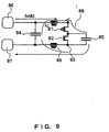
- FIG. 9 illustrates a circuit diagram of a general CMOS integrated circuit.
- FIG. 9 illustrates a PMOS (P-channel MOS) transistor switch 91, a NMOS (N-channel MOS) transistor switch 92, a ground electrode 93, a power supply capacitor 94, a load capacitor 95, a power supply (Vdd) pad 96, a power supply (Vss) pad 97, a charge current 98, and a parasitic inductor 99.
- PMOS P-channel MOS
- NMOS N-channel MOS
- the power supply capacitor 94 has accumulated charge energy.
- the arrangement of the power supply capacitor 94 into the CMOS integrated circuit makes it possible to provide an electric current (Ic) also from the power supply capacitor 94 in addition to the electric current (Ivdd) supplied from the power supply pad 96. Therefore, the variation of current supply from the power supply (Vdd) pad 96 can be controlled.
- di / dt represents a variation of electric current. It is clear from Formula 1 that an effective approach for reduction of power supply noise ( ⁇ V) is either to reduce the variation of electric current (di / dt) or to reduce the parasitic inductor element L. In other words, the parasitic inductor element L increases in proportion to the length of the aluminum wire, so that it is effective to shorten the power supply line on which a current change takes place.
- the present invention provides a LSI layout method for the LSI design by automatic arrangement wiring of standard cells, characterized in that power supply capacitor cells are provided as one of the standard cells in addition to logic gate cells provided as one of the standard cells; the capacitance value of the power supply capacitor cells is determined so as to correspond to the drive load capacity value of the logic gate cells to which the power supply capacitor cells are to be arranged; and the power supply capacitor cells are arranged in the vicinity of the logic gate cells.
- the capacitance value of the power supply capacitor cells is preferably determined to be substantially twice as large as the drive load capacity value of the logic gate cells. If the capacitance value is determined to be about twice as large as the total load capacity of the logic gate standard cells, the power supply noise can be suppressed to about 1/10 or less of the power supply voltage.
- the power supply capacitor cells preferably are arranged in the vicinity of the logic gate cells, which change simultaneously with clock synchronization.
- the present invention provides a LSI layout method for the LSI design using automatic arrangement wiring of standard cells, characterized in that power supply capacitor cells are provided as one of the standard cells, and that the power supply capacitor cells are arranged in spaces of each block where standard cells are not arranged by automatic arrangement wiring.
- the power supply capacitor is arranged in spaces of each circuit block where standard cells are not arranged (dead space).
- the output impedance of power supply can be reduced without increasing the block area, and the power supply noise can be reduced.
- FIG. 1 is a general LSI block diagram
- FIG. 2 is a wiring diagram of Block A formed by automatic arrangement wiring
- FIG. 3 is a wiring diagram formed by automatic arrangement wiring, provided with power supply capacitor cells according to the first embodiment of the LSI layout method of the present invention.
- FIG. 1 illustrates LSI 1 and circuit blocks 11 to 13 in a block layout using standard cells.
- each block is composed of standard cells, and each block is arranged in a rectangular form.
- the present invention is characterized in that standard cells 22 composed of merely power supply capacitors are prepared in advance as standard cells.
- the power supply capacitor standard cells 22 axe arranged in accordance with the load capacity of each logic gate standard cell 21, as illustrated in FIG. 3, in the vicinity of logic gate standard cells 21.
- the term "vicinity" indicates that the power supply capacitor standard cells 22 are placed adjacent to the respective logic gate standard cells 21, which are used for driving load, and that they are arranged on the same power supply lines. Therefore, when the power supply capacitor standard cells are arranged on different power supply lines, regardless of the closeness of both cells, it is not regarded as being placed in the "vicinity".
- the power supply capacitor standard cells 22 are arranged in the vicinity of the logic gate standard cells 21, a charge current toward a load capacity generated when each logic gate standard cell is switching can be provided for the most part from the power supply capacitor placed in the vicinity, so that the power supply noise indicated as the power supply inductor element L in Formula 1 can be reduced.
- the fact that the noise is 1/10 or less of the power supply voltage means that, seen from another perspective, the noise corresponds to about 1/2 of the voltage value of a CMOS threshold voltage.
- the suppression of the power supply noise to 1/2 of the threshold voltage becomes a particularly significant element for securing reliability in LSI operations.
- FIG. 4 As illustrated in FIG. 4 as a cell composition of standard cell type, at the time when an automatic arrangement is executed, drive load capacity of each logic gate (C1+C2) is estimated, and a power supply capacitor standard cell 21 having power supply capacity Cd of at least twice as much as the drive load capacity of each logic gate is placed in the vicinity of each logic gate.
- the power supply capacitor standard cell 21 is placed so as to satisfy Cd > 2 (C1+C2).
- This arrangement assures that the power supply noise ( ⁇ V) can be suppressed to at least 1/10 of the power supply voltage in the respective logic gate circuit.
- the peak value of the power supply noise in the LSI as a whole can be certified.
- FIG. 5 As for the structure of the power supply capacitor, an optimal configuration in a CMOS semiconductor integrated circuit is illustrated in FIG. 5, More specifically, in a p-sub wafer, a n-well is fixed to Vss and a polysilicon gate electrode is fixed to Vdd. The potential of the gate electrode is determined to be forward bias against the n-well, so that depletion layer capacitance is not produced. Therefore, in spite of its small area, a power supply capacitor having a large capacitance value can be realized.
- the arrangement of the power supply capacitor standard cells 22 to all the logic gates creates a large area loss. Furthermore, the power supply noise reaches its peak value when a plurality of logic gates switch simultaneously. Generally, in LSI which operates according to a complete clock-synchronous pattern, a large number of logic gates switch when the clock starts. This is because all the DFF (D Flip-Flop) are designed to operate at the start of the clock. Moreover, with the acceleration of LSI in recent years, the reduction of clock skew is desired.
- DFF D Flip-Flop
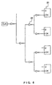
- FIG. 6 illustrates a typical example of a LSI design using the CTS method.
- DFF standard cells 23 and inverter standard cells 24 are illustrated.
- the clock phases of all the DFF standard cells can be adjusted to become the same by changing the size etc. of the inverter according to the load capacity, or by adjusting the number of stage of the inverter delays and so forth.
- power supply capacitor cells are newly prepared in the conventional LSI layout method using standard cells, and the power supply capacitor cells with an optimal capacitance value corresponding to the load capacity of logic gate cells are arranged in the vicinity of the logic gate cells.
- power supply noise caused by parasitic inductors can be prevented from increasing, and the power supply noise element can be reduced.
- the area loss can be kept to a minimum, and the power supply noise can be suppressed efficiently.
- FIG. 7 is a block layout formed by automatic arrangement wiring using conventional standard cells.
- the conventional configuration allows dead spaces 71 to exist, which are empty spaces in blocks where standard cells are not arranged. This is due to the following reason.
- Each block is composed of a plurality of power supply lines on which standard cells are arranged. Since each power supply line is provided with a different number of standard cells, the width of the block in each power supply line differs accordingly, producing these dead spaces.
- the power supply capacitor standard cells 22 are arranged in these dead spaces 71. Accordingly, the power supply capacitor cells can be arranged efficiently without changing the conventional configuration of the block 11 and the total block area.
- the second embodiment makes it possible to add power supply capacitor cells without enlarging the total block area. This embodiment can be realized easily by preparing the power supply capacitor cells 22 as standard cells, calculating the possible number of the power supply capacitor cells 22 to be arranged based on the width of the dead spaces of the power supply and the width of the power supply capacitor cells 22, and arranging as many power supply capacitor cells 22 as possible.
- the power supply capacitor cells 22 are newly prepared, and the power supply capacitor cells 22 are arranged as much as possible in the dead spaces 71, which always existed in each circuit block when automatic arrangement wiring was executed by the conventional method.
- the output impedance of power supply can be reduced without enlarging the total block area, and the power supply noise can be reduced effectively.
- Semiconductor integrated circuits designed with the use of this method have the advantages of generating less power supply noise and preventing malfunction of circuits from occurring and so forth. Therefore, by applying this semiconductor integrated circuit to various systems and devices, systems and devices with improved quality can be provided.
- the LSI layout method of the present invention is applied only to logic gates of dock-synchronous type, so that the area loss can be kept to a minimum, and the power supply noise can be suppressed efficiently.
- power supply capacitor cells are arranged in dead spaces which were already available in each circuit block. This configuration enables the reduction of output impedance of power supply without enlarging the total block area and also the reduction of power supply noise.
Landscapes
- Semiconductor Integrated Circuits (AREA)
- Design And Manufacture Of Integrated Circuits (AREA)
Abstract
A LSI layout method for the LSI design of standard cell type is provided,
by which sufficient noise suppression of power supply noise as well as sufficient
stabilization of power supply can be realized. Power supply capacitor cells are
provided as one of the standard cells in addition to logic gate cells provided as one
of the standard cells. Next, the capacitance value of the power supply capacitor
cells is determined so as to correspond to the drive load capacity value of the logic
gate cells, and the power supply capacitor cells are arranged in the vicinity of the
respective logic gate cells.
Description
This invention relates to a method for stabilizing the power supply in the
LSI design using automatic arrangement wiring of standard cells.
In the last few years, in accordance with the power increasingly consumed
by LSI, LSI tends to generate increased power supply noise. Furthermore, due to
the market demand to promote electric power saving, LSI with lower voltage also
has been developed. With this development, an operating margin against power
supply noise in LSI internal circuits tends to be degraded.
There is a fear that such an increase in power supply noise of LSI may
have negative effects on LSI internal circuits. Examples of such negative effects
are: (1) deterioration of operating speed, (2) malfunction of circuits, and (3) system
malfunction caused by EMI (Electro Magnetic Interference) noise.
For suppression of noise generated from LSI, it has been common to use a
method of arranging a power supply capacity inside LSI. This is because the
insertion of power supply capacity makes it possible to reduce the alternating
current impedance of power supply and to suppress high-frequency noise.
Furthermore, JP5-21711A discloses a method for stabilizing a power
supply, which is achieved by arranging the power supply capacity into sections
where functional circuits of LSI do not exist. In addition, JP5-283615A discloses
a method of efficiently adding power supply capacity by using capacitance between
a power supply and an aluminum wire in LSI.
Generally, in using CMOS (Complementary Metal-Oxide Semiconductor)
integrated circuits, a charge-discharge current is generated toward load capacity
when switching takes place. FIG. 9 illustrates a circuit diagram of a general
CMOS integrated circuit. FIG. 9 illustrates a PMOS (P-channel MOS) transistor
switch 91, a NMOS (N-channel MOS) transistor switch 92, a ground electrode 93,
a power supply capacitor 94, a load capacitor 95, a power supply (Vdd) pad 96, a
power supply (Vss) pad 97, a charge current 98, and a parasitic inductor 99.
With reference to FIG. 9, when the PMOS (P-channel MOS) transistor
switch 91 is turned on, the charge current 98 (Ivdd) flows from the power supply to
the load capacitor 95. When the NMOS (N-channel MOS) transistor switch 92 is
turned on, a discharge current to the ground electrode 93 is generated.
The power supply capacitor 94 has accumulated charge energy. The
arrangement of the power supply capacitor 94 into the CMOS integrated circuit
makes it possible to provide an electric current (Ic) also from the power supply
capacitor 94 in addition to the electric current (Ivdd) supplied from the power
supply pad 96. Therefore, the variation of current supply from the power supply
(Vdd) pad 96 can be controlled.
However, with the increased development of miniature semiconductor
integrated circuits in the last few years, the use of an inductor element (L) of an
aluminum wire inside LSI tends to increase. Moreover, in using a general CMOS
circuit, the parasitic inductor 99 is generated, and this causes power supply noise.
More specifically, the power supply noise (ΔV) can be expressed as:
ΔV=L×di/dt
In the formula 1, di / dt represents a variation of electric current. It is
clear from Formula 1 that an effective approach for reduction of power supply
noise (ΔV) is either to reduce the variation of electric current (di / dt) or to reduce
the parasitic inductor element L. In other words, the parasitic inductor element
L increases in proportion to the length of the aluminum wire, so that it is effective
to shorten the power supply line on which a current change takes place.
However, in the conventional method described above, the aluminum wire
extending from the switched CMOS gate circuit to the power supply capacity was
relatively long, so that the power supply inductor element from the power supply
capacity to the switching circuit was increased largely. Therefore, it was difficult
to achieve sufficient effectiveness for reduction of power supply noise.
In order to solve the above mentioned problems, it is an object of the
present invention to provide a LSI layout method for the LSI design of standard
cell type, by which sufficient noise suppression as well as sufficient stabilization of
the power supply can be achieved.
To achieve this purpose, the present invention provides a LSI layout
method for the LSI design by automatic arrangement wiring of standard cells,
characterized in that power supply capacitor cells are provided as one of the
standard cells in addition to logic gate cells provided as one of the standard cells;
the capacitance value of the power supply capacitor cells is determined so as to
correspond to the drive load capacity value of the logic gate cells to which the
power supply capacitor cells are to be arranged; and the power supply capacitor
cells are arranged in the vicinity of the logic gate cells.
According to this configuration, the power supply capacitor cells are
arranged in the vicinity of the logic gate cells with optimal capacitance values
corresponding to the load capacity of the logic gate cells. Thus, noise caused by
parasitic inductors can be prevented from increasing, and the power supply noise
element can be reduced.
Additionally, in the LSI layout method of the present invention, the
capacitance value of the power supply capacitor cells is preferably determined to
be substantially twice as large as the drive load capacity value of the logic gate
cells. If the capacitance value is determined to be about twice as large as the total
load capacity of the logic gate standard cells, the power supply noise can be
suppressed to about 1/10 or less of the power supply voltage.
Moreover, in the LSI layout method of the present invention, the power
supply capacitor cells preferably are arranged in the vicinity of the logic gate cells,
which change simultaneously with clock synchronization. By arranging the
power supply capacitor cells in the vicinity of the clock-synchronous logic gates, an
area loss can be minimized and the power supply noise can be suppressed
efficiently.
Next, to achieve this purpose, the present invention provides a LSI layout
method for the LSI design using automatic arrangement wiring of standard cells,
characterized in that power supply capacitor cells are provided as one of the
standard cells, and that the power supply capacitor cells are arranged in spaces of
each block where standard cells are not arranged by automatic arrangement
wiring.
According to this configuration, the power supply capacitor is arranged in
spaces of each circuit block where standard cells are not arranged (dead space).
Thus, the output impedance of power supply can be reduced without increasing
the block area, and the power supply noise can be reduced.
Hereinafter, a first embodiment of the LSI layout method of the present
invention will be described with reference to the accompanying drawings. FIG. 1
is a general LSI block diagram; FIG. 2 is a wiring diagram of Block A formed by
automatic arrangement wiring; and FIG. 3 is a wiring diagram formed by
automatic arrangement wiring, provided with power supply capacitor cells
according to the first embodiment of the LSI layout method of the present
invention.
FIG. 1 illustrates LSI 1 and circuit blocks 11 to 13 in a block layout using
standard cells. As illustrated in FIG. 2, each block is composed of standard cells,
and each block is arranged in a rectangular form. The present invention is
characterized in that standard cells 22 composed of merely power supply
capacitors are prepared in advance as standard cells. The power supply capacitor
standard cells 22 axe arranged in accordance with the load capacity of each logic
gate standard cell 21, as illustrated in FIG. 3, in the vicinity of logic gate standard
cells 21.
Here, the term "vicinity" indicates that the power supply capacitor
standard cells 22 are placed adjacent to the respective logic gate standard cells 21,
which are used for driving load, and that they are arranged on the same power
supply lines. Therefore, when the power supply capacitor standard cells are
arranged on different power supply lines, regardless of the closeness of both cells,
it is not regarded as being placed in the "vicinity".
Since the power supply capacitor standard cells 22 are arranged in the
vicinity of the logic gate standard cells 21, a charge current toward a load capacity
generated when each logic gate standard cell is switching can be provided for the
most part from the power supply capacitor placed in the vicinity, so that the power
supply noise indicated as the power supply inductor element L in Formula 1 can
be reduced.
It is generally known that if power supply noise (ΔV) is determined to be
about twice as large as the total load capacity of the logic gate standard cells 21,
ΔV can be suppressed to about 1/10 or less of the power supply voltage (Vdd). (P.
Larsson, "di/dt Noise in CMOS Integrated Circuits.", Analog Integrated Circuits
and Processing, An International Journal Vol. 14, pp.113-129, 1997.)
Furthermore, the fact that the noise is 1/10 or less of the power supply
voltage means that, seen from another perspective, the noise corresponds to about
1/2 of the voltage value of a CMOS threshold voltage. Thus, the suppression of
the power supply noise to 1/2 of the threshold voltage becomes a particularly
significant element for securing reliability in LSI operations.
Specifically, as illustrated in FIG. 4 as a cell composition of standard cell
type, at the time when an automatic arrangement is executed, drive load capacity
of each logic gate (C1+C2) is estimated, and a power supply capacitor standard cell
21 having power supply capacity Cd of at least twice as much as the drive load
capacity of each logic gate is placed in the vicinity of each logic gate. In other
words, the power supply capacitor standard cell 21 is placed so as to satisfy Cd > 2
(C1+C2). This arrangement assures that the power supply noise (ΔV) can be
suppressed to at least 1/10 of the power supply voltage in the respective logic gate
circuit. As a result, the peak value of the power supply noise in the LSI as a
whole can be certified.
As for the structure of the power supply capacitor, an optimal
configuration in a CMOS semiconductor integrated circuit is illustrated in FIG. 5.
More specifically, in a p-sub wafer, a n-well is fixed to Vss and a polysilicon gate
electrode is fixed to Vdd. The potential of the gate electrode is determined to be
forward bias against the n-well, so that depletion layer capacitance is not produced.
Therefore, in spite of its small area, a power supply capacitor having a large
capacitance value can be realized.
On the other hand, the arrangement of the power supply capacitor
standard cells 22 to all the logic gates creates a large area loss. Furthermore, the
power supply noise reaches its peak value when a plurality of logic gates switch
simultaneously. Generally, in LSI which operates according to a complete clock-synchronous
pattern, a large number of logic gates switch when the clock starts.
This is because all the DFF (D Flip-Flop) are designed to operate at the start of the
clock. Moreover, with the acceleration of LSI in recent years, the reduction of
clock skew is desired.
With the foregoing background in mind, a design technique called CTS
(Clock tree Synthesis) is more and more standardized. This method is one of
those methods that can adjust timing so that phases of all the DFF operations
become the same. This timing adjustment can be executed by inverter delays in
view of wiring delays. FIG. 6 illustrates a typical example of a LSI design using
the CTS method. In FIG. 6, DFF standard cells 23 and inverter standard cells 24
are illustrated. The clock phases of all the DFF standard cells can be adjusted to
become the same by changing the size etc. of the inverter according to the load
capacity, or by adjusting the number of stage of the inverter delays and so forth.
As a result of the high precision achieved by the CTS method, all the DFF
now execute switching simultaneously. The problem of power supply noise is
most crucial in such a case. Therefore, in view of the balance to be attained
between the area reduction of LSI as a whole and the noise suppression effects, the
most effective way is to use the above CTS method only for synchronous type logic
gates (DFF gates or inverter gates used for CTS etc.) in arranging the power
supply capacitor standard cells 22.
According to the first embodiment described above, power supply
capacitor cells are newly prepared in the conventional LSI layout method using
standard cells, and the power supply capacitor cells with an optimal capacitance
value corresponding to the load capacity of logic gate cells are arranged in the
vicinity of the logic gate cells. As a result, power supply noise caused by parasitic
inductors can be prevented from increasing, and the power supply noise element
can be reduced. Furthermore, when the above method is applied only to clock-synchronous
type logic gates, the area loss can be kept to a minimum, and the
power supply noise can be suppressed efficiently.
Next, a second embodiment of the LSI layout method of the present
invention will be described with reference to the accompanying drawings. FIG. 7
is a block layout formed by automatic arrangement wiring using conventional
standard cells. As illustrated in FIG. 7, the conventional configuration allows
dead spaces 71 to exist, which are empty spaces in blocks where standard cells are
not arranged. This is due to the following reason. Each block is composed of a
plurality of power supply lines on which standard cells are arranged. Since each
power supply line is provided with a different number of standard cells, the width
of the block in each power supply line differs accordingly, producing these dead
spaces. In the second embodiment, as illustrated in FIG. 8, the power supply
capacitor standard cells 22 are arranged in these dead spaces 71. Accordingly,
the power supply capacitor cells can be arranged efficiently without changing the
conventional configuration of the block 11 and the total block area.
Generally, as the power supply capacitor becomes larger, the output
impedance of the power supply is reduced. Therefore, to suppress power supply
noise effectively, it is advantageous to arrange as many power supply capacitor
cells as possible. On the other hand, the block area is physically limited. The
second embodiment makes it possible to add power supply capacitor cells without
enlarging the total block area. This embodiment can be realized easily by
preparing the power supply capacitor cells 22 as standard cells, calculating the
possible number of the power supply capacitor cells 22 to be arranged based on the
width of the dead spaces of the power supply and the width of the power supply
capacitor cells 22, and arranging as many power supply capacitor cells 22 as
possible.
According to the second embodiment described above, the power supply
capacitor cells 22 are newly prepared, and the power supply capacitor cells 22 are
arranged as much as possible in the dead spaces 71, which always existed in each
circuit block when automatic arrangement wiring was executed by the
conventional method. As a result, the output impedance of power supply can be
reduced without enlarging the total block area, and the power supply noise can be
reduced effectively.
Semiconductor integrated circuits designed with the use of this method
have the advantages of generating less power supply noise and preventing
malfunction of circuits from occurring and so forth. Therefore, by applying this
semiconductor integrated circuit to various systems and devices, systems and
devices with improved quality can be provided.
Moreover, the embodiments described above are only examples of the
present invention and do not limit the present invention thereto. The subject
matter of the present invention is only limited by claims.
According to the LSI layout method of the present invention described
above, in the conventional LSI design using standard cells, power supply capacitor
cells with an optimal capacitance value corresponding to the load capacity of logic
gate cells are arranged in the vicinity of the logic gate cells. Thus, compared with
the conventional LSI layout method, the L-Element of wires in the power supply
can be reduced, so that the power supply noise can be suppressed effectively.
Furthermore, the LSI layout method of the present invention is applied
only to logic gates of dock-synchronous type, so that the area loss can be kept to a
minimum, and the power supply noise can be suppressed efficiently.
In addition, according to the LSI layout method of the present invention,
power supply capacitor cells are arranged in dead spaces which were already
available in each circuit block. This configuration enables the reduction of output
impedance of power supply without enlarging the total block area and also the
reduction of power supply noise.
Claims (4)
- A LSI layout method for a LSI design by automatic arrangement wiring of standard cells, comprising the operations of:providing power supply capacitor cells as one of the standard cells in addition to logic gate cells provided as standard cells,determining a capacitance value of the power supply capacitor cells so as to correspond to a drive load capacity value of the logic gate cells to which the power supply capacitor cells are to be arranged, andarranging the power supply capacitor cells in the vicinity of the logic gate cells.
- The LSI layout method according to claim 1, wherein the capacitance value of the power supply capacitor cells is determined to be substantially twice as large as the drive load capacity value of the logic gate cells.
- The LSI layout method according to claim 1, wherein the power supply capacitor cells are arranged in the vicinity of the logic gate cells which change simultaneously with clock synchronization.
- A LSI layout method for a LSI design by automatic arrangement wiring of standard cells, comprising the operations of:providing power supply capacitor cells as one of the standard cells, andarranging the power supply capacitor cells in spaces of each block where standard cells are not arranged by the automatic arrangement wiring.
Applications Claiming Priority (3)
| Application Number | Priority Date | Filing Date | Title |
|---|---|---|---|
| JP07992799A JP3450739B2 (en) | 1999-03-24 | 1999-03-24 | LSI placement method |
| JP7992799 | 1999-03-24 | ||
| PCT/JP2000/001794 WO2000057470A1 (en) | 1999-03-24 | 2000-03-23 | Method of disposing lsi |
Publications (2)
| Publication Number | Publication Date |
|---|---|
| EP1083598A1 true EP1083598A1 (en) | 2001-03-14 |
| EP1083598A4 EP1083598A4 (en) | 2005-12-21 |
Family
ID=13703955
Family Applications (1)
| Application Number | Title | Priority Date | Filing Date |
|---|---|---|---|
| EP00911324A Withdrawn EP1083598A4 (en) | 1999-03-24 | 2000-03-23 | METHOD FOR ARRANGING A LSI CIRCUIT |
Country Status (5)
| Country | Link |
|---|---|
| EP (1) | EP1083598A4 (en) |
| JP (1) | JP3450739B2 (en) |
| KR (1) | KR100389235B1 (en) |
| CN (1) | CN1149657C (en) |
| WO (1) | WO2000057470A1 (en) |
Cited By (1)
| Publication number | Priority date | Publication date | Assignee | Title |
|---|---|---|---|---|
| US7334210B2 (en) | 2003-11-04 | 2008-02-19 | Matsushita Electric Industrial Co., Ltd. | Semiconductor integrated circuit and method of designing the same |
Families Citing this family (10)
| Publication number | Priority date | Publication date | Assignee | Title |
|---|---|---|---|---|
| US6732335B2 (en) | 2002-04-23 | 2004-05-04 | Oki Electric Industry Co., Ltd. | Semiconductor IC with an inside capacitor for a power supply circuit and a method of automatically designing the same |
| JP2004055954A (en) * | 2002-07-23 | 2004-02-19 | Nec Micro Systems Ltd | Semiconductor integrated circuit and layout method thereof |
| CN1294642C (en) * | 2002-08-21 | 2007-01-10 | 矽统科技股份有限公司 | Analysis method and reduction method of power supply noise |
| JP4205662B2 (en) | 2004-12-28 | 2009-01-07 | パナソニック株式会社 | Semiconductor integrated circuit design method |
| JP5092263B2 (en) * | 2006-03-31 | 2012-12-05 | 富士通セミコンダクター株式会社 | Decoupling capacitor and semiconductor integrated circuit device |
| JP4967534B2 (en) * | 2006-08-28 | 2012-07-04 | 富士通セミコンダクター株式会社 | Semiconductor device layout method and layout program |
| JP5653001B2 (en) | 2009-03-16 | 2015-01-14 | ピーエスフォー ルクスコ エスエイアールエルPS4 Luxco S.a.r.l. | Semiconductor device and method of arranging compensation capacitance of semiconductor device |
| JP5552775B2 (en) * | 2009-08-28 | 2014-07-16 | ソニー株式会社 | Semiconductor integrated circuit |
| JP5640712B2 (en) * | 2010-12-10 | 2014-12-17 | 日本電気株式会社 | Semiconductor device design support device, capacitor placement method, and program |
| CN116805144A (en) * | 2022-03-18 | 2023-09-26 | 圣邦微电子(北京)股份有限公司 | DAC layout wiring method and system |
Family Cites Families (6)
| Publication number | Priority date | Publication date | Assignee | Title |
|---|---|---|---|---|
| JP2682397B2 (en) * | 1993-10-07 | 1997-11-26 | 日本電気株式会社 | Cell-based design semiconductor integrated circuit device |
| US5631492A (en) * | 1994-01-21 | 1997-05-20 | Motorola | Standard cell having a capacitor and a power supply capacitor for reducing noise and method of formation |
| JP3584693B2 (en) * | 1996-09-18 | 2004-11-04 | 株式会社デンソー | Semiconductor integrated circuit |
| JPH10107235A (en) * | 1996-09-27 | 1998-04-24 | Hitachi Ltd | Gate array LSI configuration method and circuit device using the same |
| JPH10284605A (en) * | 1997-04-08 | 1998-10-23 | Mitsubishi Electric Corp | Semiconductor integrated circuit and semiconductor integrated circuit layout-designed by cell-based method |
| JP2947222B2 (en) * | 1997-05-23 | 1999-09-13 | 日本電気株式会社 | Semiconductor integrated circuit |
-
1999
- 1999-03-24 JP JP07992799A patent/JP3450739B2/en not_active Expired - Fee Related
-
2000
- 2000-03-23 CN CNB008009791A patent/CN1149657C/en not_active Expired - Fee Related
- 2000-03-23 KR KR10-2000-7013241A patent/KR100389235B1/en not_active Expired - Fee Related
- 2000-03-23 WO PCT/JP2000/001794 patent/WO2000057470A1/en not_active Ceased
- 2000-03-23 EP EP00911324A patent/EP1083598A4/en not_active Withdrawn
Cited By (1)
| Publication number | Priority date | Publication date | Assignee | Title |
|---|---|---|---|---|
| US7334210B2 (en) | 2003-11-04 | 2008-02-19 | Matsushita Electric Industrial Co., Ltd. | Semiconductor integrated circuit and method of designing the same |
Also Published As
| Publication number | Publication date |
|---|---|
| KR100389235B1 (en) | 2003-06-27 |
| JP3450739B2 (en) | 2003-09-29 |
| CN1310862A (en) | 2001-08-29 |
| JP2000277618A (en) | 2000-10-06 |
| EP1083598A4 (en) | 2005-12-21 |
| KR20010043810A (en) | 2001-05-25 |
| CN1149657C (en) | 2004-05-12 |
| WO2000057470A1 (en) | 2000-09-28 |
Similar Documents
| Publication | Publication Date | Title |
|---|---|---|
| TWI826746B (en) | Semiconductor layout in finfet technologies | |
| US7514766B2 (en) | Semiconductor device | |
| EP1083598A1 (en) | Method of disposing lsi | |
| EP0319063A2 (en) | Voltage multiplier circuit and rectifier element | |
| US6384675B1 (en) | Differencing non-overlapped dual-output amplifier circuit | |
| CN107888179B (en) | Semiconductor device | |
| JP4420156B2 (en) | Semiconductor device | |
| JP2022125281A (en) | Semiconductor device | |
| US5905291A (en) | MISFET semiconductor integrated circuit device | |
| JP5763670B2 (en) | Semiconductor integrated circuit | |
| US7602231B2 (en) | Charge-pump circuit | |
| US6608365B1 (en) | Low leakage PMOS on-chip decoupling capacitor cells compatible with standard CMOS cells | |
| US20030214347A1 (en) | Basic stage for a charge pump circuit | |
| JP3035188B2 (en) | Semiconductor device | |
| US6934171B2 (en) | Semiconductor integrated circuit having voltage-down circuit regulator and charge sharing | |
| JPH10135336A (en) | Semiconductor integrated circuit device, method of reducing noise generated by semiconductor integrated circuit device, and internal power supply system of semiconductor integrated circuit device | |
| US5930191A (en) | Semiconductor memory device having a plurality of power voltages | |
| JP3411025B2 (en) | Semiconductor integrated circuit device | |
| JP3498641B2 (en) | Low power consumption type semiconductor integrated circuit device | |
| JP2005005757A (en) | Synchronizing circuit and semiconductor chip employing same | |
| JP2002110798A (en) | Semiconductor device and layout method thereof | |
| Hasan et al. | On-chip high voltage charge pump in standard low voltage CMOS process | |
| KR20060001305A (en) | Pumping Capacitors Used in Pumping Circuits | |
| US20130027016A1 (en) | Standard cell circuit, semiconductor integrated circuit, and semiconductor integrated circuit device | |
| GB2348556A (en) | A CMOS gate array with internal MOS supply decoupling capacitors |
Legal Events
| Date | Code | Title | Description |
|---|---|---|---|
| PUAI | Public reference made under article 153(3) epc to a published international application that has entered the european phase |
Free format text: ORIGINAL CODE: 0009012 |
|
| 17P | Request for examination filed |
Effective date: 20001211 |
|
| AK | Designated contracting states |
Kind code of ref document: A1 Designated state(s): AT BE CH CY DE DK ES FI FR GB GR IE IT LI LU MC NL PT SE |
|
| RBV | Designated contracting states (corrected) |
Designated state(s): DE FR GB NL |
|
| A4 | Supplementary search report drawn up and despatched |
Effective date: 20051107 |
|
| STAA | Information on the status of an ep patent application or granted ep patent |
Free format text: STATUS: THE APPLICATION HAS BEEN WITHDRAWN |
|
| 18W | Application withdrawn |
Effective date: 20080715 |