EP1080924A1 - Thermal head - Google Patents
Thermal head Download PDFInfo
- Publication number
- EP1080924A1 EP1080924A1 EP00306384A EP00306384A EP1080924A1 EP 1080924 A1 EP1080924 A1 EP 1080924A1 EP 00306384 A EP00306384 A EP 00306384A EP 00306384 A EP00306384 A EP 00306384A EP 1080924 A1 EP1080924 A1 EP 1080924A1
- Authority
- EP
- European Patent Office
- Prior art keywords
- thermal head
- heater resistors
- insulating substrate
- individual electrodes
- electrically connected
- Prior art date
- Legal status (The legal status is an assumption and is not a legal conclusion. Google has not performed a legal analysis and makes no representation as to the accuracy of the status listed.)
- Granted
Links
Images


Classifications
-
- H—ELECTRICITY
- H04—ELECTRIC COMMUNICATION TECHNIQUE
- H04N—PICTORIAL COMMUNICATION, e.g. TELEVISION
- H04N1/00—Scanning, transmission or reproduction of documents or the like, e.g. facsimile transmission; Details thereof
- H04N1/024—Details of scanning heads ; Means for illuminating the original
- H04N1/028—Details of scanning heads ; Means for illuminating the original for picture information pick-up
-
- B—PERFORMING OPERATIONS; TRANSPORTING
- B41—PRINTING; LINING MACHINES; TYPEWRITERS; STAMPS
- B41J—TYPEWRITERS; SELECTIVE PRINTING MECHANISMS, i.e. MECHANISMS PRINTING OTHERWISE THAN FROM A FORME; CORRECTION OF TYPOGRAPHICAL ERRORS
- B41J2/00—Typewriters or selective printing mechanisms characterised by the printing or marking process for which they are designed
- B41J2/315—Typewriters or selective printing mechanisms characterised by the printing or marking process for which they are designed characterised by selective application of heat to a heat sensitive printing or impression-transfer material
- B41J2/32—Typewriters or selective printing mechanisms characterised by the printing or marking process for which they are designed characterised by selective application of heat to a heat sensitive printing or impression-transfer material using thermal heads
- B41J2/335—Structure of thermal heads
- B41J2/33505—Constructional details
- B41J2/3351—Electrode layers
-
- B—PERFORMING OPERATIONS; TRANSPORTING
- B41—PRINTING; LINING MACHINES; TYPEWRITERS; STAMPS
- B41J—TYPEWRITERS; SELECTIVE PRINTING MECHANISMS, i.e. MECHANISMS PRINTING OTHERWISE THAN FROM A FORME; CORRECTION OF TYPOGRAPHICAL ERRORS
- B41J2/00—Typewriters or selective printing mechanisms characterised by the printing or marking process for which they are designed
- B41J2/315—Typewriters or selective printing mechanisms characterised by the printing or marking process for which they are designed characterised by selective application of heat to a heat sensitive printing or impression-transfer material
- B41J2/32—Typewriters or selective printing mechanisms characterised by the printing or marking process for which they are designed characterised by selective application of heat to a heat sensitive printing or impression-transfer material using thermal heads
- B41J2/335—Structure of thermal heads
- B41J2/33505—Constructional details
- B41J2/3352—Integrated circuits
-
- B—PERFORMING OPERATIONS; TRANSPORTING
- B41—PRINTING; LINING MACHINES; TYPEWRITERS; STAMPS
- B41J—TYPEWRITERS; SELECTIVE PRINTING MECHANISMS, i.e. MECHANISMS PRINTING OTHERWISE THAN FROM A FORME; CORRECTION OF TYPOGRAPHICAL ERRORS
- B41J2/00—Typewriters or selective printing mechanisms characterised by the printing or marking process for which they are designed
- B41J2/315—Typewriters or selective printing mechanisms characterised by the printing or marking process for which they are designed characterised by selective application of heat to a heat sensitive printing or impression-transfer material
- B41J2/32—Typewriters or selective printing mechanisms characterised by the printing or marking process for which they are designed characterised by selective application of heat to a heat sensitive printing or impression-transfer material using thermal heads
- B41J2/335—Structure of thermal heads
- B41J2/33555—Structure of thermal heads characterised by type
- B41J2/3356—Corner type resistors
-
- B—PERFORMING OPERATIONS; TRANSPORTING
- B41—PRINTING; LINING MACHINES; TYPEWRITERS; STAMPS
- B41J—TYPEWRITERS; SELECTIVE PRINTING MECHANISMS, i.e. MECHANISMS PRINTING OTHERWISE THAN FROM A FORME; CORRECTION OF TYPOGRAPHICAL ERRORS
- B41J2/00—Typewriters or selective printing mechanisms characterised by the printing or marking process for which they are designed
- B41J2/315—Typewriters or selective printing mechanisms characterised by the printing or marking process for which they are designed characterised by selective application of heat to a heat sensitive printing or impression-transfer material
- B41J2/32—Typewriters or selective printing mechanisms characterised by the printing or marking process for which they are designed characterised by selective application of heat to a heat sensitive printing or impression-transfer material using thermal heads
- B41J2/335—Structure of thermal heads
- B41J2/33555—Structure of thermal heads characterised by type
- B41J2/3357—Surface type resistors
-
- B—PERFORMING OPERATIONS; TRANSPORTING
- B41—PRINTING; LINING MACHINES; TYPEWRITERS; STAMPS
- B41J—TYPEWRITERS; SELECTIVE PRINTING MECHANISMS, i.e. MECHANISMS PRINTING OTHERWISE THAN FROM A FORME; CORRECTION OF TYPOGRAPHICAL ERRORS
- B41J2/00—Typewriters or selective printing mechanisms characterised by the printing or marking process for which they are designed
- B41J2/315—Typewriters or selective printing mechanisms characterised by the printing or marking process for which they are designed characterised by selective application of heat to a heat sensitive printing or impression-transfer material
- B41J2/32—Typewriters or selective printing mechanisms characterised by the printing or marking process for which they are designed characterised by selective application of heat to a heat sensitive printing or impression-transfer material using thermal heads
- B41J2/335—Structure of thermal heads
- B41J2/33595—Conductors through the layered structure
-
- B—PERFORMING OPERATIONS; TRANSPORTING
- B41—PRINTING; LINING MACHINES; TYPEWRITERS; STAMPS
- B41J—TYPEWRITERS; SELECTIVE PRINTING MECHANISMS, i.e. MECHANISMS PRINTING OTHERWISE THAN FROM A FORME; CORRECTION OF TYPOGRAPHICAL ERRORS
- B41J2/00—Typewriters or selective printing mechanisms characterised by the printing or marking process for which they are designed
- B41J2/315—Typewriters or selective printing mechanisms characterised by the printing or marking process for which they are designed characterised by selective application of heat to a heat sensitive printing or impression-transfer material
- B41J2/32—Typewriters or selective printing mechanisms characterised by the printing or marking process for which they are designed characterised by selective application of heat to a heat sensitive printing or impression-transfer material using thermal heads
- B41J2/345—Typewriters or selective printing mechanisms characterised by the printing or marking process for which they are designed characterised by selective application of heat to a heat sensitive printing or impression-transfer material using thermal heads characterised by the arrangement of resistors or conductors
Definitions
- the present invention relates to a thermal head for use in thermal recording in a facsimile machine, a printer, or the like.
- an individual electrode 3 connected to one end of a heater resistor 2 is connected to a driving element 5.
- the other end of the heater resistor 2 is connected to a common electrode 4. All of them are provided on the same plane on an insulating substrate 1.
- the individual electrode 3 and the driving element 5 are connected by wire bonding or flip chip.
- the driving element 5 and the connecting portion are, for protection, encapsulated on the periphery of the driving element using epoxy resin or the like.
- the encapsulation covers the whole of the driving element 5 and the connecting portion, and further, for the purpose of securing the reliability, has the width and the height which are larger than those of the driving element 5 and the connecting portion. This follows that, in order to avoid interference with a platen for advancing paper by rotating together with the paper, the position of the encapsulation is required to be apart from the heater resistor 2 by a predetermined distance.
- the thermal head in order to lower the cost of the thermal head, it is necessary to make the width of the substrate as small as possible to increase the number of the thermal heads taken from one process unit substrate. Therefore, by, for example, making the platen diameter as small as possible to avoid the interference and to realize both decrease in the width of the substrate and the avoidance of the interference between the encapsulation and the paper 9 and the platen 8.
- the platen diameter has problems such as insufficient strength and deflection of the platen and decrease in the amount of collapse (contact area with the paper) by pressing pressure, and thus, adversely affects the printing quality. Therefore, about 5 mm to 10 mm is thought to be the lower limit of the platen diameter, which means that, in order to avoid the interference with the encapsulation, it is not possible to make the width of the substrate smaller beyond a certain extent.
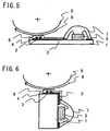
- an end face type thermal head as shown in Fig. 6 where the heater resistor 2 is provided on an end face of the substrate and the driving element 5 is provided perpendicularly to the heater resistor 2 and a near edge type thermal head as shown in Fig. 7 where the interference with the encapsulated portion is avoided by providing the heater resistor 2 at an edge portion of the substrate and slanting the thermal head are used.
- a concave portion is processed in a part of the insulating substrate 1 such that a step is provided in the substrate itself for making a portion where the driving element 5 is provided lower than the heater resistor 2.
- a driving element can be provided on the rear surface of a heater resistor.
- the substrate size can be made smaller.
- the platen diameter has to be made smaller to make the thermal head size smaller, a necessary platen diameter can be selected independently of the width of the substrate.
- the driving element on the rear surface, area for the provision of the driving element which is conventionally necessary becomes unnecessary, and the width of the substrate can be made further smaller.
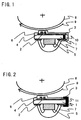
- Fig. 1 is a cross-sectional view of an embodiment using through hole connection.
- the thermal head is of a U-turn electrode constitution where two heater resistors form one dot.
- pairs of two heater resistors 2 with each pair forming one dot are arranged in a line on the front surface side of an insulating substrate 1.
- One heater resistor of each pair is electrically connected to an individual electrode 3 and the other heater resistor is electrically connected to a common electrode 4 with a U-turn electrode sandwiched between the heater resistors.
- the periphery is protected by a protective film.
- the end of each of the individual electrodes which is opposite to the end connected to a heater resistor is connected to a through hole. Electric connection to the rear surface side of the insulating substrate 1 is carried out through the through hole 10.
- the individual electrode is further extended through each of the through holes.
- Each of the individual electrodes is connected to a driving element 5 by wire bonding, flip chip, or the like.
- the driving element and the connecting portion are covered with encapsulation 7 formed of a resin of an epoxy system or the like.
- all the common electrodes are connected together in a strip-like pattern on one side of the insulating substrate 1. Electric connection to the rear surface side of the insulating substrate 1 is carried out through a plurality of through holes in the pattern. By electric current passing from the common electrodes to the individual electrodes selected by the driving element, a part of the heater resistors generate heat.
- the diameter of the through holes is 0.05 mm or smaller and the intervals between the through holes are 0.1 mm or smaller. This is because the dot pitch in case the dot density of the heater resistors is 200 DPI (8 dots/mm) is 0.125 mm.
- the diameter is 0.05 mm or larger and the intervals between the through holes are 0.1 mm or larger. In that case, it is necessary to effectively arrange the through holes so as to be staggered according to their size. This is also true of the case of 200 DPI or more.
- Fig. 2 is a cross-sectional view of an embodiment,using turnup terminal connection.
- the thermal head is of a common electrode constitution where one heater resistor forms one dot.
- heater resistors 2 each forming one dot are arranged in a line on the front surface side of an insulating substrate 1.
- One end of each heater resistor is electrically connected to an individual electrode 3 and the other end is electrically connected to a common electrode 4.
- the periphery is protected by a protective film.
- One end of each of the individual electrodes is connected to a heater resistor.
- the other end extends to the vicinity of an end face of the insulating substrate, and is electrically connected to the rear surface side of the insulating substrate 1 using a turnup connection terminal 11.
- the respective turnup connection terminals are connected so as to make one-to-one correspondence to individual electrodes on the rear surface side.
- Each of the individual electrodes is connected to a driving element 5 by wire bonding, flip chip, or the like.
- the driving element and the connecting portion are covered with encapsulation 7 formed of a resin of an epoxy system or the like.
- the terminal pitch of the turnup connection terminals is 0.1 mm or smaller and the space between terminal widths is sufficient. This is because the dot pitch in case the density of the heater resistors is 200 DPI (8 dots/mm) is 0.125 mm, and for the purpose of avoiding short circuit between adjacent dots due to misalignment when the terminals are connected or misalignment in patterning between the front and rear surfaces. In case of 200 DPI or more, turnup connection terminals having a narrower pitch according to the size are necessary.
- a method where a flexible pattern circuit (FPC) is used and the connection is carried out by soldering or an anisotropic conductive film, a method where clip-like metal terminals are aligned, a method where the connection is carried out by wire bonding, or the like is used. It is necessary that the current capacitance of 5 - 100 mA or more can be secured per terminal.
- FPC flexible pattern circuit
- a thermal head according to the present invention there is no encapsulation on the side where the heaters are provided, and a straight path which is completely flat can be materialized.
- the driving elements By providing the driving elements on the rear surface, area for the provision of the driving elements which is conventionally necessary becomes unnecessary on the side where the heater resistors are provided, and the width of the substrate can be made further smaller.
- the platen diameter has to be made smaller at the expense of the printing quality, in this invention a necessary platen diameter can be selected independently of the width of the substrate, and the degree of freedom in designing the thermal printer is remarkably improved.
- the shape in going through the manufacturing process is simplified, the number of the thermal heads taken from one process unit substrate is increased, and the productivity is improved, which greatly contributes to lowering of the cost.
Landscapes
- Engineering & Computer Science (AREA)
- Microelectronics & Electronic Packaging (AREA)
- Multimedia (AREA)
- Signal Processing (AREA)
- Electronic Switches (AREA)
Abstract
Description
- The present invention relates to a thermal head for use in thermal recording in a facsimile machine, a printer, or the like.
- In a conventional thermal head, as shown in Fig. 5, an
individual electrode 3 connected to one end of aheater resistor 2 is connected to adriving element 5. The other end of theheater resistor 2 is connected to acommon electrode 4. All of them are provided on the same plane on aninsulating substrate 1. - The
individual electrode 3 and thedriving element 5 are connected by wire bonding or flip chip. Thedriving element 5 and the connecting portion are, for protection, encapsulated on the periphery of the driving element using epoxy resin or the like. The encapsulation covers the whole of thedriving element 5 and the connecting portion, and further, for the purpose of securing the reliability, has the width and the height which are larger than those of thedriving element 5 and the connecting portion. This follows that, in order to avoid interference with a platen for advancing paper by rotating together with the paper, the position of the encapsulation is required to be apart from theheater resistor 2 by a predetermined distance. However, on the other hand, in order to lower the cost of the thermal head, it is necessary to make the width of the substrate as small as possible to increase the number of the thermal heads taken from one process unit substrate. Therefore, by, for example, making the platen diameter as small as possible to avoid the interference and to realize both decrease in the width of the substrate and the avoidance of the interference between the encapsulation and thepaper 9 and theplaten 8. However, to make small the platen diameter has problems such as insufficient strength and deflection of the platen and decrease in the amount of collapse (contact area with the paper) by pressing pressure, and thus, adversely affects the printing quality. Therefore, about 5 mm to 10 mm is thought to be the lower limit of the platen diameter, which means that, in order to avoid the interference with the encapsulation, it is not possible to make the width of the substrate smaller beyond a certain extent. - Since, in this constitution, paper is inserted so as to keep out of the encapsulated portion, the paper insert path is curved, and thus, hard cardboard, plastic paper which is difficult to fold, and the like can not be used for printing. Therefore, conventionally, with regard to these kinds of paper difficult to fold, in order to secure a straight path (a straight paper insert path), an end face type thermal head as shown in Fig. 6 where the
heater resistor 2 is provided on an end face of the substrate and thedriving element 5 is provided perpendicularly to theheater resistor 2 and a near edge type thermal head as shown in Fig. 7 where the interference with the encapsulated portion is avoided by providing theheater resistor 2 at an edge portion of the substrate and slanting the thermal head are used. Further, recently, a method has been thought of where, as shown in Fig. 8, a concave portion is processed in a part of theinsulating substrate 1 such that a step is provided in the substrate itself for making a portion where thedriving element 5 is provided lower than theheater resistor 2. - However, with regard to all of the above-described methods, since the shape of the substrate is complicated, its processing is difficult, and, since its patterning has to be carried out with regard to different surfaces or a surface having a great step, the manufacturing method is complicated and it is difficult to lower the cost.
- In order to solve these problems, according to the present invention, by carrying out electric connection between front and rear surfaces of a substrate using through hole connection or turnup terminal connection, a driving element can be provided on the rear surface of a heater resistor.
- By the present invention, there is no encapsulation on the side where the heater is provided, a straight path which is completely flat can be materialized, and there is no interference between a platen and paper and encapsulation. Therefore, the substrate size can be made smaller. Further, though, conventionally, the platen diameter has to be made smaller to make the thermal head size smaller, a necessary platen diameter can be selected independently of the width of the substrate. Still further, by providing the driving element on the rear surface, area for the provision of the driving element which is conventionally necessary becomes unnecessary, and the width of the substrate can be made further smaller.
- Embodiments of the present invention will now be described by way of example only and with reference to the accompanying drawings, in which:-
- Fig. 1 is a cross-sectional view of a thermal head in case through hole connection is used according to the present invention;
- Fig. 2 is a cross-sectional view of a thermal head in case turnup terminal connection is used according to the present invention;
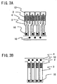
- Fig. 3 is a plan view of the thermal head in case the through hole connection is used according to the present invention;
- Fig. 4 is a plan view of the thermal head in case the turnup terminal connection is used according to the present invention;
- Fig. 5 is a cross-sectional view showing a conventional thermal head;
- Fig. 6 is across-sectional view showing another conventional thermal head;
- Fig. 7 is a cross-sectional view showing still another conventional thermal head; and
- Fig. 8 is a cross-sectional view showing yet still another conventional thermal head.
-
- An embodiment of the present invention is described in the following in detail based on the drawings.
- Fig. 1 is a cross-sectional view of an embodiment using through hole connection. As shown in Fig. 3A, the thermal head is of a U-turn electrode constitution where two heater resistors form one dot.
- In Fig. 1, pairs of two
heater resistors 2 with each pair forming one dot are arranged in a line on the front surface side of aninsulating substrate 1. One heater resistor of each pair is electrically connected to anindividual electrode 3 and the other heater resistor is electrically connected to acommon electrode 4 with a U-turn electrode sandwiched between the heater resistors. The periphery is protected by a protective film. The end of each of the individual electrodes which is opposite to the end connected to a heater resistor is connected to a through hole. Electric connection to the rear surface side of theinsulating substrate 1 is carried out through the throughhole 10. On the rear surface side, the individual electrode is further extended through each of the through holes. Each of the individual electrodes is connected to adriving element 5 by wire bonding, flip chip, or the like. The driving element and the connecting portion are covered withencapsulation 7 formed of a resin of an epoxy system or the like. - On the other hand, with regard to the side of the common electrodes, all the common electrodes are connected together in a strip-like pattern on one side of the
insulating substrate 1. Electric connection to the rear surface side of theinsulating substrate 1 is carried out through a plurality of through holes in the pattern. By electric current passing from the common electrodes to the individual electrodes selected by the driving element, a part of the heater resistors generate heat. - Here, preferably, the diameter of the through holes is 0.05 mm or smaller and the intervals between the through holes are 0.1 mm or smaller. This is because the dot pitch in case the dot density of the heater resistors is 200 DPI (8 dots/mm) is 0.125 mm. However, in actual formation of the through holes, if it is difficult to process such through holes having a small diameter at such a small pitch, it does not matter even if the diameter is 0.05 mm or larger and the intervals between the through holes are 0.1 mm or larger. In that case, it is necessary to effectively arrange the through holes so as to be staggered according to their size. This is also true of the case of 200 DPI or more.
- In order to carry out electric connection between the front and rear surfaces of the insulating substrate through the through holes, a method where the inside of the through holes is filled with a conductor, a method using wet plating, a method using vacuum film formation, or the like is used. It is necessary that the current capacitance of 5 - 100 mA or more can be secured per through hole.
- The above description is with regard to the case of the thermal head having the U-turn electrode constitution. However, the same can be said with regard to a thermal head having a common electrode constitution where one dot is formed of one heater resistor as shown in Fig. 3B.
- Fig. 2 is a cross-sectional view of an embodiment,using turnup terminal connection. As shown in Fig. 4A, the thermal head is of a common electrode constitution where one heater resistor forms one dot.
- In Fig. 2,
heater resistors 2 each forming one dot are arranged in a line on the front surface side of aninsulating substrate 1. One end of each heater resistor is electrically connected to anindividual electrode 3 and the other end is electrically connected to acommon electrode 4. The periphery is protected by a protective film. One end of each of the individual electrodes is connected to a heater resistor. The other end extends to the vicinity of an end face of the insulating substrate, and is electrically connected to the rear surface side of theinsulating substrate 1 using aturnup connection terminal 11. On the rear surface side, the respective turnup connection terminals are connected so as to make one-to-one correspondence to individual electrodes on the rear surface side. Each of the individual electrodes is connected to adriving element 5 by wire bonding, flip chip, or the like. The driving element and the connecting portion are covered withencapsulation 7 formed of a resin of an epoxy system or the like. - On the other hand, with regard to the side of the common electrodes, all the common electrodes are connected together in a strip-like pattern on one side of the insulating
substrate 1. Electric connection to the rear surface side of the insulatingsubstrate 1 is carried out through the turnup connection terminals in the pattern. By electric current passing from the common electrodes to the individual electrodes selected by the driving element, a part of the heater resistors generate heat. - Here, preferably, the terminal pitch of the turnup connection terminals is 0.1 mm or smaller and the space between terminal widths is sufficient. This is because the dot pitch in case the density of the heater resistors is 200 DPI (8 dots/mm) is 0.125 mm, and for the purpose of avoiding short circuit between adjacent dots due to misalignment when the terminals are connected or misalignment in patterning between the front and rear surfaces. In case of 200 DPI or more, turnup connection terminals having a narrower pitch according to the size are necessary.
- In order to carry out electric connection between the front and rear surfaces of the insulating substrate through the turnup connection terminals, a method where a flexible pattern circuit (FPC) is used and the connection is carried out by soldering or an anisotropic conductive film, a method where clip-like metal terminals are aligned, a method where the connection is carried out by wire bonding, or the like is used. It is necessary that the current capacitance of 5 - 100 mA or more can be secured per terminal.
- The above description is with regard to the case of the thermal head having the common electrode constitution where the strip-like common electrode is provided in the vicinity of the heaters. However, the same can be said with regard to a thermal head of a type where common electrodes are wired on both sides of an insulating substrate as shown in Fig. 4B.
- By a thermal head according to the present invention, there is no encapsulation on the side where the heaters are provided, and a straight path which is completely flat can be materialized. By providing the driving elements on the rear surface, area for the provision of the driving elements which is conventionally necessary becomes unnecessary on the side where the heater resistors are provided, and the width of the substrate can be made further smaller. Still further, though conventionally, for the purpose of making the thermal head size smaller, the platen diameter has to be made smaller at the expense of the printing quality, in this invention a necessary platen diameter can be selected independently of the width of the substrate, and the degree of freedom in designing the thermal printer is remarkably improved.
- Also, the shape in going through the manufacturing process is simplified, the number of the thermal heads taken from one process unit substrate is increased, and the productivity is improved, which greatly contributes to lowering of the cost.
Claims (3)
- A thermal head comprising heater resistors arranged in a line on an insulating substrate, individual electrodes electrically connected to said heater resistors, respectively, common electrodes disposed so as to be electrically connected to said individual electrodes through said heater resistors, a protective film for protecting said heater resistors, said individual electrodes, and said common electrodes, and driving elements connected to said individual electrodes, respectively, part of said heater resistors generating heat by electric current from said common electrodes passing through said individual electrodes selected by said driving elements, wherein: said individual electrodes electrically connected to said heater resistors and said common electrode are electrically connected between front and rear surfaces of said insulating substrate, and said driving elements are provided on the opposite surface to the surface where said heater resistors are provided.
- A thermal head as claimed in claim 1, wherein said electric connection between said front and rear surfaces is carried out through through holes penetrating in the thickness direction of said insulating substrate.
- A thermal head as claimed in claim 1, wherein said electric connection between said front and rear surfaces is carried out through turnup connection terminals on an end face of said insulating substrate.
Applications Claiming Priority (2)
| Application Number | Priority Date | Filing Date | Title |
|---|---|---|---|
| JP21835299 | 1999-08-02 | ||
| JP11218352A JP2001038941A (en) | 1999-08-02 | 1999-08-02 | Thermal head |
Publications (2)
| Publication Number | Publication Date |
|---|---|
| EP1080924A1 true EP1080924A1 (en) | 2001-03-07 |
| EP1080924B1 EP1080924B1 (en) | 2003-09-17 |
Family
ID=16718545
Family Applications (1)
| Application Number | Title | Priority Date | Filing Date |
|---|---|---|---|
| EP00306384A Expired - Lifetime EP1080924B1 (en) | 1999-08-02 | 2000-07-27 | Thermal head |
Country Status (6)
| Country | Link |
|---|---|
| US (1) | US6271873B1 (en) |
| EP (1) | EP1080924B1 (en) |
| JP (1) | JP2001038941A (en) |
| KR (1) | KR100662531B1 (en) |
| CN (1) | CN1168606C (en) |
| DE (1) | DE60005269T2 (en) |
Cited By (2)
| Publication number | Priority date | Publication date | Assignee | Title |
|---|---|---|---|---|
| EP1419888A3 (en) * | 2002-11-13 | 2004-07-28 | Agfa-Gevaert | Thermal head printer and process for printing substantially light-insensitive recording materials. |
| US7023460B2 (en) | 2002-11-13 | 2006-04-04 | Agfa Gevaert | Thermal head printer and process for printing substantially light-insensitive recording material |
Families Citing this family (9)
| Publication number | Priority date | Publication date | Assignee | Title |
|---|---|---|---|---|
| JP2004006299A (en) * | 2002-04-22 | 2004-01-08 | Canon Inc | Heater having heating resistor on substrate and image heating apparatus using this heater |
| JP4354339B2 (en) * | 2004-06-08 | 2009-10-28 | アルプス電気株式会社 | Thermal head |
| JP5063018B2 (en) * | 2005-07-28 | 2012-10-31 | 京セラ株式会社 | Recording head and printer using the same |
| JP5049894B2 (en) * | 2008-06-24 | 2012-10-17 | アルプス電気株式会社 | Thermal head |
| JP2011126025A (en) * | 2009-12-15 | 2011-06-30 | Seiko Instruments Inc | Thermal head and printer |
| JP5964101B2 (en) * | 2012-03-27 | 2016-08-03 | 東芝ホクト電子株式会社 | Thermal print head |
| JP6209019B2 (en) * | 2013-08-20 | 2017-10-04 | ローム株式会社 | Thermal print head, thermal printer |
| JP7630494B2 (en) * | 2020-04-01 | 2025-02-17 | ローム株式会社 | Thermal printhead and method for manufacturing the same |
| CN112721460B (en) * | 2021-01-13 | 2023-11-17 | 广州晖印科技有限公司 | Thermal print head with separated reverse structure |
Citations (7)
| Publication number | Priority date | Publication date | Assignee | Title |
|---|---|---|---|---|
| JPS6225067A (en) * | 1985-07-25 | 1987-02-03 | Ricoh Co Ltd | Method of forming thermal head electrodes |
| JPS6399964A (en) * | 1986-10-17 | 1988-05-02 | Matsushita Electric Ind Co Ltd | thermal head |
| JPH02128863A (en) * | 1988-11-09 | 1990-05-17 | Graphtec Corp | Thermal head array |
| JPH0383659A (en) * | 1989-08-28 | 1991-04-09 | Sharp Corp | Thermal head |
| JPH04140153A (en) * | 1990-10-01 | 1992-05-14 | Alps Electric Co Ltd | Thermal head |
| JPH04319448A (en) * | 1991-04-18 | 1992-11-10 | Sankyo Seiki Mfg Co Ltd | Thermal head |
| US5477266A (en) * | 1993-07-15 | 1995-12-19 | Alps Electric Co., Ltd. | Thermal head, manufacturing method, and thermal printer using the thermal head |
Family Cites Families (2)
| Publication number | Priority date | Publication date | Assignee | Title |
|---|---|---|---|---|
| JPS5764577A (en) * | 1980-10-08 | 1982-04-19 | Toshiba Corp | Thermal head |
| US4841120A (en) * | 1986-09-12 | 1989-06-20 | Sony Corporation | Thermal head |
-
1999
- 1999-08-02 JP JP11218352A patent/JP2001038941A/en active Pending
-
2000
- 2000-07-27 DE DE60005269T patent/DE60005269T2/en not_active Expired - Fee Related
- 2000-07-27 EP EP00306384A patent/EP1080924B1/en not_active Expired - Lifetime
- 2000-08-01 US US09/629,668 patent/US6271873B1/en not_active Expired - Fee Related
- 2000-08-02 CN CNB00118993XA patent/CN1168606C/en not_active Expired - Fee Related
- 2000-08-02 KR KR1020000044903A patent/KR100662531B1/en not_active Expired - Fee Related
Patent Citations (7)
| Publication number | Priority date | Publication date | Assignee | Title |
|---|---|---|---|---|
| JPS6225067A (en) * | 1985-07-25 | 1987-02-03 | Ricoh Co Ltd | Method of forming thermal head electrodes |
| JPS6399964A (en) * | 1986-10-17 | 1988-05-02 | Matsushita Electric Ind Co Ltd | thermal head |
| JPH02128863A (en) * | 1988-11-09 | 1990-05-17 | Graphtec Corp | Thermal head array |
| JPH0383659A (en) * | 1989-08-28 | 1991-04-09 | Sharp Corp | Thermal head |
| JPH04140153A (en) * | 1990-10-01 | 1992-05-14 | Alps Electric Co Ltd | Thermal head |
| JPH04319448A (en) * | 1991-04-18 | 1992-11-10 | Sankyo Seiki Mfg Co Ltd | Thermal head |
| US5477266A (en) * | 1993-07-15 | 1995-12-19 | Alps Electric Co., Ltd. | Thermal head, manufacturing method, and thermal printer using the thermal head |
Non-Patent Citations (6)
| Title |
|---|
| PATENT ABSTRACTS OF JAPAN vol. 011, no. 205 (M - 603) 3 July 1987 (1987-07-03) * |
| PATENT ABSTRACTS OF JAPAN vol. 012, no. 340 (M - 740) 13 September 1988 (1988-09-13) * |
| PATENT ABSTRACTS OF JAPAN vol. 014, no. 361 (M - 1006) 6 August 1990 (1990-08-06) * |
| PATENT ABSTRACTS OF JAPAN vol. 015, no. 253 (M - 1129) 27 June 1991 (1991-06-27) * |
| PATENT ABSTRACTS OF JAPAN vol. 016, no. 414 (M - 1303) 2 September 1992 (1992-09-02) * |
| PATENT ABSTRACTS OF JAPAN vol. 017, no. 144 (M - 1386) 23 March 1993 (1993-03-23) * |
Cited By (2)
| Publication number | Priority date | Publication date | Assignee | Title |
|---|---|---|---|---|
| EP1419888A3 (en) * | 2002-11-13 | 2004-07-28 | Agfa-Gevaert | Thermal head printer and process for printing substantially light-insensitive recording materials. |
| US7023460B2 (en) | 2002-11-13 | 2006-04-04 | Agfa Gevaert | Thermal head printer and process for printing substantially light-insensitive recording material |
Also Published As
| Publication number | Publication date |
|---|---|
| DE60005269T2 (en) | 2004-04-08 |
| US6271873B1 (en) | 2001-08-07 |
| KR100662531B1 (en) | 2006-12-28 |
| EP1080924B1 (en) | 2003-09-17 |
| KR20010021192A (en) | 2001-03-15 |
| CN1168606C (en) | 2004-09-29 |
| JP2001038941A (en) | 2001-02-13 |
| CN1291549A (en) | 2001-04-18 |
| DE60005269D1 (en) | 2003-10-23 |
Similar Documents
| Publication | Publication Date | Title |
|---|---|---|
| EP0249626B1 (en) | Replaceable thermal ink jet component and thermosonic beam bonding process for fabricating same | |
| EP1874543B1 (en) | Liquid discharge head, ink jet recording head and ink jet recording apparatus | |
| CN108944063B (en) | Thermal print head and method of manufacturing thermal print head | |
| US6271873B1 (en) | Thermal head | |
| US4827294A (en) | Thermal ink jet printhead assembly employing beam lead interconnect circuit | |
| EP3300894B1 (en) | Actuator device and liquid ejection apparatus | |
| KR100462604B1 (en) | Ink jet print head, bonding method of flexible printed circuit cable for ink jet print head and the apparatus adopting the same | |
| WO1997004965A1 (en) | Linear thermal print head and linear thermal print head apparatus | |
| CN110356122B (en) | Thermal print head | |
| US4806957A (en) | Electrostatic printhead and method of manufacture | |
| US10081180B2 (en) | Liquid ejection device | |
| US6869168B2 (en) | Liquid ejection print head | |
| EP1106365A1 (en) | Thermal head and thermal head unit | |
| US5166700A (en) | Thermal print head | |
| CN110962457A (en) | Liquid ejection head | |
| JP3167262B2 (en) | Line type thermal print head | |
| JP4143173B2 (en) | Ink jet recording element and ink jet recording apparatus using the same | |
| US5988796A (en) | Recording head and recording apparatus using such recording head | |
| JP2572948B2 (en) | Manufacturing method of thermal print head | |
| JP7360880B2 (en) | Thermal print head and its manufacturing method | |
| JP2017213730A (en) | Recording element substrate, liquid discharge head, and liquid discharge device | |
| US5781220A (en) | Thermal head | |
| JPH06320721A (en) | Ink jet head | |
| JPH06316064A (en) | Jet head for ink jet device | |
| JPH11151814A (en) | Ink-jet head and method for assembling ink-jet head |
Legal Events
| Date | Code | Title | Description |
|---|---|---|---|
| PUAI | Public reference made under article 153(3) epc to a published international application that has entered the european phase |
Free format text: ORIGINAL CODE: 0009012 |
|
| AK | Designated contracting states |
Kind code of ref document: A1 Designated state(s): AT BE CH CY DE DK ES FI FR GB GR IE IT LI LU MC NL PT SE |
|
| AX | Request for extension of the european patent |
Free format text: AL;LT;LV;MK;RO;SI |
|
| 17P | Request for examination filed |
Effective date: 20010806 |
|
| 17Q | First examination report despatched |
Effective date: 20011002 |
|
| AKX | Designation fees paid |
Free format text: DE IT |
|
| GRAH | Despatch of communication of intention to grant a patent |
Free format text: ORIGINAL CODE: EPIDOS IGRA |
|
| GRAS | Grant fee paid |
Free format text: ORIGINAL CODE: EPIDOSNIGR3 |
|
| GRAA | (expected) grant |
Free format text: ORIGINAL CODE: 0009210 |
|
| AK | Designated contracting states |
Kind code of ref document: B1 Designated state(s): DE IT |
|
| REF | Corresponds to: |
Ref document number: 60005269 Country of ref document: DE Date of ref document: 20031023 Kind code of ref document: P |
|
| PLBE | No opposition filed within time limit |
Free format text: ORIGINAL CODE: 0009261 |
|
| STAA | Information on the status of an ep patent application or granted ep patent |
Free format text: STATUS: NO OPPOSITION FILED WITHIN TIME LIMIT |
|
| 26N | No opposition filed |
Effective date: 20040618 |
|
| PGFP | Annual fee paid to national office [announced via postgrant information from national office to epo] |
Ref country code: DE Payment date: 20050721 Year of fee payment: 6 |
|
| PGFP | Annual fee paid to national office [announced via postgrant information from national office to epo] |
Ref country code: IT Payment date: 20060731 Year of fee payment: 7 |
|
| PG25 | Lapsed in a contracting state [announced via postgrant information from national office to epo] |
Ref country code: DE Free format text: LAPSE BECAUSE OF NON-PAYMENT OF DUE FEES Effective date: 20070201 |
|
| PG25 | Lapsed in a contracting state [announced via postgrant information from national office to epo] |
Ref country code: IT Free format text: LAPSE BECAUSE OF NON-PAYMENT OF DUE FEES Effective date: 20070727 |