EP1080375B1 - Magnetfeldsensor - Google Patents
Magnetfeldsensor Download PDFInfo
- Publication number
- EP1080375B1 EP1080375B1 EP99936411A EP99936411A EP1080375B1 EP 1080375 B1 EP1080375 B1 EP 1080375B1 EP 99936411 A EP99936411 A EP 99936411A EP 99936411 A EP99936411 A EP 99936411A EP 1080375 B1 EP1080375 B1 EP 1080375B1
- Authority
- EP
- European Patent Office
- Prior art keywords
- layer
- ferromagnetic
- magnetic field
- field sensor
- layers
- Prior art date
- Legal status (The legal status is an assumption and is not a legal conclusion. Google has not performed a legal analysis and makes no representation as to the accuracy of the status listed.)
- Expired - Lifetime
Links
- 230000005291 magnetic effect Effects 0.000 title claims abstract description 70
- 230000005294 ferromagnetic effect Effects 0.000 claims abstract description 58
- 239000002772 conduction electron Substances 0.000 claims abstract description 4
- 230000005290 antiferromagnetic effect Effects 0.000 claims description 21
- 230000008859 change Effects 0.000 claims description 14
- MJBWDEQAUQTVKK-IAGOWNOFSA-N aflatoxin M1 Chemical compound C=1([C@]2(O)C=CO[C@@H]2OC=1C=C(C1=2)OC)C=2OC(=O)C2=C1CCC2=O MJBWDEQAUQTVKK-IAGOWNOFSA-N 0.000 claims description 3
- 239000002885 antiferromagnetic material Substances 0.000 claims description 3
- 229910052804 chromium Inorganic materials 0.000 claims description 3
- 239000013078 crystal Substances 0.000 claims description 3
- 239000000956 alloy Substances 0.000 claims description 2
- 229910045601 alloy Inorganic materials 0.000 claims description 2
- 239000010410 layer Substances 0.000 claims 39
- 238000005259 measurement Methods 0.000 claims 2
- 239000002356 single layer Substances 0.000 claims 1
- 230000005415 magnetization Effects 0.000 description 23
- 230000000694 effects Effects 0.000 description 10
- 239000000758 substrate Substances 0.000 description 6
- 230000001419 dependent effect Effects 0.000 description 4
- 239000004020 conductor Substances 0.000 description 3
- 238000004519 manufacturing process Methods 0.000 description 3
- 238000000034 method Methods 0.000 description 3
- 230000008569 process Effects 0.000 description 3
- 230000008901 benefit Effects 0.000 description 2
- 239000011651 chromium Substances 0.000 description 2
- 230000008878 coupling Effects 0.000 description 2
- 238000010168 coupling process Methods 0.000 description 2
- 238000005859 coupling reaction Methods 0.000 description 2
- 238000010586 diagram Methods 0.000 description 2
- 239000000463 material Substances 0.000 description 2
- 230000007704 transition Effects 0.000 description 2
- 229910018072 Al 2 O 3 Inorganic materials 0.000 description 1
- 101100421423 Caenorhabditis elegans spl-1 gene Proteins 0.000 description 1
- VYZAMTAEIAYCRO-UHFFFAOYSA-N Chromium Chemical compound [Cr] VYZAMTAEIAYCRO-UHFFFAOYSA-N 0.000 description 1
- 108010014173 Factor X Proteins 0.000 description 1
- 229910001218 Gallium arsenide Inorganic materials 0.000 description 1
- -1 Si Inorganic materials 0.000 description 1
- 238000001514 detection method Methods 0.000 description 1
- 230000005611 electricity Effects 0.000 description 1
- 238000005516 engineering process Methods 0.000 description 1
- 230000003993 interaction Effects 0.000 description 1
- 238000002955 isolation Methods 0.000 description 1
- 230000007935 neutral effect Effects 0.000 description 1
- 230000003647 oxidation Effects 0.000 description 1
- 238000007254 oxidation reaction Methods 0.000 description 1
- 230000000704 physical effect Effects 0.000 description 1
Images


Classifications
-
- B—PERFORMING OPERATIONS; TRANSPORTING
- B82—NANOTECHNOLOGY
- B82Y—SPECIFIC USES OR APPLICATIONS OF NANOSTRUCTURES; MEASUREMENT OR ANALYSIS OF NANOSTRUCTURES; MANUFACTURE OR TREATMENT OF NANOSTRUCTURES
- B82Y25/00—Nanomagnetism, e.g. magnetoimpedance, anisotropic magnetoresistance, giant magnetoresistance or tunneling magnetoresistance
-
- G—PHYSICS
- G01—MEASURING; TESTING
- G01R—MEASURING ELECTRIC VARIABLES; MEASURING MAGNETIC VARIABLES
- G01R33/00—Arrangements or instruments for measuring magnetic variables
- G01R33/02—Measuring direction or magnitude of magnetic fields or magnetic flux
- G01R33/06—Measuring direction or magnitude of magnetic fields or magnetic flux using galvano-magnetic devices
- G01R33/09—Magnetoresistive devices
- G01R33/093—Magnetoresistive devices using multilayer structures, e.g. giant magnetoresistance sensors
Definitions
- the invention relates to a magnetic field sensor consisting of a layer sequence consists of at least two ferromagnetic layers, which by a non-magnetic layer are separated from each other, one of the ferromagnetic layers serves as a reference layer and the non-magnetic layer is so thin that the information about the relative Magnetization direction of the two ferromagnetic layers is transferable to one another in the form of spin-polarized conduction electrons.
- Such magnetic field sensors are based on the known effect; that a layer package of two ferromagnetic layers, which are separated from one another by a conductive non-magnetic layer, has a high electrical resistance if the magnetization directions of the two ferromagnetic layers are aligned antiparallel to one another and a low resistance with parallel alignment in both layers.
- This effect can be explained by a spin-dependent electromagnetic scattering in the ferromagnetic layers, which is caused by a different intensity reflection of the electrons with "spin on” (spin parallel to magnetization) and “spin down” (spin antiparallel to magnetization) at the inner interfaces of the ferromagnetic layers Layers.
- a prerequisite for the occurrence of this effect is that the magnetizations of the ferromagnetic layers change from an antiparallel to a parallel position as a function of an external magnetic field.
- the effect of this is that the magnetoresistance, ie the electrical resistance of the sensor layer package, can be influenced by external magnetic fields. This means that external magnetic fields can be detected depending on a corresponding change in the sensor resistance.
- GMR General Magneto Resistance
- giant magnetoresistance which occurs with or without exchange coupling of the ferromagnetic layers via non-magnetic intermediate layers can come.
- a GMR layer system is described in Baibich et al., Phys. Rev. Lett., Vol. 61, No. 21, pp. 2472-2475.
- spin valve spin valve system
- spin valve system is also used in the literature (cf. Grünberg, P. "Giant magnetoresistance in magnetic layer structures", Phys. Bl. 51 ( 1995) No. 11 pp. 1077-1081).
- Such a spin valve magnetic field sensor is described, for example, in US Pat. No. 5,373,238.
- the change in resistance in a realized GMR magnetic field sensor is, for example, ⁇ 70% with typical saturation fields of 1 to 2 T.
- the saturation field is the field in which a switch from parallel to anti-parallel magnetization position takes place.
- a spin valve magnetic field sensor exhibits a change in resistance of ⁇ 10% with external magnetic fields of 2m T. The effect of the change in resistance is therefore significantly higher with a spin valve sensor relative to the applied (detected) magnetic field. The smaller change in resistance in relation to the applied magnetic field therefore limits the area of application of a GMR magnetic field sensor to areas in which magnetic fields of great strength are to be detected. Universal use of such sensors is therefore not sensible.
- Another disadvantage of GMR magnetic field sensors is the high accuracy required for the layer thicknesses of non-magnetic intermediate layers. This places very high demands on the manufacturing accuracy of the sensor.
- the object of the invention is to provide a magnetic field sensor mentioned type so that it has a very long life has and on the other hand for the detection of both large and small magnetic fields is suitable and the possibility to build one Offers multi-level sensor.
- the task is for a magnetic field sensor that has at least two Has ferromagnetic layers, solved according to the invention in that the second of the ferromagnetic layers (the first serves in a known one Way as a reference layer) a layer of one of several atomic Monolayers existing antiferromagnetic material carries this antiferromagnetic layer a cubic body centered structure and preferably has a crystal orientation in the (110) direction, the magnetic moments in each. Monolayers in themselves are aligned antiferromagnetic and the antiferromagnetic layer has such a thickness that a magnetic interaction with the neighboring ferrromagnetic layer takes place, which leads to a Increasing the coercive field strength of this ferromagnetic layer comes.
- the solution according to the invention is based on a new physical effect, in which the coercive force of a ferromagnetic layer over a adjacent layer of antiferromagnetic materials, the one have certain crystal orientation, can be increased in a targeted manner.
- the thickness of the antiferromagnetic layer should advantageously be greater than 2 nm and is preferably in a range between 2 nm and 12 nm. It consists of Cr, Mn or an antiferromagnetic alloy.
- the basic structure of the Sensors can be varied by using multiple ferromagnetic layers provides that each separated by a non-magnetic layer are and each an antiferromagnetic neighboring layer of different Have thickness, with each of the ferromagnetic layers as Reference layer for the next ferromagnetic layer is used.
- the achievable effect of the change in resistance in the magnetic field sensor can be in two different levels can be measured.
- CiP Current in Plane
- CPP- Current Perpendicular Plane
- the magnetic field detected by the magnetic field sensor is preferably located parallel to the layer planes of the sensor. This is due to the fact that the rotation of the magnetization in or parallel to the layer planes is easy is to be realized. A rotation of the magnetic field, for example, vertically the layer levels would require a much higher amount of energy require.
- the crystalline structure of the ferromagnetic layers of the sensor according to the invention can be different.
- the sensor speaks only on magnetic field components or parallel to this direction.
- the ferromagnetic layers a polycrystalline structure, the sensor responds to all magnetic fields, that run at the layer level.
- FIG. 2 shows the diagram of the basic structure of a magnetic field sensor according to the invention.
- a substrate S there is a first ferromagnetic layer FM1 as a reference layer, followed by a non-magnetic spin conductor layer SpL and then a second ferromagnetic layer FM2 .
- the antiferromagnetic layer AFM is located thereon , the thickness of which can be used to influence the coercive force H C in the FM2 layer.
- FIG. 3 shows the magnetization profile of the layer packet shown in FIG. 2 when one traverses a field region that is larger than the coercive fields H C1 and H C2 of the two ferromagnetic layers.
- the field is first moved from positive values to negative values, then you move the field back to its starting point.
- the magnetization runs along the arrows shown.
- the sections that are marked as branch 0-3 are important here.
- branch 0 the magnetizations of both layers are in the field direction (positive magnetization).
- FM1 is already folded in the direction of the field, the layers are anti-parallel.
- branch 2 there are both magnetizations in the field direction (negative magnetization).
- branch 3 the layers FM1 and FM2 are again anti-parallel.
- a moderate field range is selected for operation (-H C2 ⁇ H ⁇ H C2 ), in which only the magnetization of layer FM1 flips. This means that it is alternately parallel and anti-parallel to the FM2 layer . This results in a resistance curve, as sketched in FIG. 4, which is dependent on the outer field. 4, the operation of the sensor for a field area H, which is smaller than the coercive field H C2 of the FM2 layer, is demonstrated. Due to the smaller field area compared to FIG. 3, only the magnetization of the FM1 layer is switched on. The magnetization of the FM2 layer is as in branch 0 of FIG. 3. (Operation with the magnetization of FM2 as in branch 2 is also possible. This causes mirroring of FIG.
- the sensor therefore has a high resistance, since the magnetization of the FM1 layer is folded in the (negative) field direction and is therefore antiparallel to the FM2 layer. In area 3 there is a parallel alignment of the FM1 and FM2 layers. The resistance (of the sensor) is therefore lower.
- this functional principle can be extended to a layer package with three, four, etc. magnetic layers, with different H C 's a magnetic three, four, .. level sensor can be realized.
- FIG. 5a and 5b show the variants of the layer sequences of a magnetic field sensor according to the invention for several levels.
- a ferromagnetic layer FM1 is first applied to a substrate S , and above that a non-magnetic spin conductor layer SpL i . It is followed by a ferromagnetic layer FM i and an antiferromagnetic layer AFM i . If this layer package is multiplied from layer ' SpL i (factor X), then H C1 ?? H CX is obtained and a multi-level sensor can be implemented in this way.
- the field-dependent change in the sensor resistance can accordingly be reduced both by a relatively thick intermediate layer and by a high specific electrical resistance in the intermediate layer, since the number of scattered electrons increases in both cases.
- the electrical resistance in the intermediate layer is generally predetermined by the manufacturing process and can be influenced only slightly, in the present case, however, there is the possibility of reducing the thickness of the intermediate layer (of the intermediate layer package).
- layer packs each consisting of an AFM, an FM and an SpL layer, the coercive force of the layer packet being determined in each case by the thickness of the AFM layer.
- the distance between the FM layers in two adjacent layer packages results from the thickness of the respective AFM and SpL intermediate layers.
- This layer sequence has the advantage that each FM layer has two adjacent FM layers, the relative magnetization orientation of which with respect to the first layer decides the size of the total resistance in the sensor.
- transition layer between the substrate S and the first FM or AFM layer. This possibility is already indicated in FIGS . 5a and 5b by a gap between the substrate S and the FM1 or AFM1 layer.
- This transition layer is important for the epitaxial growth of the individual layers. Your material depends on the substrate material.
- the substrate must be electrically neutral and can consist of Al 2 O 3 , Si , MgO or GaAs , for example. It may also be useful to provide a top layer as the upper end of the entire layer package. This serves as protection against oxidation and protection against mechanical stress.
Landscapes
- Chemical & Material Sciences (AREA)
- Engineering & Computer Science (AREA)
- Nanotechnology (AREA)
- Physics & Mathematics (AREA)
- Crystallography & Structural Chemistry (AREA)
- Condensed Matter Physics & Semiconductors (AREA)
- General Physics & Mathematics (AREA)
- Hall/Mr Elements (AREA)
- Measuring Magnetic Variables (AREA)
- Geophysics And Detection Of Objects (AREA)
- Magnetic Heads (AREA)
- Switches That Are Operated By Magnetic Or Electric Fields (AREA)
Description
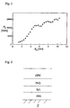
Es zeigen:
- Fig. 1:
- Ein Diagramm das die Abhängigkeit der Koerzitivkraft HC einer ferromagnetischen Schicht von der Dicke einer zugehörigen antiferrromagnetischen Schicht zeigt,
- Fig. 2:
- den grundlegenden Schichtaufbau eines erfndungsgemäßen Magnetfeldsensors,
- Fig. 3:
- den Magnetisierungsverlauf des in Fig. 2 dargestellten Schichtpakets eines Magnetfeldsensors über der äußeren Feldstärke H, bei großen Werten von H,
- Fig. 4:
- den Widerstandsverlauf im Magnetfeldsensor über der äußeren (detektierten) Feldstärke H, die kleiner ist als die Koerzitivfeldstärke HC2 einer FM2-Schicht,
- Fig. 5a, b:
- Varianten der Schichtenfolgen eines erfindungsgemäßen Sensors für mehrere Niveaus.
Beim Bau eines magnetoresistiven Sensors nach dem GMR-Prinzip muß gesichert sein, daß die Spininformation, die durch Leitungselektronen über die unmagnetische Zwischenschicht bzw. das Zwischenschichtpaket aus SpL- und AFM-Schicht übertragen wird, nicht verloren geht. Der Verlust der Spininformation wird dabei i.a. durch Streuprozesse in der Zwischenschicht hervorgerufen. Je weniger Streuprozesse in der Zwischenschicht stattfinden, desto höher ist der Anteil an Leitungselektronen, die die Spininformation zwischen der FM1- und der FM2-Schicht übertragen und desto höher ist damit auch die feldabhängige Änderung des Sensorwiderstands.
Die feldabhängige Änderung des Sensorwiderstands kann demnach sowohl durch eine relativ dicke Zwischenschicht als auch durch einen hohen spezifischen elektrischen Widerstand in der Zwischenschicht herabgesetzt werden, da sich in beiden Fällen die Anzahl der gestreuten Elektronen erhöht.
Claims (11)
- Magnetfeldsensor, bestehend aus einer Schichtenfolge von mindestens zwei ferromagnetischen Schichten (FM1, FM2, FMi), die durch eine unmagnetische Schicht voneinander getrennt sind, die so dünn ist, daß die Information über die relative Magnetisierungsrichtung der beiden ferromagnetischen Schichten zueinander in Form von spinpolarisierten Leitungselektronen übertragbar ist, wobei eine erste ferromagnetische Schicht (FM1) als Referenzschicht dient und wobei eine zweite ferromagnetische (FM2) eine antiferromagnetische Schicht (AFM) trägt,
dadurch gekennzeichnet, daß
die antiferromagnetische Schicht (AFM) aus einem aus mehreren atomaren Monolagen bestehenden antiferromagnetischen Material besteht, diese antiferromagnetische Schicht eine kubisch raumzentrierte Struktur und eine Kristallorientierung in (110)-Richtung aufweist, wobei die einzelnen magnetischen Momente in jeder Monolage zueinander antiferromagnetisch ausgerichtet sind und diese antiferromagnetische Schicht (AFM) eine derartige Dicke aufweist, daß eine magnetische Wechselwirkung mit der benachbarten ferromagnetischen Schicht (FM2) erfolgt, die zu einer Erhöhung der Koerzitivfeldstärke dieser ferromagnetischen Schicht führt, wobei über die Dicke der antiferromagnetischen Schicht (AFM) die Koerzitivfeldstärke dieser ferromagnetischen Schicht (FM2) über einen Bereich zwischen 200 A/m und 25000 A/m einstellbar ist. - Magnetfeldsensor nach Anspruch 1,
dadurch gekennzeichnet, daß
die Dicke (d) der antiferromagnetischen Schicht (AFM) > 2 nm beträgt. - Magnetfeldsensor nach Anspruch 1,
dadurch gekennzeichnet, daß
die Dicke (d) der antiferromagnetischen Schicht (AFM) vorzugsweise in einem Bereich von 2 nm < d < 12 nm liegt. - Magnetfeldsensor nach Anspruch 1,
dadurch gekennzeichnet, daß
die antiferromagnetische Schicht (AFM) aus Cr, Mn oder einer antiferromagnetischen Legierung besteht. - Magnetfeldsensor nach Anspruch 1,
dadurch gekennzeichnet, daß
dieser als Mehrniveausensor ausgebildet ist, der neben der ersten ferromagnetische Schicht (FM1) mehrere ferromagnetische Schichten (FMi) aufweist, wobei die ferromagnetischen Schichten (FM1, FMi) jeweils durch eine unmagnetische Schicht (SpLi) voneinander getrennt sind und jede der ferromagnetischen Schichten (FMi) eine antiferromagnetische Nachbarschicht (AFMi) von verschiedener Dicke trägt, wobei jede der ferromagnetischen Schichten (FMi) als Referenzschicht für die nächstfolgende ferromagnetische Schicht (FMi) dient und mindestens zwei der ferromagnetischen Schichten (FMi) unterschiedliche Koerzitivfelder aufweisen. - Magnetfeldsensor nach Anspruch 1,
dadurch gekennzeichnet, daß
dieser als Mehrniveausensor ausgebildet ist, der aus mehreren Schichtpaketen aufgebaut ist, wobei jedes Schichtpaket jeweils zwei ferromagnetische Schichten (FM1, FM2) aufweist, die durch eine unmagnetische Schicht (SpL1) voneinander getrennt sind und die ferromagnetischen Schichten (FM1, FM2) jeweils eine antiferromagnetische Nachbarschicht (AFM1, AFM2) von verschiedener Dicke tragen und mindestens zwei der ferromagnetischen Schichten (FM1, FM2) unterschiedliche Koerzitivfelder aufweisen. - Magnetfeldsensor nach Anspruch 1,
dadurch gekennzeichnet, daß
die Stromrichtung bei der Messung der Widerstandsänderung im Magnetfeldsensor parallel zu den Schichtebenen verläuft. - Magnetfeldsensor nach Anspruch 1,
dadurch gekennzeichnet, daß
die Stromrichtung bei der Messung der Widerstandsänderung im Magnetfeldsensor senkrecht zu den Schichtebenen verläuft. - Magnetfeldsensor nach Anspruch 1,
dadurch gekennzeichnet, daß
der Magnetfeldsensor derart ausgerichtet ist, daß das zu detektierende Magnetfeld vorzugsweise parallel zu den Schichtebenen verläuft. - Magnetfeldsensor nach Anspruch 1,
dadurch gekennzeichnet, daß
dieser eine einkristalline Struktur aufweist und die Magnetisierungsrichtungen der einzelnen ferromagnetischen Schichten aufgrund einer uniaxialen Symmetrie nur entlang einer Richtung in der Schichtebene zeigen, so daß der Sensor nur auf die Magnetfeldkomponente in dieser Richtung anspricht. - Magnetfeldsensor nach Anspruch 1,
dadurch gekennzeichnet, daß
dieser eine polykristalline Struktur aufweist, so daß er auf alle Magnetfelder, die in Schichtebene verlaufen, anspricht.
Applications Claiming Priority (3)
| Application Number | Priority Date | Filing Date | Title |
|---|---|---|---|
| DE19825392A DE19825392A1 (de) | 1998-05-28 | 1998-05-28 | Magnetfeldsensor |
| DE19825392 | 1998-05-28 | ||
| PCT/DE1999/001643 WO1999061930A1 (de) | 1998-05-28 | 1999-05-28 | Magnetfeldsensor |
Publications (2)
| Publication Number | Publication Date |
|---|---|
| EP1080375A1 EP1080375A1 (de) | 2001-03-07 |
| EP1080375B1 true EP1080375B1 (de) | 2003-07-23 |
Family
ID=7870173
Family Applications (1)
| Application Number | Title | Priority Date | Filing Date |
|---|---|---|---|
| EP99936411A Expired - Lifetime EP1080375B1 (de) | 1998-05-28 | 1999-05-28 | Magnetfeldsensor |
Country Status (5)
| Country | Link |
|---|---|
| EP (1) | EP1080375B1 (de) |
| AT (1) | ATE245818T1 (de) |
| AU (1) | AU5152299A (de) |
| DE (2) | DE19825392A1 (de) |
| WO (1) | WO1999061930A1 (de) |
Family Cites Families (4)
| Publication number | Priority date | Publication date | Assignee | Title |
|---|---|---|---|---|
| US5014147A (en) * | 1989-10-31 | 1991-05-07 | International Business Machines Corporation | Magnetoresistive sensor with improved antiferromagnetic film |
| US5373238A (en) * | 1992-11-06 | 1994-12-13 | International Business Machines Corporation | Four layer magnetoresistance device and method for making a four layer magnetoresistance device |
| JPH08221719A (ja) * | 1995-02-16 | 1996-08-30 | Tdk Corp | スピンバルブ磁気抵抗ヘッド及びその製造方法 |
| US5919580A (en) * | 1997-05-22 | 1999-07-06 | University Of Alabama | Spin valve device containing a Cr-rich antiferromagnetic pinning layer |
-
1998
- 1998-05-28 DE DE19825392A patent/DE19825392A1/de not_active Withdrawn
-
1999
- 1999-05-28 EP EP99936411A patent/EP1080375B1/de not_active Expired - Lifetime
- 1999-05-28 WO PCT/DE1999/001643 patent/WO1999061930A1/de not_active Ceased
- 1999-05-28 AU AU51522/99A patent/AU5152299A/en not_active Abandoned
- 1999-05-28 AT AT99936411T patent/ATE245818T1/de not_active IP Right Cessation
- 1999-05-28 DE DE59906363T patent/DE59906363D1/de not_active Expired - Fee Related
Also Published As
| Publication number | Publication date |
|---|---|
| ATE245818T1 (de) | 2003-08-15 |
| WO1999061930A1 (de) | 1999-12-02 |
| DE19825392A1 (de) | 1999-12-09 |
| AU5152299A (en) | 1999-12-13 |
| EP1080375A1 (de) | 2001-03-07 |
| DE59906363D1 (de) | 2003-08-28 |
Similar Documents
| Publication | Publication Date | Title |
|---|---|---|
| DE69130351T2 (de) | Verfahren zur Herstellung eines GMR Gegenstandes | |
| DE69106334T2 (de) | Mehrsicht Film mit magnetoresistiven Effekt und magnetoresitives Element. | |
| DE112012000741B4 (de) | Magnetische Stapel mit senkrechter magnetischer Anisotropie für einen magnetoresistiven Spin-Impuls-Transfer-Direktzugriffsspeicher | |
| DE69818884T2 (de) | Magnetoresistiver Sensor | |
| DE102019126320B4 (de) | Magnetoresistiver Sensor und Fertigungsverfahren für einen magnetoresistiven Sensor | |
| DE102007032867A1 (de) | Magnetoresistive Magnetfeldsensorstruktur | |
| DE102016102601B4 (de) | Magnetsensor | |
| DE112010002899T5 (de) | Verfahren zur Herstellung eines Magnetowiderstandseffektelements, eines Magnetsensors, einer Drehwinkel-Erfassungsvorrichtung | |
| DE19649265C2 (de) | GMR-Sensor mit einer Wheatstonebrücke | |
| DE102016105325A1 (de) | Magnetsensor | |
| EP0905523A2 (de) | Sensoreinrichtung zur Richtungserfassung eines äusseren Magnetfeldes mittels eines magnetoresistiven Sensorelementes | |
| DE4427495A1 (de) | Sensoreinrichtung mit einem GMR-Sensorelement | |
| DE102016111256B4 (de) | Magnetfeldgenerator, Magnetsensorsystem und Magnetsensor | |
| DE112012003852B4 (de) | Antiferromagnetische Speichereinheit | |
| DE19532674C1 (de) | Drehwinkelgeber unter Verwendung von Giant Magnetowiderstandsmaterialien | |
| EP1105890B1 (de) | Magnetoresistives element und dessen verwendung als speicherelement in einer speicherzellenanordnung | |
| DE4232244A1 (de) | Magnetowiderstands-Sensor | |
| EP3918356A1 (de) | Anordnung benachbarter schichtstrukturen für einen magnetoresistiven magnetfeldsensor, magnetoresistiver magnetfeldsensor und verfahren zu deren herstellung | |
| DE102005009390B3 (de) | Kraftsensor, Verfahren zur Ermittlung einer auf einen Kraftsensor wirkenden Kraft mittels eines Mehrschichtsystems aus magnetischen Schichten | |
| DE19742366C1 (de) | Einrichtung mit magnetoresistivem Sensorelement und zugeordneter Magnetisierungsvorrichtung | |
| EP0572465B1 (de) | Mehrschichtensystem für magnetoresistive sensoren und verfahren zu dessen herstellung | |
| DE102023202258A1 (de) | Magnetoresistiver sensor mit einem abschirmelement mit vortexmagnetisierung | |
| DE10036356C2 (de) | Magnetisches Dünnschichtbauelement | |
| DE4326999A1 (de) | Vorrichtung zum magnetfeldgesteuerten Schalten | |
| DE19825392A1 (de) | Magnetfeldsensor |
Legal Events
| Date | Code | Title | Description |
|---|---|---|---|
| PUAI | Public reference made under article 153(3) epc to a published international application that has entered the european phase |
Free format text: ORIGINAL CODE: 0009012 |
|
| 17P | Request for examination filed |
Effective date: 20001227 |
|
| AK | Designated contracting states |
Kind code of ref document: A1 Designated state(s): AT BE CH CY DE DK ES FI FR GB GR IE IT LI LU MC NL PT SE |
|
| 17Q | First examination report despatched |
Effective date: 20011213 |
|
| GRAH | Despatch of communication of intention to grant a patent |
Free format text: ORIGINAL CODE: EPIDOS IGRA |
|
| GRAH | Despatch of communication of intention to grant a patent |
Free format text: ORIGINAL CODE: EPIDOS IGRA |
|
| GRAA | (expected) grant |
Free format text: ORIGINAL CODE: 0009210 |
|
| AK | Designated contracting states |
Designated state(s): AT BE CH CY DE DK ES FI FR GB GR IE IT LI LU MC NL PT SE |
|
| PG25 | Lapsed in a contracting state [announced via postgrant information from national office to epo] |
Ref country code: NL Free format text: LAPSE BECAUSE OF FAILURE TO SUBMIT A TRANSLATION OF THE DESCRIPTION OR TO PAY THE FEE WITHIN THE PRESCRIBED TIME-LIMIT Effective date: 20030723 Ref country code: IT Free format text: LAPSE BECAUSE OF FAILURE TO SUBMIT A TRANSLATION OF THE DESCRIPTION OR TO PAY THE FEE WITHIN THE PRESCRIBED TIME-LIMIT;WARNING: LAPSES OF ITALIAN PATENTS WITH EFFECTIVE DATE BEFORE 2007 MAY HAVE OCCURRED AT ANY TIME BEFORE 2007. THE CORRECT EFFECTIVE DATE MAY BE DIFFERENT FROM THE ONE RECORDED. Effective date: 20030723 Ref country code: IE Free format text: LAPSE BECAUSE OF FAILURE TO SUBMIT A TRANSLATION OF THE DESCRIPTION OR TO PAY THE FEE WITHIN THE PRESCRIBED TIME-LIMIT Effective date: 20030723 Ref country code: GB Free format text: LAPSE BECAUSE OF FAILURE TO SUBMIT A TRANSLATION OF THE DESCRIPTION OR TO PAY THE FEE WITHIN THE PRESCRIBED TIME-LIMIT Effective date: 20030723 Ref country code: FR Free format text: LAPSE BECAUSE OF FAILURE TO SUBMIT A TRANSLATION OF THE DESCRIPTION OR TO PAY THE FEE WITHIN THE PRESCRIBED TIME-LIMIT Effective date: 20030723 Ref country code: FI Free format text: LAPSE BECAUSE OF FAILURE TO SUBMIT A TRANSLATION OF THE DESCRIPTION OR TO PAY THE FEE WITHIN THE PRESCRIBED TIME-LIMIT Effective date: 20030723 Ref country code: CY Free format text: LAPSE BECAUSE OF FAILURE TO SUBMIT A TRANSLATION OF THE DESCRIPTION OR TO PAY THE FEE WITHIN THE PRESCRIBED TIME-LIMIT Effective date: 20030723 |
|
| REG | Reference to a national code |
Ref country code: GB Ref legal event code: FG4D Free format text: NOT ENGLISH |
|
| REG | Reference to a national code |
Ref country code: CH Ref legal event code: EP |
|
| REG | Reference to a national code |
Ref country code: IE Ref legal event code: FG4D Free format text: GERMAN |
|
| REF | Corresponds to: |
Ref document number: 59906363 Country of ref document: DE Date of ref document: 20030828 Kind code of ref document: P |
|
| PG25 | Lapsed in a contracting state [announced via postgrant information from national office to epo] |
Ref country code: SE Free format text: LAPSE BECAUSE OF FAILURE TO SUBMIT A TRANSLATION OF THE DESCRIPTION OR TO PAY THE FEE WITHIN THE PRESCRIBED TIME-LIMIT Effective date: 20031023 Ref country code: GR Free format text: LAPSE BECAUSE OF FAILURE TO SUBMIT A TRANSLATION OF THE DESCRIPTION OR TO PAY THE FEE WITHIN THE PRESCRIBED TIME-LIMIT Effective date: 20031023 Ref country code: DK Free format text: LAPSE BECAUSE OF FAILURE TO SUBMIT A TRANSLATION OF THE DESCRIPTION OR TO PAY THE FEE WITHIN THE PRESCRIBED TIME-LIMIT Effective date: 20031023 |
|
| PG25 | Lapsed in a contracting state [announced via postgrant information from national office to epo] |
Ref country code: ES Free format text: LAPSE BECAUSE OF FAILURE TO SUBMIT A TRANSLATION OF THE DESCRIPTION OR TO PAY THE FEE WITHIN THE PRESCRIBED TIME-LIMIT Effective date: 20031103 |
|
| NLV1 | Nl: lapsed or annulled due to failure to fulfill the requirements of art. 29p and 29m of the patents act | ||
| PG25 | Lapsed in a contracting state [announced via postgrant information from national office to epo] |
Ref country code: PT Free format text: LAPSE BECAUSE OF FAILURE TO SUBMIT A TRANSLATION OF THE DESCRIPTION OR TO PAY THE FEE WITHIN THE PRESCRIBED TIME-LIMIT Effective date: 20031223 |
|
| GBV | Gb: ep patent (uk) treated as always having been void in accordance with gb section 77(7)/1977 [no translation filed] |
Effective date: 20030723 |
|
| REG | Reference to a national code |
Ref country code: IE Ref legal event code: FD4D |
|
| PG25 | Lapsed in a contracting state [announced via postgrant information from national office to epo] |
Ref country code: LU Free format text: LAPSE BECAUSE OF NON-PAYMENT OF DUE FEES Effective date: 20040528 Ref country code: AT Free format text: LAPSE BECAUSE OF NON-PAYMENT OF DUE FEES Effective date: 20040528 |
|
| PLBE | No opposition filed within time limit |
Free format text: ORIGINAL CODE: 0009261 |
|
| STAA | Information on the status of an ep patent application or granted ep patent |
Free format text: STATUS: NO OPPOSITION FILED WITHIN TIME LIMIT |
|
| PG25 | Lapsed in a contracting state [announced via postgrant information from national office to epo] |
Ref country code: MC Free format text: LAPSE BECAUSE OF NON-PAYMENT OF DUE FEES Effective date: 20040531 Ref country code: LI Free format text: LAPSE BECAUSE OF NON-PAYMENT OF DUE FEES Effective date: 20040531 Ref country code: CH Free format text: LAPSE BECAUSE OF NON-PAYMENT OF DUE FEES Effective date: 20040531 Ref country code: BE Free format text: LAPSE BECAUSE OF NON-PAYMENT OF DUE FEES Effective date: 20040531 |
|
| 26N | No opposition filed |
Effective date: 20040426 |
|
| EN | Fr: translation not filed | ||
| BERE | Be: lapsed |
Owner name: *HAHN-MEITNER-INSTITUT BERLIN G.M.B.H. Effective date: 20040531 |
|
| REG | Reference to a national code |
Ref country code: CH Ref legal event code: PL |
|
| PGFP | Annual fee paid to national office [announced via postgrant information from national office to epo] |
Ref country code: DE Payment date: 20080516 Year of fee payment: 10 |
|
| PG25 | Lapsed in a contracting state [announced via postgrant information from national office to epo] |
Ref country code: DE Free format text: LAPSE BECAUSE OF NON-PAYMENT OF DUE FEES Effective date: 20091201 |