EP1079613A2 - Image input apparatus - Google Patents
Image input apparatus Download PDFInfo
- Publication number
- EP1079613A2 EP1079613A2 EP00117316A EP00117316A EP1079613A2 EP 1079613 A2 EP1079613 A2 EP 1079613A2 EP 00117316 A EP00117316 A EP 00117316A EP 00117316 A EP00117316 A EP 00117316A EP 1079613 A2 EP1079613 A2 EP 1079613A2
- Authority
- EP
- European Patent Office
- Prior art keywords
- input apparatus
- image
- image input
- image formation
- array
- Prior art date
- Legal status (The legal status is an assumption and is not a legal conclusion. Google has not performed a legal analysis and makes no representation as to the accuracy of the status listed.)
- Withdrawn
Links
Images





Classifications
-
- H—ELECTRICITY
- H10—SEMICONDUCTOR DEVICES; ELECTRIC SOLID-STATE DEVICES NOT OTHERWISE PROVIDED FOR
- H10F—INORGANIC SEMICONDUCTOR DEVICES SENSITIVE TO INFRARED RADIATION, LIGHT, ELECTROMAGNETIC RADIATION OF SHORTER WAVELENGTH OR CORPUSCULAR RADIATION
- H10F39/00—Integrated devices, or assemblies of multiple devices, comprising at least one element covered by group H10F30/00, e.g. radiation detectors comprising photodiode arrays
- H10F39/80—Constructional details of image sensors
- H10F39/805—Coatings
-
- H—ELECTRICITY
- H04—ELECTRIC COMMUNICATION TECHNIQUE
- H04N—PICTORIAL COMMUNICATION, e.g. TELEVISION
- H04N25/00—Circuitry of solid-state image sensors [SSIS]; Control thereof
-
- H—ELECTRICITY
- H10—SEMICONDUCTOR DEVICES; ELECTRIC SOLID-STATE DEVICES NOT OTHERWISE PROVIDED FOR
- H10F—INORGANIC SEMICONDUCTOR DEVICES SENSITIVE TO INFRARED RADIATION, LIGHT, ELECTROMAGNETIC RADIATION OF SHORTER WAVELENGTH OR CORPUSCULAR RADIATION
- H10F39/00—Integrated devices, or assemblies of multiple devices, comprising at least one element covered by group H10F30/00, e.g. radiation detectors comprising photodiode arrays
- H10F39/011—Manufacture or treatment of image sensors covered by group H10F39/12
-
- H—ELECTRICITY
- H10—SEMICONDUCTOR DEVICES; ELECTRIC SOLID-STATE DEVICES NOT OTHERWISE PROVIDED FOR
- H10F—INORGANIC SEMICONDUCTOR DEVICES SENSITIVE TO INFRARED RADIATION, LIGHT, ELECTROMAGNETIC RADIATION OF SHORTER WAVELENGTH OR CORPUSCULAR RADIATION
- H10F39/00—Integrated devices, or assemblies of multiple devices, comprising at least one element covered by group H10F30/00, e.g. radiation detectors comprising photodiode arrays
- H10F39/011—Manufacture or treatment of image sensors covered by group H10F39/12
- H10F39/024—Manufacture or treatment of image sensors covered by group H10F39/12 of coatings or optical elements
-
- H—ELECTRICITY
- H10—SEMICONDUCTOR DEVICES; ELECTRIC SOLID-STATE DEVICES NOT OTHERWISE PROVIDED FOR
- H10F—INORGANIC SEMICONDUCTOR DEVICES SENSITIVE TO INFRARED RADIATION, LIGHT, ELECTROMAGNETIC RADIATION OF SHORTER WAVELENGTH OR CORPUSCULAR RADIATION
- H10F39/00—Integrated devices, or assemblies of multiple devices, comprising at least one element covered by group H10F30/00, e.g. radiation detectors comprising photodiode arrays
- H10F39/80—Constructional details of image sensors
- H10F39/806—Optical elements or arrangements associated with the image sensors
- H10F39/8063—Microlenses
-
- G—PHYSICS
- G02—OPTICS
- G02B—OPTICAL ELEMENTS, SYSTEMS OR APPARATUS
- G02B3/00—Simple or compound lenses
- G02B3/0006—Arrays
- G02B3/0012—Arrays characterised by the manufacturing method
- G02B3/0018—Reflow, i.e. characterized by the step of melting microstructures to form curved surfaces, e.g. manufacturing of moulds and surfaces for transfer etching
-
- G—PHYSICS
- G02—OPTICS
- G02B—OPTICAL ELEMENTS, SYSTEMS OR APPARATUS
- G02B3/00—Simple or compound lenses
- G02B3/0006—Arrays
- G02B3/0037—Arrays characterized by the distribution or form of lenses
- G02B3/0056—Arrays characterized by the distribution or form of lenses arranged along two different directions in a plane, e.g. honeycomb arrangement of lenses
Definitions
- the present invention relates to an image input apparatus that forms an image through a plurality of minute-image-formation optical systems.
- An arrangement conventionally known to help miniaturize an image input apparatus makes use of a lens array composed of a plurality of microlenses combined together. This is an application of the compound-eye seen in the visual system of insects, and helps realize an optical system that occupies less volume, offers a wider angle of view, and is brighter than a "single-eye" image formation system.
- Japanese Published Patent Application No. S59-50042 discloses an image input apparatus composed of a microlens array, a pinhole array, and an image surface.
- the microlenses form a reduced image of an object
- the pinholes paired one to one with the microlenses, sample different parts of this reduced image, forming together an image of the object on the image surface.
- Japanese Laid-Open Patent Application No. H5-100186 discloses an image input apparatus composed of a microlens array, a pinhole array, and a photosensitive element array.
- the microlenses, pinholes, and photosensitive elements are grouped into units each composed of a microlens, a pinhole, and a photosensitive element, and the individual units convert optical signals received from different parts of an object (subject) into electric signals, that together represent image information.
- Japanese Laid-Open Patent Application No. H10-107975 discloses an image input apparatus in which a plurality of photosensitive elements are arranged for each of microlenses.
- the image of an object formed by the microlenses is not sampled by pinholes that individually sample different parts thereof, but is directly read by a two-dimensionally extending photosensitive element array that yields signals of minute images.
- an aperture stop is arranged on the object side of the photosensitive element array and the microlens array, and the individual microlenses observe different parts of the object with no overlap among the signals obtained.
- the image input apparatuses disclosed in Japanese Published Patent Application No. S59-50042 and Japanese Laid-Open Patent Application No. H5-100186 mentioned above both have basically the same optical system, and suffer from unsatisfactory resolution in the image signals obtained.
- the number of units each including a microlens and a photosensitive element coincides with the number of dots, i.e. resolution, of the obtained image, therefore it is inevitable to increase the number of units to obtain a high-resolution image.
- the arrangement disclosed in Japanese Laid-Open Patent Application No. H10-107975 mentioned above solves the problem of unsatisfactory resolution in the image signals obtained, but, to obtain the best optical characteristics in this optical system, it is necessary to arrange the microlens array and the photosensitive element array on a spherical surface having its center at the aperture stop, and thus this arrangement is not fit for the purpose of making the entire image input apparatus satisfactorily compact.
- the individual photosensitive elements need to be arranged at discrete locations on a curved surface, i.e. a spherical surface in this case. This makes the photosensitive elements difficult to arrange in desired positions, and thus makes the entire image input apparatus difficult to manufacture.
- no aperture stop is used, and a microlens array and a photosensitive element array are each arranged on a flat plane.
- the photosensitive element array needs to be arranged at a certain distance from the microlens array, and thus the photosensitive element array requires an unduly large fitting area.
- this arrangement is specialized for narrow object angles at the cost of optical characteristics, and therefore exhibits various drawbacks in practical use.
- An object of the present invention is to provide an image input apparatus that has a simple construction, that is more compact than ever, and that offers high-resolution images.
- an image input apparatus is provided with: a photoelectric converter element having a flat photosensitive surface; and an image formation unit array having a plurality of image formation units arranged in an array.
- the plurality of image formation units individually receive light beams substantially from an identical area and focus the received light beams on different regions of the photosensitive surface of the photoelectric converter element to form images thereon.
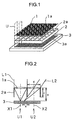
- FIG. 1 is an exploded perspective view schematically showing an image input apparatus embodying the invention.
- reference numeral 1 represents a microlens array having microlenses 1a arranged in a two-dimensional array, in a square shape for example
- reference numeral 3 represents a photosensitive element array disposed below the microlens array 1 so as to face it and having photosensitive elements 3a arranged similarly in a two-dimensional array, in a square shape for example
- Reference numeral 2 represents a partition wall layer disposed between microlens array 1 and photosensitive element array 3 and composed of partition walls 2a that are arranged below the boundaries of the individual microlenses 1a of the microlens array 1 so as to form a grid-like structure.
- one microlens 1a of the microlens array 1 corresponds to a plurality of photosensitive elements 3a of the photosensitive element array 3, and corresponds to one compartment formed in between in the partition wall layer 2.
- these together form a signal processing unit U.
- the individual units are separated from one another by the partition walls 2a to prevent the optical signal from one microlens 1a from entering the adjacent units; that is, the optical path through each unit is restricted.
- the photosensitive element array 3 it is possible to use a solid-state image-sensing device such as a CCD. This helps reduce the number of components needed and thereby simplify the construction of the image input apparatus.
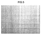
- Fig. 2 is a vertical sectional view schematically showing the optical systems of two adjacent ones among those units.
- the light beam L1 coming from the object as a rightful optical signal strikes the microlens 1a belonging to the unit U1 by traveling parallel to the optical axis X1 thereof. Then, the light beam is condensed by that microlens 1a on the photosensitive element array 3 belonging to the unit U1.
- a light beam L2 as an unnecessary optical signal, enters the adjacent unit U2 by traveling obliquely from a direction opposite to the target unit U1 at a large angle relative to the optical axis X2 of the microlens 1a belonging to the unit U2, this unnecessary light beam L2 also is focused on the photosensitive element array 3 belonging to the target unit U1.
- the partition walls 2a are provided between the units. It is needles to say that interference is perfectly prevented if the partition walls are formed so as to extend from the microlenses 1a to the photosensitive element array 3. However, even if the partition walls are formed partially, they effectively reduce unnecessary signals.
- microlens array the sizes of the whole microlens array and of each unit, the number of microlenses, the focal length, the manufacturing process will be presented below.
- two types of microlens array one using diffractive optical lenses and the other using refractive lenses, are presented.
- type using diffractive optical lenses two examples of different sizes are presented.
- ⁇ Diffractive Optical Lens Type Unit pitch 176 ⁇ m 250 ⁇ m
- Focal length 176 ⁇ m 250 ⁇ m
- Figs. 3A to 3D The manufacturing process of diffraction optical lenses is shown in Figs. 3A to 3D.
- a resist R is applied to the surface of a glass substrate G.
- an electron resist is used as this resist R.
- Fig. 3B by using an electron beam drawing machine, the desired pattern Pn is drawn on the resist R.
- Fig. 3C the drawn pattern is developed.
- Fig. 3D the drawn and developed pattern is transferred onto the glass substrate G by using an etching machine.
- the drawn pattern consists of Fresnel zone plates of either a binary or a multilevel type.
- Prototype lens arrays currently being manufactured have a minimum line width of 0.4 ⁇ m with binary-type zone plates and 0.2 ⁇ m with multilevel-type zone plates. When the minimum line width is as wide as about 1 ⁇ m, a laser beam can be used to draw the pattern.
- ⁇ Refractive Lens Type ⁇ Unit pitch 176 ⁇ m 250 ⁇ m
- Focal length about 230 ⁇ m about 350 ⁇ m
- Figs. 4A to 4D show the manufacturing process of refractive lenses.
- a so-called thermal re-flow method is applied here.
- a glass substrate G having a photo resist PR applied to its surface is coated with a mask M having a pattern drawn thereon.
- the glass substrate G is exposed to light from above as indicated by arrows W.
- the pattern is thus transferred onto the photo resist PR by so-called photolithography.
- the pattern consists not of Fresnel zone plates but of an array of circles that is used as a mask.
- the resist After exposure and then development, as shown in Fig. 4B, the resist remains as a pattern of cylindrical patches. As shown in Fig. 4C, when these remaining resist patches are post-baked by using a hotplate or an oven, they melt and form into the shapes of lenses by their own surface tension. As shown in Fig. 4D, by etching these resist patches, the resist patter is transferred onto the glass substrate G. Quartz is the typical material of the glass substrate G. The thermal re-flow method mentioned above is described in: "Micro-optics" by Hans Peter Herzig, p132-p136, published 1997 by Taylor & Francis.
- the partition walls are produced, for example, by cutting a metal with a laser, or by three-dimensionally molding a photo-setting resin.
- prototype partition walls having a thickness of 20 ⁇ m and arranged at intervals of 250 ⁇ m are produced from a stainless steel plate having a thickness of 200 ⁇ m.
- the surfaces of the partition walls are blackened.
- prototype partition walls are produced by scanning with a laser beam a resin called pentaerythritol triacrilate (PETA), which has a highly self-focusing property against light entering it, with 3% of benzil added thereto as a photopolymerization starter. It is confirmed that the partition walls thus produced have a thickness of about 56 ⁇ m and a height of about 500 ⁇ m.
- PETA pentaerythritol triacrilate
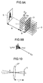
- Fig. 5 is a diagram of multiple reduced images formed by the lens array.
- the lens array used here is an array of gradient-index plane microlenses produced by ion exchange that have a focal length of 650 ⁇ m, have an aperture diameter of 250 ⁇ m, and are arranged at intervals of 250 ⁇ m.
- the photosensitive element used here is a CCD image-sensing device with 739 x 575 elements each having an aperture of 11 ⁇ m x 11 ⁇ m. In this case, approximately 22.7 x 22.7 elements constitute one unit. Although the number of elements that constitute one unit is not an integer number here, this does not affect the final image.
- Fig. 6 is a diagram showing an image reconstructed by gathering the signals obtained from the pixels at the centers of the units. As shown in this figure, an erect image of the object is obtained.
- Fig. 7 is a diagram showing an image reconstructed by using the signals obtained from all the photosensitive elements by an inverse matrix method. As shown in this figure, a satisfactory image is obtained.
- FIG. 8 is a perspective view schematically showing such polarizing filters.
- this polarizing filter array 4 is divided into blocks 4a each corresponding to one unit described above and has polarized light transmitting filters arranged in a checkered pattern such that every two adjacent filters have mutually perpendicular polarization directions.
- Two such polarizing filter arrays are prepared and arranged one at the microlens array surface and the other at the photosensitive element surface shown in Fig. 1 with each polarizing filter aligned with the corresponding unit.
- the filter blocks 4a adjacent thereto upward, downward, leftward, and rightward transmit only light polarized perpendicularly to the polarization direction of the filter block of the given unit.
- interference among the optical signals entering these adjacent units is prevented.
- polarizing filters either diffractive optical elements or hybrid elements, i.e. diffractive optical elements and refractive optical elements combined together, are used.
- the polarizing filters when composed of diffractive optical elements, is produced in the same manner as the diffractive lens array described above. That is, a resist pattern drawn by using an electric beam drawing machine is transferred onto a glass substrate by etching.
- the pattern of the polarizing filters is basically of a binary type consisting of lines and spaces. A minimum line width of approximately 0.2 ⁇ m can be obtained by using currently available electric beam drawing machine. Like the microlens array, when a relatively large minimum line width suffices, a laser beam drawing machine can be used.
- this image input apparatus is used when it is used as an image input apparatus that exhibits different sensitivities in different polarization directions.
- physical properties such as the dielectric constant
- To conduct measurement with a high sensitivity, accurate alignment and the like are necessary.
- Even with a comparatively simple image input apparatus it is possible to obtain general information regarding physical properties of an object. For example, when reflection occurs on the surface of a dielectric substance, it exhibits varying reflectances toward differently polarized light components. Thus, by observing polarization information, it is possible to know the angle of the reflecting surface relative to the image input apparatus.
- this technique can be applied in a measuring instrument for measuring the angle of a reflecting surface such as a glass plate.
- this technique can be applied to measurement of stress distribution inside a transparent object such as a plastic plane, or in an image input apparatus, such as a polarizing filter used in a camera, which acquires an object image by separating images reflected from and transmitted through a glass plate.
- the total thickness of an image input apparatus embodying the present invention depends on the following parameters: (Thickness of the Glass Substrate) + (Focal Length of the Microlenses) + (Thickness of the Photosensitive Elements)
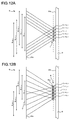
- Figs. 9A and 9B are perspective views schematically showing the configuration of the signal processing system for processing the optical signals acquired by an image input apparatus of the invention.
- the distance between the object 5 and the microlens array 1 is A
- the distance between the microlens array 1 and the photosensitive element array 3 is B
- the intervals at which the individual units are arranged is D.
- Reference symbol O represents the output signals obtained from the photosensitive element array 3.
- the numbers of the column and row in which a unit of the image input apparatus lies are represented by p and q
- the minute image in the unit [p, q] i.e.
- Fig. 9A in individual regions E on the photosensitive element array 3 (photoelectric converter element), images of the area (object 5) are formed as object images 5a seen from different view points.
- the images obtained in the individual units are object images 5a shifted by a predetermined distance from one another on the photosensitive element array 3 in accordance with the arrangement of the object 5, the microlens array 1, and the photosensitive element array 3.
- the microlens array 1 exerts no deflecting effect.
- the relative shift amount ⁇ in each unit is given by formula (3) below.
- ⁇ BD/A
- O p,q ⁇ I 0,0 (x-p ⁇ , y-q ⁇ ) f p,q (x, y) dxdy
- the obtained image signals can be processed in various ways.
- this can be achieved by specifying the addresses of the signals read out from the photosensitive element array.
- the output signals of the units they belong to it is possible to obtain output signals corresponding to formula (2).
- the procedure for achieving this is as follows. First, the partition walls are aligned with and then bonded to the microlens array, then the thus obtained integral unit is arranged in close contact with the surface of the photosensitive element array. In this state, the apparatus is already ready for use, but, to achieve more efficient use of the photosensitive element array and to facilitate post-processing, the above-mentioned integral unit is aligned with the photosensitive element array such that the partitions of the former are parallel with the regions of the latter.
- the pixels that output bright-state signals are regarded as effective pixels from which to read actual optical signals, and therefore, by using the positions of these pixels, it is possible to know the correspondence between the signals of the individual units and the addresses at which to read the outputs of the photosensitive elements. For example, unnecessary signals can be easily excluded by masking the other signals than those of the effective pixels after acquiring the data from all pixels.
- I p,q corresponds to the signal obtained from the photosensitive elements of the unit [p, q].
- I p,q represents the signals from the photosensitive elements except those located at the partition walls.
- I p,q represents the signals from the photosensitive elements excluding the photosensitive regions where interference is occurring.
- f p,q has finite sampling range and thus is a "rect" function, i.e. a function that gives "1" within the range corresponding to the regions (minute view angles) participating in image sensing and that gives "0" outside that range.
- a "rect" function i.e. a function that gives "1" within the range corresponding to the regions (minute view angles) participating in image sensing and that gives "0" outside that range.
- formula (c) the relationship between the width ⁇ of a pixel that senses light on the photosensitive element surface S and minute view angle ⁇ is given by formula (c) below.
- ⁇ 2 tan -1 ( ⁇ /2f) where f represents the focal length of an image formation element IF.
- the range of the rect function is determined by using this formula.
- Fig. 11 is a diagram schematically showing the relationship between the object and the field of view of the image input apparatus.
- This figure shows a case in which an image of an object 5 occupying an area extending over a length of X is formed on the photosensitive element array 3 through the microlenses L i, j .
- Inverted, reduced images of the entire object 5 are formed through the individual microlenses of the microlens array 1 on the corresponding regions of the photosensitive element array 3.
- the individual lenses of the microlens array 1 have different positional relationships with the object 5, the images formed on the individual regions of the photosensitive element array 3 have different information from one another. This is exploited to reconstruct an image.
- an image X of the entire object 5 is focused through each microlens L i,j of the microlens array 1, so as to form an image Z ( L i,j ) on the corresponding region of the photosensitive element array 3.
- the same number of inverted, reversed images of the object surface 5b on the object 5 as that of microlenses in the microlens array 1 are formed on the image formation surface 3b of photosensitive element array 3.
- the individual regions of the photosensitive element array corresponding one to one to the individual lenses have different positional relationships with the object 5, the images formed on the individual regions have different information as to the position of the image within the region, the intensity of the signal, and the like. This is exploited, for details, refer to the descriptions of Fig. 9A and Fig. 9B above.
- Figs. 12A and 12B are diagrams schematically showing the principle of making the field of view of the image input apparatus wider.
- each microlens L i,j of the microlens array 1 images a length of X i,j on the object plane 5b on the object 5 onto the image formation surface 3b of the photosensitive element array 3. Since the individual microlenses L i,j are located at different locations, they form images of different areas on the object surface 5b. As shown in Fig. 12 B, such differences are increased by the use of deflecting member, which thus helps make the overall field of view wider.
- a lens array 6 with a deflection function i.e. a functional optical element having both deflecting and image-forming functions is used.
- This lens array 6 has deflecting elements 6a provided one for each unit.
- the fields of view V of the individual units combine to cover a wider area on the object 5.
- Deflecting elements having such a deflecting function can be realized not only with prisms but also with diffracting optical elements. Their material, manufacturing process, size, and others are common to the diffractive lenses described earlier. Specifically, one method is to decenter the center of a pattern, such as Fresnel zone plate, that has an image-formation function in the direction in which to diffract the incident light. Another method is to overlay a one-dimensioned diffraction grating on an image-forming diffractive optical element. Both methods produce the same effects. When the deflection angle is relatively narrow, the former method is recommendable and when the deflection angle is relatively wide, the latter method is recommendable. How the field of view varies as a result of introduction of deflecting elements can be controlled by manipulating the parameters of each deflecting element.
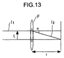
- Fig. 13 is a diagram schematically illustrating an example of the construction based on the former method described above.
- ⁇ represents the amount of decentering of the Fresnel zone plate F
- ⁇ represents the view angle
- f represents the focal length.
- Fig. 14 is a diagram schematically illustrating an example of the construction based on the latter method described above.
- d represents the grating constant of the one-dimensioned diffraction grating DG
- ⁇ represents the view angle
- ⁇ represents the wave length of the incident light.
- l 1 represents the incident light and l 2 represents the diffracted light.
- the decentering amount ⁇ and the grating constant d function as the above-mentioned parameters of each deflecting elements.
- the view angle ⁇ that each unit offers is equal to the deflection angle through which the incident light is deflected.
- Figs. 13 and 14 give formulae (a) and (b) below.
- ⁇ tan -1 ( ⁇ /f)
- ⁇ sin -1 (m ⁇ /d) where m represents an integer number.
- Fig. 15 is a perspective view schematically showing the construction of an image input apparatus employing a functional optical element to which a dispersive property is added.
- a functional optical element As shown in this diagram, which shows only a portion corresponding to one unit, as a functional optical element, a diffraction grating 7 is arranged above a photosensitive element array 3 so as to face it. Independent spectroscopes are formed one for each unit, so that the spectral data of different parts of the sensed object can be obtained.
- This diffraction grating 7 having different grating constants in the x and y directions indicated by arrows in the diagram, deflects the incoming light L at different angles according to the wave length, and then leads the resulting optical signal as spectral light La to the photosensitive elements 3a located at different locations on of the photosensitive element array 3.
- the photosensitive elements 3a constituting each unit are arranged in a square shape, and by deflecting the optical signals of the spectral light La in such a way as to cover all the area of that square, it is possible to make efficient use of the photosensitive elements 3a.
- the spectroscopes mentioned above are manufactured as diffractive optical elements just like the polarizing filters and deflecting elements described earlier. Therefore, they are produced from a quartz glass substrate by a similar manufacturing process.
- the pattern formed here is designed to have different predetermined grating constants in the x and y directions so that incident light is deflected at varying angles according to the wave length independently in each direction.
- Images obtained as a set of spectral data in this way have the following advantages and uses.
- an object is observed through a primary color filter when it is handed as visual information; however, more versatile information of the object can be obtained by using its spectral data.
- different materials have different spectral absorption coefficients, and therefore it is possible to identify the materials constituting the object and investigate their distribution by measuring the spectrum absorbed by the object.
- this technique can be applied to an apparatus which checks the level of comfortableness, mental state, and the like of a subject person by measuring the person's perspiration by using the wave length information of the light absorbed by water.
- Japanese Laid-Open Patent Application No. H8-184555 refer to Japanese Laid-Open Patent Application No. H8-184555.
Landscapes
- Engineering & Computer Science (AREA)
- Multimedia (AREA)
- Signal Processing (AREA)
- Facsimile Scanning Arrangements (AREA)
- Solid State Image Pick-Up Elements (AREA)
- Studio Devices (AREA)
- Image Input (AREA)
- Transforming Light Signals Into Electric Signals (AREA)
- Testing, Inspecting, Measuring Of Stereoscopic Televisions And Televisions (AREA)
- Color Television Image Signal Generators (AREA)
- Facsimile Heads (AREA)
Abstract
Description
| 〈〈Diffractive Optical Lens Type〉〉 | ||
| Unit pitch | 176 µm | 250 µm |
| Overall size | 8.8mm × 6.7mm (50 × 38 units) | 15mm × 15mm (60 × 60 units) |
| Focal length | 176 µm | 250 µm |
| 〈〈Refractive Lens Type〉〉 | ||
| Unit pitch | 176 µm | 250 µm |
| Overall size | 8.8mm × 6.7mm (50 × 38 units) | 15mm × 15mm (60 × 60 units) |
| Focal length | about 230 µm | about 350 µm |
Claims (9)
- An image input apparatus comprising:a photoelectric converter element having a flat photosensitive surface; andan image formation unit array having a plurality of image formation units arranged in an array,
wherein the plurality of image formation units individually receive light beams substantially from an identical area and focus the received light beam on different regions of the photosensitive surface of the photoelectric converter element to form images thereon. - An image input apparatus as claimed in claim 1,
wherein the individual images formed on the different regions are images of an object lying in the area as seen from different view points. - An image input apparatus as claimed in claim 1, further comprising:a restricting member for restricting, independently for each of the plurality of image formation units, optical paths along which the light beams are focussed.
- An image input apparatus as claimed in claim 3,
wherein the restriction member is realized as partition walls. - An image input apparatus as claimed in claim 4,
wherein those pixels of the photoelectric converter element which output a bright-state signal when light enters the plurality of image formation units are regarded as effective pixels. - An image input apparatus as claimed in claim 3,
wherein the restricting member is a polarizing filter array having polarizing filters arranged one for each group of the plurality of image formation units, every two adjacent polarizing filters having mutually perpendicular polarization angles. - An image input apparatus as claimed in claim 1, further comprising:deflecting members provided one for each of the plurality of image formation units.
- An image input apparatus as claimed in claim 1, further comprising:spectroscopic members provided one for each of the plurality of image formation units.
- An image input apparatus as claimed in claim 1, further comprising:a signal processing system for processing signals obtained as a result of photoelectric conversion performed by the photoelectric converter element by using processing functions provided one for each of the plurality of image formation units.
Applications Claiming Priority (2)
| Application Number | Priority Date | Filing Date | Title |
|---|---|---|---|
| JP23376099A JP3821614B2 (en) | 1999-08-20 | 1999-08-20 | Image input device |
| JP23376099 | 1999-08-20 |
Publications (2)
| Publication Number | Publication Date |
|---|---|
| EP1079613A2 true EP1079613A2 (en) | 2001-02-28 |
| EP1079613A3 EP1079613A3 (en) | 2008-05-28 |
Family
ID=16960155
Family Applications (1)
| Application Number | Title | Priority Date | Filing Date |
|---|---|---|---|
| EP00117316A Withdrawn EP1079613A3 (en) | 1999-08-20 | 2000-08-18 | Image input apparatus |
Country Status (3)
| Country | Link |
|---|---|
| US (1) | US7009652B1 (en) |
| EP (1) | EP1079613A3 (en) |
| JP (1) | JP3821614B2 (en) |
Cited By (18)
| Publication number | Priority date | Publication date | Assignee | Title |
|---|---|---|---|---|
| US6924935B2 (en) | 2003-10-23 | 2005-08-02 | Itt Manufacturing Enterprises Inc. | Compact multiple aperture imaging array |
| WO2005101805A1 (en) * | 2004-03-31 | 2005-10-27 | Eastman Kodak Company | Radiation image scanning apparatus and method |
| US7236304B2 (en) | 2003-11-04 | 2007-06-26 | Matsushita Electric Industrial Co., Ltd. | Imaging Device |
| EP1865713A2 (en) | 2006-06-08 | 2007-12-12 | Funai Electric Co., Ltd. | Compound-eye imaging device |
| EP1873559A1 (en) * | 2006-06-26 | 2008-01-02 | NEC Display Solutions Ltd | Illumination optics and projection display apparatus |
| WO2008006504A3 (en) * | 2006-07-10 | 2008-06-19 | Schott Ag | Method for producing optoelectronic components and correspondingly produced products |
| CN100473120C (en) * | 2004-10-28 | 2009-03-25 | 松下电器产业株式会社 | camera module |
| US7529383B2 (en) | 2002-10-25 | 2009-05-05 | Konica Minolta Holdings, Inc. | Image input apparatus |
| CN100520822C (en) * | 2005-01-20 | 2009-07-29 | 松下电器产业株式会社 | Lens array and image sensor provided with lens array |
| CN100553291C (en) * | 2003-12-18 | 2009-10-21 | 美光科技公司 | Color image sensor having array of imaging elements forming images on corresponding areas of sensor elements |
| WO2009154713A1 (en) * | 2008-06-19 | 2009-12-23 | Eastman Kodak Company | High dynamic range image sensor |
| EP2214405A2 (en) * | 2009-02-02 | 2010-08-04 | L-3 Communications Cincinnati Electronics | Multi-channel imaging devices |
| US7880794B2 (en) | 2005-03-24 | 2011-02-01 | Panasonic Corporation | Imaging device including a plurality of lens elements and a imaging sensor |
| US7894139B2 (en) | 2004-04-28 | 2011-02-22 | Panasonic Corporation | Imaging apparatus and method for manufacturing microlens array |
| EP2054850A4 (en) * | 2006-10-12 | 2011-06-15 | Ricoh Co Ltd | IMAGE ENTRY APPARATUS, IMAGE ENTRY METHOD, PERSONAL AUTHENTICATION APPARATUS, AND ELECTRONIC APPARATUS |
| EP2802009A1 (en) * | 2013-05-08 | 2014-11-12 | Ams Ag | Integrated imaging device for infrared radiation and method of production |
| EP3193368A1 (en) | 2016-01-13 | 2017-07-19 | ams AG | An optoelectronic device with a refractive element and a method of producing such an optoelectronic device |
| US10917546B2 (en) | 2016-07-29 | 2021-02-09 | Sony Semiconductor Solutions Corporation | Imaging device utilizing sensor area of photoelectric conversion elements corresponding to incident light passed through optical elements including a layer of polarizers of horizontal and vertical directions and quarter wave plates |
Families Citing this family (113)
| Publication number | Priority date | Publication date | Assignee | Title |
|---|---|---|---|---|
| JP2004032172A (en) * | 2002-06-24 | 2004-01-29 | Canon Inc | Compound-eye imaging device and device equipped with the same |
| US7567274B2 (en) * | 2002-12-09 | 2009-07-28 | Frank Edughom Ekpar | Method and apparatus for creating interactive virtual tours |
| US8031253B2 (en) * | 2003-06-24 | 2011-10-04 | Omnivision International Holding, Ltd. | Image sensor having micro-lens array separated with ridge structures and method of making |
| US8553113B2 (en) * | 2003-08-20 | 2013-10-08 | At&T Intellectual Property I, L.P. | Digital image capturing system and method |
| US7405761B2 (en) * | 2003-10-01 | 2008-07-29 | Tessera North America, Inc. | Thin camera having sub-pixel resolution |
| JP2006019918A (en) * | 2004-06-30 | 2006-01-19 | Matsushita Electric Ind Co Ltd | Imaging device |
| JP4411059B2 (en) * | 2003-12-12 | 2010-02-10 | キヤノン株式会社 | Display device with camera, communication device, and communication system |
| JP4616559B2 (en) * | 2004-01-15 | 2011-01-19 | 大日本印刷株式会社 | Display device and display system |
| DE102004003013B3 (en) * | 2004-01-20 | 2005-06-02 | Fraunhofer-Gesellschaft zur Förderung der angewandten Forschung e.V. | Optical imaging system for timepiece, portable computer, mobile telephone, spectacles, clothing item, chip card or sticker using array of optical channels with relatively angled optical axes |
| US8724006B2 (en) * | 2004-01-26 | 2014-05-13 | Flir Systems, Inc. | Focal plane coding for digital imaging |
| US7773143B2 (en) * | 2004-04-08 | 2010-08-10 | Tessera North America, Inc. | Thin color camera having sub-pixel resolution |
| US9819403B2 (en) | 2004-04-02 | 2017-11-14 | Rearden, Llc | System and method for managing handoff of a client between different distributed-input-distributed-output (DIDO) networks based on detected velocity of the client |
| US9826537B2 (en) | 2004-04-02 | 2017-11-21 | Rearden, Llc | System and method for managing inter-cluster handoff of clients which traverse multiple DIDO clusters |
| US10425134B2 (en) | 2004-04-02 | 2019-09-24 | Rearden, Llc | System and methods for planned evolution and obsolescence of multiuser spectrum |
| US8654815B1 (en) | 2004-04-02 | 2014-02-18 | Rearden, Llc | System and method for distributed antenna wireless communications |
| US8049806B2 (en) * | 2004-09-27 | 2011-11-01 | Digitaloptics Corporation East | Thin camera and associated methods |
| US8953087B2 (en) * | 2004-04-08 | 2015-02-10 | Flir Systems Trading Belgium Bvba | Camera system and associated methods |
| US20060055811A1 (en) * | 2004-09-14 | 2006-03-16 | Frtiz Bernard S | Imaging system having modules with adaptive optical elements |
| US7453653B2 (en) * | 2004-09-14 | 2008-11-18 | Omnivision Cdm Optics, Inc. | Low height imaging system and associated methods |
| KR100593896B1 (en) | 2004-12-27 | 2006-06-28 | 삼성전기주식회사 | Split Lens Camera Module |
| US10148897B2 (en) * | 2005-07-20 | 2018-12-04 | Rearden, Llc | Apparatus and method for capturing still images and video using coded lens imaging techniques |
| JP2006217131A (en) * | 2005-02-02 | 2006-08-17 | Matsushita Electric Ind Co Ltd | Imaging device |
| JP4807986B2 (en) * | 2005-09-05 | 2011-11-02 | 株式会社リコー | Image input device |
| JP2007116208A (en) | 2005-10-17 | 2007-05-10 | Funai Electric Co Ltd | Compound eye imaging apparatus |
| JP2007121631A (en) * | 2005-10-27 | 2007-05-17 | Funai Electric Co Ltd | Compound-eye imaging apparatus |
| US20070263114A1 (en) * | 2006-05-01 | 2007-11-15 | Microalign Technologies, Inc. | Ultra-thin digital imaging device of high resolution for mobile electronic devices and method of imaging |
| JP2007304525A (en) * | 2006-05-15 | 2007-11-22 | Ricoh Co Ltd | Image input apparatus, electronic apparatus, and image input method |
| JP4866147B2 (en) * | 2006-05-22 | 2012-02-01 | 株式会社リコー | Image shift detection method and apparatus, and image input apparatus |
| US7612319B2 (en) * | 2006-06-09 | 2009-11-03 | Aptina Imaging Corporation | Method and apparatus providing a microlens for an image sensor |
| KR100809277B1 (en) * | 2006-07-05 | 2008-03-03 | 삼성전기주식회사 | Camera Module with Array Lens |
| US8119502B2 (en) | 2006-07-10 | 2012-02-21 | Schott Ag | Method for packaging components |
| JP2008047587A (en) * | 2006-08-11 | 2008-02-28 | Sumitomo Electric Ind Ltd | Photodetector |
| CN101191885B (en) * | 2006-11-24 | 2011-07-27 | 鸿富锦精密工业(深圳)有限公司 | Array type camera module group |
| JP4954819B2 (en) * | 2007-07-23 | 2012-06-20 | リコー光学株式会社 | Blood vessel image input device and blood vessel image reading device |
| US8204282B2 (en) * | 2007-09-14 | 2012-06-19 | Ricoh Company, Ltd. | Image input device and personal authentication device |
| JP5067885B2 (en) * | 2007-09-14 | 2012-11-07 | 株式会社リコー | Image input device and personal authentication device |
| JP4640415B2 (en) | 2008-01-18 | 2011-03-02 | ソニー株式会社 | Biometric authentication device |
| JP4952598B2 (en) * | 2008-01-31 | 2012-06-13 | カシオ計算機株式会社 | Biometric authentication device |
| JP2009206922A (en) | 2008-02-28 | 2009-09-10 | Funai Electric Co Ltd | Compound-eye imaging apparatus |
| JP5293950B2 (en) | 2008-03-04 | 2013-09-18 | 株式会社リコー | Personal authentication device and electronic device |
| US20100028839A1 (en) * | 2008-07-18 | 2010-02-04 | Tully Timothy P | Methods and systems for evaluating memory agents |
| JP5105482B2 (en) * | 2008-09-01 | 2012-12-26 | 船井電機株式会社 | Optical condition design method and compound eye imaging apparatus |
| JP4748199B2 (en) | 2008-09-30 | 2011-08-17 | ソニー株式会社 | Vein imaging apparatus and vein imaging method |
| US20100283885A1 (en) * | 2009-05-11 | 2010-11-11 | Shih-Schon Lin | Method for aligning pixilated micro-grid polarizer to an image sensor |
| US20110026141A1 (en) | 2009-07-29 | 2011-02-03 | Geoffrey Louis Barrows | Low Profile Camera and Vision Sensor |
| JP2011176715A (en) * | 2010-02-25 | 2011-09-08 | Nikon Corp | Back-illuminated image sensor and imaging apparatus |
| DE102010031535A1 (en) * | 2010-07-19 | 2012-01-19 | Fraunhofer-Gesellschaft zur Förderung der angewandten Forschung e.V. | An image pickup device and method for picking up an image |
| GB2488519A (en) * | 2011-02-16 | 2012-09-05 | St Microelectronics Res & Dev | Multi-channel image sensor incorporating lenslet array and overlapping fields of view. |
| WO2013044149A1 (en) * | 2011-09-21 | 2013-03-28 | Aptina Imaging Corporation | Image sensors with multiple lenses of varying polarizations |
| JP5767929B2 (en) * | 2011-09-27 | 2015-08-26 | 株式会社東芝 | Solid-state imaging device and portable information terminal device |
| US8742527B2 (en) | 2011-09-27 | 2014-06-03 | Kabushiki Kaisha Toshiba | Solid state imaging device, solid state imaging element, portable information terminal device and method for manufacturing the solid state imaging element |
| JP2013074400A (en) * | 2011-09-27 | 2013-04-22 | Toshiba Corp | Solid-state image pickup device |
| JP5705140B2 (en) | 2011-09-27 | 2015-04-22 | 株式会社東芝 | Solid-state imaging device and method for manufacturing solid-state imaging device |
| US8854724B2 (en) | 2012-03-27 | 2014-10-07 | Ostendo Technologies, Inc. | Spatio-temporal directional light modulator |
| US8928969B2 (en) | 2011-12-06 | 2015-01-06 | Ostendo Technologies, Inc. | Spatio-optical directional light modulator |
| US8953083B2 (en) | 2012-02-13 | 2015-02-10 | Apple Inc. | Housing camera lens cover using GRIN technology |
| JP6089440B2 (en) * | 2012-04-26 | 2017-03-08 | 株式会社ニコン | Imaging device and imaging apparatus |
| JP6039567B2 (en) * | 2012-05-02 | 2016-12-07 | パナソニック インテレクチュアル プロパティ コーポレーション オブ アメリカPanasonic Intellectual Property Corporation of America | Solid-state imaging device |
| US9179126B2 (en) | 2012-06-01 | 2015-11-03 | Ostendo Technologies, Inc. | Spatio-temporal light field cameras |
| US9674436B2 (en) * | 2012-06-18 | 2017-06-06 | Microsoft Technology Licensing, Llc | Selective imaging zones of an imaging sensor |
| US9398229B2 (en) | 2012-06-18 | 2016-07-19 | Microsoft Technology Licensing, Llc | Selective illumination of a region within a field of view |
| US11189917B2 (en) | 2014-04-16 | 2021-11-30 | Rearden, Llc | Systems and methods for distributing radioheads |
| US9270876B2 (en) | 2013-01-05 | 2016-02-23 | The Lightco Inc. | Methods and apparatus for using multiple optical chains in parallel with multiple different exposure times |
| US9513470B1 (en) * | 2013-02-05 | 2016-12-06 | Vanderbilt University | Telecentric lens assembly providing a collimated light space |
| US10488535B2 (en) | 2013-03-12 | 2019-11-26 | Rearden, Llc | Apparatus and method for capturing still images and video using diffraction coded imaging techniques |
| US9973246B2 (en) | 2013-03-12 | 2018-05-15 | Rearden, Llc | Systems and methods for exploiting inter-cell multiplexing gain in wireless cellular systems via distributed input distributed output technology |
| US9923657B2 (en) | 2013-03-12 | 2018-03-20 | Rearden, Llc | Systems and methods for exploiting inter-cell multiplexing gain in wireless cellular systems via distributed input distributed output technology |
| RU2767777C2 (en) | 2013-03-15 | 2022-03-21 | Риарден, Ллк | Systems and methods of radio frequency calibration using the principle of reciprocity of channels in wireless communication with distributed input - distributed output |
| JP6189061B2 (en) * | 2013-03-19 | 2017-08-30 | 株式会社東芝 | Solid-state imaging device |
| US9557519B2 (en) | 2013-10-18 | 2017-01-31 | Light Labs Inc. | Methods and apparatus for implementing a camera device supporting a number of different focal lengths |
| US9374514B2 (en) * | 2013-10-18 | 2016-06-21 | The Lightco Inc. | Methods and apparatus relating to a camera including multiple optical chains |
| US9197816B2 (en) | 2013-10-18 | 2015-11-24 | The Lightco Inc. | Zoom related methods and apparatus |
| US9736365B2 (en) | 2013-10-26 | 2017-08-15 | Light Labs Inc. | Zoom related methods and apparatus |
| US9467627B2 (en) | 2013-10-26 | 2016-10-11 | The Lightco Inc. | Methods and apparatus for use with multiple optical chains |
| US9426365B2 (en) | 2013-11-01 | 2016-08-23 | The Lightco Inc. | Image stabilization related methods and apparatus |
| US9554031B2 (en) | 2013-12-31 | 2017-01-24 | Light Labs Inc. | Camera focusing related methods and apparatus |
| US9979878B2 (en) | 2014-02-21 | 2018-05-22 | Light Labs Inc. | Intuitive camera user interface methods and apparatus |
| US20150244949A1 (en) | 2014-02-21 | 2015-08-27 | Rajiv Laroia | Illumination methods and apparatus |
| US10191356B2 (en) | 2014-07-04 | 2019-01-29 | Light Labs Inc. | Methods and apparatus relating to detection and/or indicating a dirty lens condition |
| US10110794B2 (en) | 2014-07-09 | 2018-10-23 | Light Labs Inc. | Camera device including multiple optical chains and related methods |
| WO2016009707A1 (en) | 2014-07-16 | 2016-01-21 | ソニー株式会社 | Compound-eye imaging device |
| US9912864B2 (en) | 2014-10-17 | 2018-03-06 | Light Labs Inc. | Methods and apparatus for using a camera device to support multiple modes of operation |
| WO2016100756A1 (en) | 2014-12-17 | 2016-06-23 | The Lightco Inc. | Methods and apparatus for implementing and using camera devices |
| US9544503B2 (en) | 2014-12-30 | 2017-01-10 | Light Labs Inc. | Exposure control methods and apparatus |
| US10194098B2 (en) | 2015-01-28 | 2019-01-29 | Sony Corporation | Imaging apparatus and method of controlling imaging apparatus in which corresponding lines in partially overlapping images are sequentially exposed |
| US9824427B2 (en) | 2015-04-15 | 2017-11-21 | Light Labs Inc. | Methods and apparatus for generating a sharp image |
| US9857584B2 (en) | 2015-04-17 | 2018-01-02 | Light Labs Inc. | Camera device methods, apparatus and components |
| US9967535B2 (en) | 2015-04-17 | 2018-05-08 | Light Labs Inc. | Methods and apparatus for reducing noise in images |
| US10091447B2 (en) | 2015-04-17 | 2018-10-02 | Light Labs Inc. | Methods and apparatus for synchronizing readout of multiple image sensors |
| US10075651B2 (en) | 2015-04-17 | 2018-09-11 | Light Labs Inc. | Methods and apparatus for capturing images using multiple camera modules in an efficient manner |
| US9930233B2 (en) | 2015-04-22 | 2018-03-27 | Light Labs Inc. | Filter mounting methods and apparatus and related camera apparatus |
| US10129483B2 (en) | 2015-06-23 | 2018-11-13 | Light Labs Inc. | Methods and apparatus for implementing zoom using one or more moveable camera modules |
| US10491806B2 (en) | 2015-08-03 | 2019-11-26 | Light Labs Inc. | Camera device control related methods and apparatus |
| US10365480B2 (en) | 2015-08-27 | 2019-07-30 | Light Labs Inc. | Methods and apparatus for implementing and/or using camera devices with one or more light redirection devices |
| US9749549B2 (en) | 2015-10-06 | 2017-08-29 | Light Labs Inc. | Methods and apparatus for facilitating selective blurring of one or more image portions |
| US10003738B2 (en) | 2015-12-18 | 2018-06-19 | Light Labs Inc. | Methods and apparatus for detecting and/or indicating a blocked sensor or camera module |
| US10225445B2 (en) | 2015-12-18 | 2019-03-05 | Light Labs Inc. | Methods and apparatus for providing a camera lens or viewing point indicator |
| US10306218B2 (en) | 2016-03-22 | 2019-05-28 | Light Labs Inc. | Camera calibration apparatus and methods |
| CN106027861B (en) * | 2016-05-23 | 2019-06-04 | 西北工业大学 | Light field acquisition device and data processing method based on micro-camera array |
| US9948832B2 (en) | 2016-06-22 | 2018-04-17 | Light Labs Inc. | Methods and apparatus for synchronized image capture in a device including optical chains with different orientations |
| JP2019003976A (en) * | 2017-06-12 | 2019-01-10 | 大日本印刷株式会社 | Through electrode substrate, optical element, imaging module, imaging device |
| DE112017007695B4 (en) * | 2017-06-26 | 2026-01-15 | Mitsubishi Electric Corporation | COMPLETE EYE IMAGE DEVICE, IMAGE PROCESSING METHOD, PROGRAM AND RECORDING MEDIUM |
| JP6508385B2 (en) * | 2018-03-30 | 2019-05-08 | 株式会社ニコン | Imaging device and imaging device |
| US10916575B2 (en) | 2018-04-04 | 2021-02-09 | Samsung Electronics Co., Ltd. | Image sensor and method of manufacturing image sensor |
| US11030724B2 (en) | 2018-09-13 | 2021-06-08 | Samsung Electronics Co., Ltd. | Method and apparatus for restoring image |
| KR102680385B1 (en) | 2019-10-30 | 2024-07-02 | 삼성전자주식회사 | Method and device to restore multi lens image |
| KR102813299B1 (en) | 2019-12-24 | 2025-05-28 | 삼성전자주식회사 | Imaging device and image sensing method |
| US11595575B2 (en) | 2020-05-11 | 2023-02-28 | Samsung Electronics Co., Ltd. | Image sensor |
| CN112484853A (en) * | 2020-09-21 | 2021-03-12 | 厦门脉驰科技有限公司 | Method for eliminating signal light crosstalk in spectral analysis module based on optical filter array |
| KR102896028B1 (en) | 2020-10-22 | 2025-12-04 | 삼성전자주식회사 | Imaging device |
| KR20230037953A (en) | 2021-09-10 | 2023-03-17 | 삼성전자주식회사 | Method of color transform, electronic apparatus performing the method, and image sensor |
| KR20230059493A (en) | 2021-10-26 | 2023-05-03 | 삼성전자주식회사 | Method and apparatus for image processing using image synthesis based on feature matching |
| CN118603315B (en) * | 2023-12-06 | 2025-12-26 | 北京理工大学 | A compact imaging spectrometer for single-exposure imaging |
Family Cites Families (14)
| Publication number | Priority date | Publication date | Assignee | Title |
|---|---|---|---|---|
| US4323925A (en) * | 1980-07-07 | 1982-04-06 | Avco Everett Research Laboratory, Inc. | Method and apparatus for arraying image sensor modules |
| US4507197A (en) | 1982-08-09 | 1985-03-26 | Jim Walter Corporation | Apparatus and method for producing shot-free mineral wool |
| KR960000223B1 (en) * | 1990-11-16 | 1996-01-03 | 가부시키가이샤 도시바 | Solid state image device and method of manufacturing the same |
| JPH05100186A (en) | 1991-10-04 | 1993-04-23 | Omron Corp | Image sensor |
| US5703675A (en) * | 1992-01-17 | 1997-12-30 | Nikon Corporation | Projection-exposing apparatus with deflecting grating member |
| US5497269A (en) * | 1992-06-25 | 1996-03-05 | Lockheed Missiles And Space Company, Inc. | Dispersive microlens |
| JPH06244392A (en) * | 1993-02-17 | 1994-09-02 | Sharp Corp | Solid-state imaging device and manufacturing method thereof |
| DE59409779D1 (en) * | 1993-04-16 | 2001-07-19 | Infineon Technologies Ag | Diffractive optical device for the optical imaging of a spatial point on other spatial points |
| US5940126A (en) * | 1994-10-25 | 1999-08-17 | Kabushiki Kaisha Toshiba | Multiple image video camera apparatus |
| US6016224A (en) * | 1995-12-18 | 2000-01-18 | Olympus Optical Co., Ltd. | Multiple image optics system |
| DE69709709D1 (en) * | 1996-03-15 | 2002-02-21 | Retinal Display Cayman Ltd | METHOD AND DEVICE FOR VIEWING AN IMAGE |
| JP3622367B2 (en) | 1996-10-01 | 2005-02-23 | 松下電器産業株式会社 | Image input device |
| US6137535A (en) * | 1996-11-04 | 2000-10-24 | Eastman Kodak Company | Compact digital camera with segmented fields of view |
| NO305728B1 (en) | 1997-11-14 | 1999-07-12 | Reidar E Tangen | Optoelectronic camera and method of image formatting in the same |
-
1999
- 1999-08-20 JP JP23376099A patent/JP3821614B2/en not_active Expired - Lifetime
-
2000
- 2000-08-16 US US09/639,990 patent/US7009652B1/en not_active Expired - Lifetime
- 2000-08-18 EP EP00117316A patent/EP1079613A3/en not_active Withdrawn
Cited By (27)
| Publication number | Priority date | Publication date | Assignee | Title |
|---|---|---|---|---|
| US7529383B2 (en) | 2002-10-25 | 2009-05-05 | Konica Minolta Holdings, Inc. | Image input apparatus |
| US6924935B2 (en) | 2003-10-23 | 2005-08-02 | Itt Manufacturing Enterprises Inc. | Compact multiple aperture imaging array |
| US7236304B2 (en) | 2003-11-04 | 2007-06-26 | Matsushita Electric Industrial Co., Ltd. | Imaging Device |
| CN100553291C (en) * | 2003-12-18 | 2009-10-21 | 美光科技公司 | Color image sensor having array of imaging elements forming images on corresponding areas of sensor elements |
| WO2005101805A1 (en) * | 2004-03-31 | 2005-10-27 | Eastman Kodak Company | Radiation image scanning apparatus and method |
| US7480082B2 (en) | 2004-03-31 | 2009-01-20 | Carestream Health, Inc. | Radiation image scanning apparatus and method |
| US7894139B2 (en) | 2004-04-28 | 2011-02-22 | Panasonic Corporation | Imaging apparatus and method for manufacturing microlens array |
| CN100473120C (en) * | 2004-10-28 | 2009-03-25 | 松下电器产业株式会社 | camera module |
| CN100520822C (en) * | 2005-01-20 | 2009-07-29 | 松下电器产业株式会社 | Lens array and image sensor provided with lens array |
| US7880794B2 (en) | 2005-03-24 | 2011-02-01 | Panasonic Corporation | Imaging device including a plurality of lens elements and a imaging sensor |
| EP1865713A2 (en) | 2006-06-08 | 2007-12-12 | Funai Electric Co., Ltd. | Compound-eye imaging device |
| EP1865713A3 (en) * | 2006-06-08 | 2009-04-08 | Funai Electric Co., Ltd. | Compound-eye imaging device |
| US8348438B2 (en) | 2006-06-26 | 2013-01-08 | Nec Display Solutions, Ltd. | Illumination optics and projection display apparatus |
| EP1873559A1 (en) * | 2006-06-26 | 2008-01-02 | NEC Display Solutions Ltd | Illumination optics and projection display apparatus |
| US9027237B2 (en) | 2006-07-10 | 2015-05-12 | Schott Ag | Method for producing optoelectronic components, and products produced thereby |
| WO2008006504A3 (en) * | 2006-07-10 | 2008-06-19 | Schott Ag | Method for producing optoelectronic components and correspondingly produced products |
| EP2054850A4 (en) * | 2006-10-12 | 2011-06-15 | Ricoh Co Ltd | IMAGE ENTRY APPARATUS, IMAGE ENTRY METHOD, PERSONAL AUTHENTICATION APPARATUS, AND ELECTRONIC APPARATUS |
| WO2009154713A1 (en) * | 2008-06-19 | 2009-12-23 | Eastman Kodak Company | High dynamic range image sensor |
| US7964840B2 (en) | 2008-06-19 | 2011-06-21 | Omnivision Technologies, Inc. | High dynamic range image sensor including polarizer and microlens |
| EP2214405A2 (en) * | 2009-02-02 | 2010-08-04 | L-3 Communications Cincinnati Electronics | Multi-channel imaging devices |
| EP2802009A1 (en) * | 2013-05-08 | 2014-11-12 | Ams Ag | Integrated imaging device for infrared radiation and method of production |
| WO2014180635A1 (en) * | 2013-05-08 | 2014-11-13 | Ams Ag | Integrated imaging device for infrared radiation and method of production |
| US9577001B2 (en) | 2013-05-08 | 2017-02-21 | Ams Ag | Integrated imaging device for infrared radiation and method of production |
| DE112014002312B4 (en) | 2013-05-08 | 2019-05-23 | Ams Ag | Integrated infrared radiation imaging device and manufacturing method |
| EP3193368A1 (en) | 2016-01-13 | 2017-07-19 | ams AG | An optoelectronic device with a refractive element and a method of producing such an optoelectronic device |
| US10644047B2 (en) | 2016-01-13 | 2020-05-05 | Ams Ag | Optoelectronic device with a refractive element and a method of producing such an optoelectronic device |
| US10917546B2 (en) | 2016-07-29 | 2021-02-09 | Sony Semiconductor Solutions Corporation | Imaging device utilizing sensor area of photoelectric conversion elements corresponding to incident light passed through optical elements including a layer of polarizers of horizontal and vertical directions and quarter wave plates |
Also Published As
| Publication number | Publication date |
|---|---|
| JP2001061109A (en) | 2001-03-06 |
| US7009652B1 (en) | 2006-03-07 |
| EP1079613A3 (en) | 2008-05-28 |
| JP3821614B2 (en) | 2006-09-13 |
Similar Documents
| Publication | Publication Date | Title |
|---|---|---|
| US7009652B1 (en) | Image input apparatus | |
| Duparré et al. | Micro-optical artificial compound eyes | |
| US5801831A (en) | Fabry-Perot spectrometer for detecting a spatially varying spectral signature of an extended source | |
| US6124974A (en) | Lenslet array systems and methods | |
| CN103472592B (en) | A snapshot high-throughput polarization imaging method and polarization imager | |
| US5859420A (en) | Optical imaging device | |
| JP5646445B2 (en) | Thin camera with sub-pixel resolution | |
| US5659420A (en) | Confocal optical apparatus | |
| US5438366A (en) | Aspherical blur filter for reducing artifacts in imaging apparatus | |
| US5299275A (en) | Optical fiber filter for reducing artifacts in imaging apparatus | |
| CN101147392B (en) | Imaging device and lens array used therein | |
| US4467195A (en) | Information detecting apparatus | |
| US5615048A (en) | Imaging system | |
| JPH01237619A (en) | Optical apparatus | |
| JPH0617981B2 (en) | Method and apparatus for use in producing autostereoscopic images | |
| KR20000064348A (en) | Video sensor | |
| CN101384945A (en) | Optically multiplexed imaging systems and methods of operation | |
| US5684293A (en) | Anti-aliasing low-pass blur filter for reducing artifacts in imaging apparatus | |
| EP0883013A2 (en) | Phase-noise type broad spectral bandwidth optical low-pass anti-aliasing filter | |
| JPH06130321A (en) | Optical device for splitting real image | |
| JP4532968B2 (en) | Focus detection device | |
| JPH10210213A (en) | Optical device | |
| US12607456B2 (en) | Wide field-of-view metasurface optics, sensors, cameras and projectors | |
| EP0518362B1 (en) | Image display device using liquid-crystal panel, liquid-crystal TV projector, and conical optical-element array used therein | |
| JP2019082412A (en) | Imaging apparatus |
Legal Events
| Date | Code | Title | Description |
|---|---|---|---|
| PUAI | Public reference made under article 153(3) epc to a published international application that has entered the european phase |
Free format text: ORIGINAL CODE: 0009012 |
|
| AK | Designated contracting states |
Kind code of ref document: A2 Designated state(s): AT BE CH CY DE DK ES FI FR GB GR IE IT LI LU MC NL PT SE |
|
| AX | Request for extension of the european patent |
Free format text: AL;LT;LV;MK;RO;SI |
|
| PUAL | Search report despatched |
Free format text: ORIGINAL CODE: 0009013 |
|
| AK | Designated contracting states |
Kind code of ref document: A3 Designated state(s): AT BE CH CY DE DK ES FI FR GB GR IE IT LI LU MC NL PT SE |
|
| AX | Request for extension of the european patent |
Extension state: AL LT LV MK RO SI |
|
| RAP1 | Party data changed (applicant data changed or rights of an application transferred) |
Owner name: KONICA MINOLTA HOLDINGS, INC. Owner name: MINOLTA CO., LTD. |
|
| RAP1 | Party data changed (applicant data changed or rights of an application transferred) |
Owner name: KONICA MINOLTA HOLDINGS, INC. |
|
| 17P | Request for examination filed |
Effective date: 20080930 |
|
| 17Q | First examination report despatched |
Effective date: 20081121 |
|
| AKX | Designation fees paid |
Designated state(s): DE FR GB |
|
| STAA | Information on the status of an ep patent application or granted ep patent |
Free format text: STATUS: THE APPLICATION IS DEEMED TO BE WITHDRAWN |
|
| 18D | Application deemed to be withdrawn |
Effective date: 20090602 |