JP4411059B2 - Display device with camera, communication device, and communication system - Google Patents
Display device with camera, communication device, and communication system Download PDFInfo
- Publication number
- JP4411059B2 JP4411059B2 JP2003415820A JP2003415820A JP4411059B2 JP 4411059 B2 JP4411059 B2 JP 4411059B2 JP 2003415820 A JP2003415820 A JP 2003415820A JP 2003415820 A JP2003415820 A JP 2003415820A JP 4411059 B2 JP4411059 B2 JP 4411059B2
- Authority
- JP
- Japan
- Prior art keywords
- display
- display device
- camera
- imaging
- image
- Prior art date
- Legal status (The legal status is an assumption and is not a legal conclusion. Google has not performed a legal analysis and makes no representation as to the accuracy of the status listed.)
- Expired - Fee Related
Links
- 238000004891 communication Methods 0.000 title claims description 18
- 238000003384 imaging method Methods 0.000 claims description 72
- 230000003287 optical effect Effects 0.000 claims description 26
- 239000000758 substrate Substances 0.000 claims description 16
- 239000011159 matrix material Substances 0.000 claims description 8
- 238000006243 chemical reaction Methods 0.000 claims description 6
- 230000002194 synthesizing effect Effects 0.000 claims description 4
- 238000005401 electroluminescence Methods 0.000 claims description 2
- 230000005540 biological transmission Effects 0.000 description 13
- 239000011521 glass Substances 0.000 description 12
- 238000000034 method Methods 0.000 description 12
- 238000010586 diagram Methods 0.000 description 10
- 238000007789 sealing Methods 0.000 description 6
- 239000003086 colorant Substances 0.000 description 3
- 150000001875 compounds Chemical class 0.000 description 3
- 230000008921 facial expression Effects 0.000 description 3
- 239000000853 adhesive Substances 0.000 description 2
- 230000001070 adhesive effect Effects 0.000 description 2
- 229910052782 aluminium Inorganic materials 0.000 description 2
- XAGFODPZIPBFFR-UHFFFAOYSA-N aluminium Chemical compound [Al] XAGFODPZIPBFFR-UHFFFAOYSA-N 0.000 description 2
- 239000002274 desiccant Substances 0.000 description 2
- 230000006866 deterioration Effects 0.000 description 2
- 239000004973 liquid crystal related substance Substances 0.000 description 2
- 229910021420 polycrystalline silicon Inorganic materials 0.000 description 2
- 229920005591 polysilicon Polymers 0.000 description 2
- 241000282412 Homo Species 0.000 description 1
- XUIMIQQOPSSXEZ-UHFFFAOYSA-N Silicon Chemical compound [Si] XUIMIQQOPSSXEZ-UHFFFAOYSA-N 0.000 description 1
- WGLPBDUCMAPZCE-UHFFFAOYSA-N Trioxochromium Chemical compound O=[Cr](=O)=O WGLPBDUCMAPZCE-UHFFFAOYSA-N 0.000 description 1
- 230000002159 abnormal effect Effects 0.000 description 1
- NIXOWILDQLNWCW-UHFFFAOYSA-N acrylic acid group Chemical group C(C=C)(=O)O NIXOWILDQLNWCW-UHFFFAOYSA-N 0.000 description 1
- 230000002411 adverse Effects 0.000 description 1
- 230000008033 biological extinction Effects 0.000 description 1
- 230000015572 biosynthetic process Effects 0.000 description 1
- 229910000423 chromium oxide Inorganic materials 0.000 description 1
- 230000006835 compression Effects 0.000 description 1
- 238000007906 compression Methods 0.000 description 1
- 230000006837 decompression Effects 0.000 description 1
- 239000006185 dispersion Substances 0.000 description 1
- 230000000694 effects Effects 0.000 description 1
- 239000010408 film Substances 0.000 description 1
- 230000004907 flux Effects 0.000 description 1
- 230000001771 impaired effect Effects 0.000 description 1
- 239000000463 material Substances 0.000 description 1
- 229910052751 metal Inorganic materials 0.000 description 1
- 239000002184 metal Substances 0.000 description 1
- 239000000203 mixture Substances 0.000 description 1
- 239000011368 organic material Substances 0.000 description 1
- 229920001296 polysiloxane Polymers 0.000 description 1
- 238000003672 processing method Methods 0.000 description 1
- 239000011347 resin Substances 0.000 description 1
- 229920005989 resin Polymers 0.000 description 1
- 230000004043 responsiveness Effects 0.000 description 1
- 229910052710 silicon Inorganic materials 0.000 description 1
- 239000010703 silicon Substances 0.000 description 1
- GGCZERPQGJTIQP-UHFFFAOYSA-N sodium;9,10-dioxoanthracene-2-sulfonic acid Chemical compound [Na+].C1=CC=C2C(=O)C3=CC(S(=O)(=O)O)=CC=C3C(=O)C2=C1 GGCZERPQGJTIQP-UHFFFAOYSA-N 0.000 description 1
- 239000010409 thin film Substances 0.000 description 1
Images


Classifications
-
- H—ELECTRICITY
- H04—ELECTRIC COMMUNICATION TECHNIQUE
- H04N—PICTORIAL COMMUNICATION, e.g. TELEVISION
- H04N7/00—Television systems
- H04N7/14—Systems for two-way working
- H04N7/141—Systems for two-way working between two video terminals, e.g. videophone
- H04N7/142—Constructional details of the terminal equipment, e.g. arrangements of the camera and the display
- H04N7/144—Constructional details of the terminal equipment, e.g. arrangements of the camera and the display camera and display on the same optical axis, e.g. optically multiplexing the camera and display for eye to eye contact
-
- H—ELECTRICITY
- H04—ELECTRIC COMMUNICATION TECHNIQUE
- H04N—PICTORIAL COMMUNICATION, e.g. TELEVISION
- H04N23/00—Cameras or camera modules comprising electronic image sensors; Control thereof
- H04N23/50—Constructional details
- H04N23/54—Mounting of pick-up tubes, electronic image sensors, deviation or focusing coils
-
- H—ELECTRICITY
- H04—ELECTRIC COMMUNICATION TECHNIQUE
- H04N—PICTORIAL COMMUNICATION, e.g. TELEVISION
- H04N25/00—Circuitry of solid-state image sensors [SSIS]; Control thereof
-
- H—ELECTRICITY
- H04—ELECTRIC COMMUNICATION TECHNIQUE
- H04N—PICTORIAL COMMUNICATION, e.g. TELEVISION
- H04N7/00—Television systems
- H04N7/14—Systems for two-way working
- H04N7/141—Systems for two-way working between two video terminals, e.g. videophone
- H04N7/142—Constructional details of the terminal equipment, e.g. arrangements of the camera and the display
- H04N2007/145—Handheld terminals
Landscapes
- Engineering & Computer Science (AREA)
- Multimedia (AREA)
- Signal Processing (AREA)
- Two-Way Televisions, Distribution Of Moving Picture Or The Like (AREA)
- Devices For Indicating Variable Information By Combining Individual Elements (AREA)
- Studio Devices (AREA)
- Control Of El Displays (AREA)
- Indication In Cameras, And Counting Of Exposures (AREA)
- Electroluminescent Light Sources (AREA)
- Control Of Indicators Other Than Cathode Ray Tubes (AREA)
Description
本発明は、テレビ電話、テレビ会議などに利用されるディスプレイ装置に関し、さらに詳しくは、撮像機能を有するディスプレイ装置およびこれを用いた通信装置に関する。 The present invention relates to a display device used for a videophone, a video conference, and the like, and more particularly to a display device having an imaging function and a communication device using the same.
テレビ電話やテレビ会議などに利用されるディスプレイ装置には、相手側のディスプレイに表示するために自己の映像を撮影するカメラと、相手側で撮影された相手の映像を表示するディスプレイとから構成され、ディスプレイで相手と対面しながら通話できるものがある。 A display device used for a videophone or a video conference is composed of a camera that takes a picture of itself for display on the other party's display and a display that displays the other person's picture taken by the other party. , There is something that can talk while facing the other party on the display.
このようなディスプレイ装置では、ディスプレイで相手と対面したときに、ディスプレイに表示される相手の映像と目線が合うように構成されることで、相手と実際に対面しているように通話を行うことができる(例えば、特許文献1,2参照)。 In such a display device, when facing the other party on the display, it is configured so that the line of sight of the other party's video displayed on the display matches, thereby making a call as if actually facing the other party (For example, see Patent Documents 1 and 2).
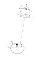
図12は、従来のテレビ会議用ディスプレイ装置が利用される状況を説明した図であり、図13は、その光学的な構成を説明した図である。 FIG. 12 is a diagram illustrating a situation in which a conventional video conference display device is used, and FIG. 13 is a diagram illustrating an optical configuration thereof.
図12において、1は平面型ディスプレイであり、不図示のパーソナルコンピューター(以下PCと称す)に接続される。1bは画面であり、通信状態では相手側の顔や、会話に使用されるドキュメント類が必要に応じて画面内に分割されて表示される。このような構成は、インターネット等通信回線につながった通常のPC環境で実現される。 In FIG. 12, reference numeral 1 denotes a flat display, which is connected to a personal computer (not shown) (hereinafter referred to as a PC). Reference numeral 1b denotes a screen. In the communication state, the other party's face and documents used for conversation are divided and displayed in the screen as necessary. Such a configuration is realized in a normal PC environment connected to a communication line such as the Internet.
また、2はテーブルである。3は自己の映像を相手に送るためのビデオカメラであり、図13に示すような光学系が内蔵されている。このビデオカメラ3は、顔4と画面1bとの間には無く、画面1bの下側で人間4が画面1bを見る際の視野外に位置している。
また、図13において、3aはビデオカメラ3に内蔵された撮像用レンズ(実際には複数のレンズで構成されているが説明を簡略化するために図中1枚のレンズで示している)であり、3bはビデオカメラ3に内蔵されている撮像素子である。5は撮像素子3b上の人間4の像である。
In FIG. 13, reference numeral 3a denotes an imaging lens built in the video camera 3 (actually, it is composed of a plurality of lenses, but is shown as a single lens in the figure for the sake of simplicity). Yes, 3b is an image sensor incorporated in the
このような構成では、人間4の仮想平面を表す線Aは、レンズ3aを通して平面Cのように投影される。これは、レンズ3aの光軸と垂直な面Bを特定すると、この各軸A、B、Cの延長線が一点で交わるという「シャインプルーフの法則」である。 In such a configuration, the line A representing the virtual plane of the human 4 is projected like the plane C through the lens 3a. This is the “Scheinproof law” in which when the plane B perpendicular to the optical axis of the lens 3a is specified, the extended lines of the axes A, B, and C intersect at one point.
このような構成より得られるセンサ3b上の画像はあご側の撮影倍率が高く(近い距離であるゆえ)頭頂側の撮影倍率が低い(遠距離)物になり、あまり好ましくない画像となる。
しかしながら、上記した従来例には、テレビ受像機などで主流になりつつある平面型のディスプレイ、携帯電話やモバイル、パソコンなどに適した薄型のディスプレイにおいて、デザインを損なわないようにし、かつ、人物の表情が判別できるように解像度を高くするという提案はなかった。 However, in the above-described conventional example, the flat display, which is becoming mainstream in television receivers, and the like in thin displays suitable for mobile phones, mobiles, personal computers, etc. There was no proposal to increase the resolution so that facial expressions could be identified.
また、第一の課題として、ディスプレイに映る映像を見ている人の目線はディスプレイの略中央部にいっており、この人の目線を撮像するには、同じディスプレイの中央部と同じところに光軸を持つカメラを設定しなければならず、これはともすると表示装置としての性能、品位を損なうことになる。この欠点を補うために、画面のごく近傍にカメラを取り付ける例も考えられるがこれらは逆に目線が捕らえられず、あるいは顔を斜めから見たような画像になってしまう。 Also, as a first issue, the eye of the person watching the image on the display is in the approximate center of the display. To capture this person's eye, light is emitted in the same area as the center of the same display. A camera with an axis must be set, which would impair the performance and quality of the display device. In order to make up for this drawback, there may be an example in which a camera is attached in the very vicinity of the screen. However, in this case, the line of sight is not captured, or the image looks as if the face is viewed from an oblique direction.
第二の課題として、カメラには人の顔を中心にして多少の周辺風景を撮像するような構図で、かつ、物の表情が判別できるような高い解像度を持つような焦点距離が求められているが、このような撮影倍率の光学系を平面ディスプレイの装置の中に組み込むと厚みが増してしまいせっかくの平面ディスプレイのデザインが損なわれる。 The second issue is that the camera is required to have a focal length that has a composition that captures some of the surrounding scenery centered on the person's face and that has a high resolution that can distinguish the facial expression of objects. However, if an optical system with such a magnification is incorporated into a flat display device, the thickness increases and the design of the flat display is impaired.
第三の課題として、相手の表情を見ている最中にこちらの画像も撮像することが求められており(リアルタイム性)、このような場合、表示用の光が撮像系のゴーストやフレアーになりやすく、画質の劣化が起こることがある。 As a third problem, it is required to capture this image while looking at the other's facial expression (in real time). In such a case, the display light is sent to the ghost or flare of the imaging system. The image quality is likely to deteriorate.
そこで、本発明は、ディスプレイを見ている人物をほぼ正面から撮像できる薄型のカメラ付きディスプレイ装置を提供することを目的としている。 Therefore, an object of the present invention is to provide a thin display device with a camera that can image a person who is looking at the display from almost the front.
上記の目的を達成するために、本発明のカメラ付きディスプレイ装置は、ブラックマトリックス部を有する表示画素が配列された表示素子と、表示素子における表示画素の間に形成された複数の開口(アパーチャ)領域を通して複数の物体像を形成し、該複数の物体像を光電変換する撮像モジュールと、撮像モジュールを用いて得られた複数の物体像の画像データを合成する画像合成手段とを有し、開口領域に隣接する表示画素のブラックマトリックス部が前記撮像モジュールに対する開口絞りを構成し、前記複数の開口領域の中心と前記撮像モジュールを結ぶ撮像光軸が前記表示素子に対して物体側の位置にて交差する。
To achieve the above object, a camera-equipped display device of the present invention includes a display device displaying pixels having a black matrix portion are arranged, a plurality of apertures (aperture formed between the display pixels in Table示素Ko ) An imaging module that forms a plurality of object images through the region, photoelectrically converts the plurality of object images, and an image combining unit that combines image data of the plurality of object images obtained using the imaging module; black matrix of the display pixels adjacent to the opening region constitutes the aperture stop to the previous SL imaging module, positioned on the object side to the imaging optical axis connecting the imaging module and the center of the plurality of open regions is the display device Cross at
本発明によれば、表示画素の間に形成された複数の開口(アパーチャ)領域を通して形成された複数の物体像を光電変換することにより得られた画像データを合成して画像を得るので、ディスプレイを見ている人物(観察者)に目立たないかたちで、しかも該観察者をほぼ正面から撮像することができる。これにより、携帯電話やテレビ電話(会議)システムを快適な状態で行うことが可能となる。 According to the present invention, an image is obtained by synthesizing image data obtained by photoelectrically converting a plurality of object images formed through a plurality of aperture (aperture) regions formed between display pixels. It is possible to take an image of the observer from the front almost inconspicuously to the person (observer) who is watching. Thereby, it becomes possible to perform a mobile phone and a videophone (conference) system in a comfortable state.
さらに本発明によれば、いわゆる複眼撮像モジュールを構成することになり、1つ1つの開口領域が小さくても全体として広い撮像画角を得ることができる。したがって、短い焦点距離で、すなわち薄い空間に十分入る構造で撮像モジュールを構成することが可能となり、撮像モジュールの内蔵によってディスプレイ装置が厚くなることを防止できる。
さらに、複数の撮像用レンズの光軸が、表示素子に対して物体側の位置(例えば、観察者の顔の位置)にて交差するようにすることで(かつ、各物体像を撮像する撮像センサ領域の画素を物体の位置で空間的にずらすことで)、当該位置の被写体を高解像度で撮像することができる。
Furthermore, according to the present invention, a so-called compound-eye imaging module is formed, and a wide imaging angle of view can be obtained as a whole even if each opening area is small. Therefore, it is possible to configure the imaging module with a short focal length, that is, a structure that sufficiently enters a thin space, and it is possible to prevent the display device from becoming thick due to the built-in imaging module.
Further, the optical axes of a plurality of imaging lenses intersect with the display element at a position on the object side (for example, the position of the face of the observer) (and imaging for capturing each object image). By spatially shifting the pixels in the sensor area at the position of the object, the subject at that position can be imaged with high resolution.
また、表示素子(ディスプレイ)の画面中央部から外れた位置に上記開口領域を配置することにより、観察者の注視点から撮像位置をずらすことが可能になり、複数の撮像(画像)データの合成画像を作ることにより、あたかもディスプレイ画面の中心から撮像した画像のように見せることができる。
In addition, by arranging the opening area at a position off the center of the screen of the display element ( display ) , it is possible to shift the imaging position from the observer's gazing point, and to synthesize a plurality of imaging (image) data. By creating an image, it can appear as if it were taken from the center of the display screen.
また、本発明によれば、ディスプレイの表示タイミングと撮像タイミングを交互にずらして連続的に駆動することにより、ディスプレイ側からの光による撮像画像の劣化を防止できる。 Further, according to the present invention, it is possible to prevent deterioration of the captured image due to light from the display side by alternately driving the display timing and imaging timing of the display alternately.
以下、本発明に係る実施例について図1から図11を参照して説明する。なお、本実施例の構成は本発明を実施する上での例にすぎず、本発明が本実施例の構成に限定されるものではない。以下の説明において、上記した従来例と同様の構成を有する部材には同一の符号を付す。本実施例では、本発明に係るディスプレイ装置の一形態として、携帯電話を例に用いて説明する。 Embodiments according to the present invention will be described below with reference to FIGS. The configuration of the present embodiment is merely an example for carrying out the present invention, and the present invention is not limited to the configuration of the present embodiment. In the following description, members having the same configurations as those of the conventional example described above are denoted by the same reference numerals. In this embodiment, a mobile phone will be described as an example of a display device according to the present invention.
図3は、本実施の形態に係る携帯電話(通信装置)の使用状況の説明図である。 図3に示すように、本実施例の携帯電話は、ディスプレイ部1にカメラ3が内蔵されている。このカメラ3は人物4の目線や顔の方向に向けて配置されている。
FIG. 3 is an explanatory diagram of the usage status of the mobile phone (communication device) according to the present embodiment. As shown in FIG. 3, the mobile phone of this embodiment has a
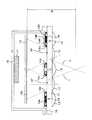
図1および図2は、本実施例に係る携帯電話のディスプレイ部1の断面図である。なお、図1は、本発明の実施例1であるディスプレイ部を、図2は、本発明の実施例2であるディスプレイ部の断面図である。
1 and 2 are sectional views of the display unit 1 of the mobile phone according to the present embodiment. 1 is a cross-sectional view of a display unit that is Embodiment 1 of the present invention, and FIG. 2 is a cross-sectional view of the display unit that is
図1および図2に示すように、ディスプレイ部1は、画面を表面側に形成するガラス基板11と、該ガラス基板11の背面側に一画素ごとに形成され一画素ごとに異なる色を発光可能な有機EL(エレクトロルミネセンス)素子14と、ガラス基板の背面側を封止する封止缶16と、を有する。
As shown in FIG. 1 and FIG. 2, the display unit 1 is capable of emitting a different color for each pixel formed on the
ガラス基板11には、反射防止膜や低温ポリシリコンによるTFT(薄膜トランジスタ)による回路が形成される等の下処理がなされている。また、該ガラス基板11には、アクリルなどの樹脂でできているレプリカレンズ12,13が一体的に形成されている。
The
ここで、図1は、ガラス基板11における後述する有機EL素子14(表示画素)が形成された面にレプリカレンズ12を形成した例を、図2は、ガラス基板11における有機EL素子14が形成された面とは反対側(外側)の面にレプリカレンズ12,13を形成した例を示す。
Here, FIG. 1 shows an example in which the
レプリカレンズ12は撮像用レンズであり、後述のセンサ基板15に形成されているセンサ部に被写界(図中下側)の像を結像するように構成される。また、レプリカレンズ13は、後述の有機EL素子14の発光光束を集光するための集光用レンズである。
The
また、有機EL素子14は、ガラス基板11に形成される低温ポリシリコンの透明な回路によって一画素ごとに駆動され、一画素ごとに異なる色が点灯又は消灯されるものである。各有機EL素子14の駆動を制御することでディスプレイ全体として一つの画像が表示される。さらに、有機EL素子は点灯、消灯のスピードが従来の液晶などに比べて3桁以上速く、本実施の形態に特に好適なものである。
The
該有機EL素子14は、反射板とコモン電極として使用されるアルミ反射板14aと、ブルー、グリーン、レッド各色の発光をする有機材料でできたEL層14B、14G、14Rと、ブラックマトリックスとして各画素のコントラストをあげたり、漏洩光を防止したりするための酸化クロムなどでできているブラックマトリックス部14cとを有する。
The
なお、ブラックマトリックス部14cは、撮像用レンズ12の絞りとしても機能していて(一体に作られていて)、それは図中14dで示されているように、ゴーストの発生を防止するナイフエッジ形状に構成されている。
Note that the
そして、本実施例では、撮像用レンズ12は、有機EL素子14(すなわち表示画素)の間に形成された複数の開口領域APごとに配置されている。
In this embodiment, the
また、撮像用レンズ12の焦点がほぼ結ばれる位置にはセンサ基板15が設けられている。該センサ基板(以下、撮像センサという)15は、不図示の固定構造により不図示の回路部と後述の封止缶16に接合され、センサ面15aと駆動回路が一体的に形成されている。そして、該撮像センサ15のセンサ面15aに撮像用レンズ12の焦点位置がほぼ結ぶように構成される。
In addition, a
また、センサ面15aに形成された複数のセンサ領域の画像処理上の画像中心とレプリカレンズ12の中心とを結ぶ、いわゆる光軸Lが、この画面を観察する人間4(図3参照)がいると思われる位置(図中、センサ面15aから距離D離れた位置)でほぼ交差するように構成されている。
In addition, there is a human 4 (see FIG. 3) who observes this screen with a so-called optical axis L that connects the image center of the plurality of sensor regions formed on the
また、前記封止缶16は、封止用の金属で構成され、耐湿性の高い接着剤18によってガラス基板11に固着される。そして、封止缶16の一部には乾燥剤17が固着される。これは、有機EL素子14が空気中の水分に反応してダークスポットと呼ばれる非発光部が生じないように、空気中の水分を除去するものである。また、このような構成によれば、従来の液晶ディスプレイ装置よりもさらに薄いフラットディスプレイ装置を提供することができる。
The sealing can 16 is made of a sealing metal and is fixed to the
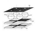
図4から図6は、本実施例のディスプレイ装置に用いられる撮像モジュールを説明するための図である。 4 to 6 are diagrams for explaining an imaging module used in the display apparatus of the present embodiment.
該撮像モジュールの光学系にはいわゆる複眼光学系が用いられ、図5に示すように、4つの撮像レンズ12により形成された物体像を互いに独立した4つの撮像センサ15上に結像させ、得られた4つの画像データから一つの画像を合成することで、高画質な像データを作成する。
A so-called compound eye optical system is used as the optical system of the imaging module. As shown in FIG. 5, the object images formed by the four
図6は、光学系と撮像センサの断面図であり、(a)は本実施例に係る複眼光学系の構造であり、図6(b)は従来の光学系の構造である。 6A and 6B are cross-sectional views of the optical system and the image sensor. FIG. 6A shows the structure of the compound eye optical system according to the present embodiment, and FIG. 6B shows the structure of the conventional optical system.
図6(a)において、12は撮像用のレプリカレンズであり、15はセンサである。上記した図1及び図2と同様の構成である。 In FIG. 6A, 12 is a replica lens for imaging, and 15 is a sensor. The configuration is the same as in FIGS. 1 and 2 described above.
図6(b)には、本実施例の光学系と同じ性能を出すための従来の光学系が示されており、21はレンズ群、22は撮像センサである。該撮像センサ22は、カラーフィルタがベイヤー配列(市松状に配列されている)されたものである。
FIG. 6B shows a conventional optical system for producing the same performance as the optical system of the present embodiment, in which 21 is a lens group, and 22 is an image sensor. The
図6(b)に示す従来の光学系では、レンズ群21を見てわかるように、可視光の3原色である青、緑、赤(以下B、G、Rと呼ぶ)の各波長の光を同じセンサ面に結像するために色消しと呼ばれる手法が用いられる。すなわち、単レンズでは波長の異なる光を同じ平面に結像できないため、3種の屈折と分散(波長による屈折の違い)が異なるレンズを使ってこれらの3原色を同一平面状に結像させる。このために図で示すようにレンズユニットの厚みが必要となる。このレンズユニットの色消し構造を通称アポクロマートと呼ぶ。
In the conventional optical system shown in FIG. 6B, as can be seen from the
また、通常の撮像系に用いられる撮像センサ22の大きさは、例えばVGA(640×480=約30万画素)の場合、1画素のサイズが4μ角であると仮定すると2.56×1.92mmとなる。
Further, the size of the
一方で、本実施例のように、色ごとに光学系を異ならせた複眼光学系を使うと1.28×0.96mmの撮像センサ15を4つ使うことになる。但し、1つの撮像センサ15の受光範囲を複数に分割して各撮像用レンズ12により形成される物体像に割り当てるようにしてもよい。
On the other hand, if a compound eye optical system with different optical systems for each color is used as in this embodiment, four 1.28 × 0.96
このように、画面サイズが異なる場合それに使用する光学系は、例えば銀塩カメラの標準的な画角θであるf=38mmレンズに相当するレンズが、通常の光学系における2.56×1.92mmのセンサだとf=2.6mmのレンズユニット21となる。一方で、本実施例の光学系における1.28×0.96mmのセンサであると、その半分のf=1.3mmの撮像用レンズ12を用いればよい。すなわち、本実施例では、通常の光学系に比較して、レンズおよび撮像センサを含めた撮像光学系の厚みを約半分とすることができる。
As described above, when the screen sizes are different, an optical system used for the lens corresponds to, for example, an f = 38 mm lens having a standard angle of view θ of a silver salt camera, which is 2.56 × 1. If the sensor is 92 mm, the
また、焦点距離が半分になるとD=f/Fno.なる原理式により同じ明るさのレンズの直径も略半分となり表示機の各表示画素の間にこの撮像用レンズを埋め込んでも目立たなくなる。(4つのレンズの面積を加えるとほぼ従来タイプのレンズの開口の大きさと等しくなる。)また、レンズが観察者の注視点部である画面の中心から外れることで観察画像の劣化が目立たなくなり、本発明の目的である通話者同士の視線を合わせる(ディスプレイを見ている観察者をほぼ正面から撮像する)ということに好適な構成とすることができる。 When the focal length is halved, D = f / Fno. According to this principle formula, the diameter of the lens having the same brightness is substantially halved, and even if this imaging lens is embedded between each display pixel of the display device, it becomes inconspicuous. (When the area of the four lenses is added, it becomes almost the same as the size of the aperture of the conventional type lens.) Also, the deterioration of the observation image becomes inconspicuous because the lens is off the center of the screen which is the gazing point of the observer. A configuration suitable for aligning the line of sight of the callers, which is the object of the present invention (taking an image of an observer who is looking at the display from almost the front), can be achieved.
図5は、本実施例の撮像モジュールの構造を示す斜視図である。 図5において、12は前述の撮像用レンズであり、上記したガラス基板11にレプリカ成形されている。該撮像用レンズ12は、画面の中央部の4箇所に配置される。23はカラーフィルタであり、各レンズに入った白色光のうち各撮像センサ15に必要な波長(色)のみをそれぞれの撮像センサ15に入射させるものである。24はガラス基板11に印刷された絞りである。
FIG. 5 is a perspective view showing the structure of the imaging module of the present embodiment. In FIG. 5,
図4は、撮影画像の処理方法の説明図であり、(a)は4つのレンズで撮影された4つの像を示す図、(b)は(a)の4つの像を電気的に重ねあわせた像を示す図、(c)は詳細図である。 FIGS. 4A and 4B are explanatory diagrams of a method for processing captured images, where FIG. 4A is a diagram illustrating four images captured by four lenses, and FIG. 4B is a diagram of electrically superimposing the four images of FIG. FIG. 4C is a detailed view showing a captured image.
本実施例では、4つの撮像用レンズ12から入射した光により形成される物体像を電気信号に変換して読み出すときに、例えば図4(a)の第二象限部にあるセンサの一番右上の画像の次に、第一象限部の一番右上の画像、第三象限部の一番右上の画像、第四象限部の一番右上の画像、次に第二象限部の右から二番目の画像・・・のように交互に読み出す回路によって、図4(b)のような通常のベイヤー配列と同等の映像信号を作り出している。
In the present embodiment, when an object image formed by light incident from the four
図7は、本実施の形態のディスプレイにおける撮像用レンズ12の配置の一例を示す正面図である。
FIG. 7 is a front view showing an example of the arrangement of the
図7において、12は撮像用レンズであり、13はディスプレイ光の集光(表示)用レンズである。なお、本図では、集光用レンズ13を画面中心部にしか描いていないが、実際は画面全体に配置されている。
In FIG. 7, 12 is an imaging lens, and 13 is a lens for condensing (displaying) display light. In this figure, although the condensing
撮像用レンズ12は、集光用レンズ13に対し、図中四角で示す画面の中央部に略均等にばら撒かれて配置されており、サイズが小さいこととあいまって、ディスプレイ画面を見る者にとって気にならない構成である。
The
図8は、本実施例のディスプレイにおける撮像用レンズ12の配置の他の例を示すもので、図8(a)はディスプレイの正面図であり、(b)はディスプレイの使用状況を示す側面図である。
FIG. 8 shows another example of the arrangement of the
図8(a)において、4つで1組の撮像用レンズ12(すなわち、4つの撮像モジュール)は、図中に四角で示すディスプレイ画面の中央部と、画面を四分割した領域の各中央部(四隅部)との合計5箇所に配置される。また、集光用レンズ13は、画面全体に敷き詰められているが図8(a)では省略して中心部のみ描かれている。
In FIG. 8A, a set of four imaging lenses 12 (that is, four imaging modules) includes a central portion of a display screen indicated by a square in the drawing and each central portion of a region obtained by dividing the screen into four. It is arranged at a total of five places (four corners). The condensing
そして、図8(b)に示すように、四隅の撮像モジュールの撮像光軸(図中一点鎖線で示す)Lは、画面から距離D(すなわち画面と人物との距離、例えば30から50cm)ほど離れた人物の方向を向くように設定される。 As shown in FIG. 8B, the imaging optical axes (indicated by the alternate long and short dash lines in the figure) L of the imaging module at the four corners are about a distance D from the screen (that is, the distance between the screen and the person, for example, 30 to 50 cm). It is set to face the direction of a distant person.
このような構成は、複数の場所、または複数の人物と通話をするときに、4つに分割した画面(分割される画面の領域は4つに限定されない)それぞれに異なる場所や人物が表示されるような場合を想定したものである。 In such a configuration, when talking to a plurality of places or a plurality of persons, different places and persons are displayed on each of the four divided screens (the area of the divided screen is not limited to four). This is assumed.
例えば、画面中央部に共通のドキュメント資料などを配置し、相手の映像は画面全体の1/4位の位置に表示するようなテレビ会議の設定や、パソコンなど据え置き型のテレビ電話システムに適する。 For example, it is suitable for a video conference setting in which a common document material or the like is arranged in the center of the screen and the other party's video is displayed at a position of 1/4 of the entire screen, or a stationary videophone system such as a personal computer.
また、自分の顔を四隅の画面の通信している人物に向けるだけで、現在どの場所、人物と話しているかをパソコンが自動的に判別してそのカメラからの撮像画像を相手先などに選択的に送ることも可能である。 Also, simply point your face to the person who is communicating on the screens at the four corners, and the computer will automatically determine where you are talking to and the person you are talking to, and select the captured image from that camera as the other party. Can also be sent.
図11は、本実施例に係る携帯電話の制御回路図である。図11において、31は送受信のデジタル信号を高速で変換するDSPIであり、マイコン32へ受信信号を変換して伝達すると同時に、マイコン32からの送信信号を逆にデジタルの送信信号に変換する。DSPIには画像や音声の圧縮機能や解凍機能が内蔵される。
FIG. 11 is a control circuit diagram of the mobile phone according to the present embodiment. In FIG. 11,
33はDSPIIであり、マイコン32で分離された送受信の画像信号のみを高速にディスプレイ装置を駆動するのに適した信号に変換、あるいは後述のディスプレイ40にある不図示の撮像モジュールのエリアセンサ(シリコンセンサ15a)からのデジタル信号をマイコンに変換、伝達する。
34、35はそれぞれ発信ユニット、受信ユニットであり、36、37はそれぞれマイクユニット、スピーカーユニットである。
38はカメラコントローラーとしてカメラ部をコントロールするものであり、39はディスプレイコントローラーとして有機EL表示部をコントロールするものである。
38 is intended to control the camera section as a
このディスプレイ40のカメラ(撮像モジュール)部及び及び表示部は、図10に示すように、マイコン32によって時系列にコントロールされている。
The camera (imaging module) part and display part of the
図10において、受信ユニット35から得られた受信信号は、DSPI31及びマイコン32によって高速に変換され、DSPII33及びディスプレイコントローラー39を介して、ディスプレイ40の有機EL素子を駆動する。このときに信号を変換するタイミング(受信信号変換タイミング)が図10のAで示され、有機EL素子を駆動するタイミング(受信画像表示タイミング)が図10のBに示される。
In FIG. 10, the received signal obtained from the receiving
また、図10に示すCはカメラの撮像が行われているタイミング(送信画像撮像タイミング)を示している。図10に示すDはカメラで撮像した画像をDSPII33で画像信号に変換し、この画像信号をマイコン32及びDSPI31によって送信信号にリアルタイムで変換し発信ユニット34によって送信するタイミング(送信信号変換タイミング)を示している。
Further, C shown in FIG. 10 indicates the timing at which the camera is capturing (transmission image capturing timing). D shown in FIG. 10 converts an image captured by the camera into an image signal by the
このような構成によれば、有機EL素子の発光タイミングBが、送信画像撮影タイミングCと完全にずれているため、有機EL素子からの発光が、内蔵されている撮像モジュールによる撮像に悪影響を与えないように駆動される。
According to such a configuration, since the light emission timing B of the organic EL element is completely deviated from the transmission image capturing timing C, the light emission from the organic EL element has an adverse effect on imaging by the built-in imaging module. Not to be driven.
有機EL素子は、このような発光、消灯の応答性が必要な使用方法に非常に適したものである。 The organic EL element is very suitable for a usage method that requires such responsiveness of light emission and extinction.
また、図10中“S”で示すインターバルは、画像のちらつきが人間にわからないように1/30秒とすることが理想的である。なお、送受信のデータ量、及び、データの変換のスピードを考慮して、1/10から1/15秒くらいとしてもよい。
In addition, the interval indicated by “S” in FIG. 10 is ideally 1/30 seconds so that humans do not notice the flickering of the image. In consideration of the amount of data to be transmitted and received and the speed of data conversion, it may be 1/10 to 1/15 seconds.
図9は、本実施例における通信システムのフローチャートを示す図である。各ステップに符号を付して説明する。 FIG. 9 is a diagram illustrating a flowchart of the communication system in the present embodiment. Each step will be described with reference numerals.
図9において、S101では、携帯電話への着信が開始する。S102では、ユーザーによってフックアップボタンが押される。 In FIG. 9, in S101, the incoming call to the mobile phone starts. In S102, the hookup button is pressed by the user.
S103では、信号が受信されたか否かを確認する。信号が受信されるとS104に進み、信号が受信されないとS109に進む。 In S103, it is confirmed whether or not a signal is received. If a signal is received, the process proceeds to S104, and if no signal is received, the process proceeds to S109.
S104では、マイコン32によって受信信号に基づいて画像を表示するタイミングか否かが確認される。すなわち、カウンターによるカウントが0の場合、画像を表示するタイミングと判断してS105に進む。
In S104, it is confirmed by the
S105からS107では、受信信号がDSPI31、DSPII33、及びマイコン32などを介して変換され、ディスプレイ40に映像表示され、スピーカーユニット37に音声出力される。
In S <b> 105 to S <b> 107, the received signal is converted via the
その後、S108では、前述のカウンターを1に変更後、再度S104に戻る。 Thereafter, in S108, the above-described counter is changed to 1, and the process returns to S104 again.
一方、S104でカウントが1の場合、撮像を行うタイミングと判断してS109に進む。 On the other hand, when the count is 1 in S104, it is determined that it is time to perform imaging, and the process proceeds to S109.
S109では、信号が受信されたか否かを確認する。信号が受信されるとS110に進み、信号が受信されないとS116(異常モードと判断される)に進む。 In S109, it is confirmed whether or not a signal has been received. If a signal is received, the process proceeds to S110, and if no signal is received, the process proceeds to S116 (determined as an abnormal mode).
S110では、カウントが1か否か、すなわち撮像及び集音の動作を実行してよいか否かが確認される。カウントが1であるとS111に進み、カウントが0であるとS116に進む。
In S110, it is confirmed whether or not the count is 1, that is, whether or not imaging and sound collection operations may be executed. If the count is 1, the process proceeds to S111, and if the count is 0, the process proceeds to S116.
S111からS114では、撮像、集音、DSPII33及びマイコン32を使った信号変換が行われたのち、DSPI31及び発信ユニット34を使ってデジタル信号が送信される。
In S111 to S114, imaging, sound collection, signal conversion using the
その後、S115では、前述のカウンターが0にリセットされ、再度S104に戻る。
Thereafter, in S115 , the aforementioned counter is reset to 0, and the process returns to S104 again.
このときの間隔が前述の図10で示したSである。 The interval at this time is S shown in FIG.
このようなマイコン32などの動作によって、ディスプレイ画面の表示と撮像モジュールによる撮像とがあたかも同時に行われているように、ユーザーに感じさせることができる。
By the operation of the
1 ディスプレイ装置
1b 画面
3 カメラ
4 人間
11 ガラス基板
12 撮像用レンズ
13 集光用レンズ
14 有機EL素子
14a アルミ反射板
14c ブラックマトリックス部
14d ナイフエッジ形状
14R、B、G EL層
15 シリコンセンサ基板
15a センサ面
16 封止缶
17 乾燥剤
18 接着剤
21 レンズ群
22 センサ
23 カラーフィルタ
24 絞り
DESCRIPTION OF SYMBOLS 1 Display
Claims (9)
前記表示素子における前記表示画素の間に形成された複数の開口領域を通して複数の物体像を形成し、該複数の物体像を光電変換する撮像モジュールと、
前記撮像モジュールを用いて得られた前記複数の物体像の画像データを合成する画像合成手段とを有し、
前記開口領域に隣接する前記表示画素のブラックマトリックス部が前記撮像モジュールに対する開口絞りを構成し、前記複数の開口領域の中心と前記撮像モジュールを結ぶ撮像光軸が前記表示素子に対して物体側の位置にて交差することを特徴とするカメラ付きディスプレイ装置。 A display element in which display pixels having a black matrix portion are arranged;
An imaging module that forms a plurality of object images through a plurality of aperture regions formed between the display pixels in the display element, and photoelectrically converts the plurality of object images;
Image synthesizing means for synthesizing image data of the plurality of object images obtained using the imaging module;
The Configure aperture black matrix portion of the display pixels adjacent to the opening area for the previous SL imaging module, an imaging optical axis connecting the center and the imaging module of the plurality of open regions is an object side with respect to the display device A display device with a camera, which intersects at the position .
該ディスプレイ装置を用いて画像データを含む通信を行う通信装置とを有し、
前記通信装置は、前記複数の撮像モジュールのそれぞれにより得られた画像データを、前記撮像モジュールごとに異なる相手装置に送信することを特徴とする通信システム。 A display device with a camera according to any one of claims 1 to 6 ;
A communication device that performs communication including image data using the display device,
The communication apparatus transmits image data obtained by each of the plurality of imaging modules to a different counterpart apparatus for each imaging module.
Priority Applications (3)
| Application Number | Priority Date | Filing Date | Title |
|---|---|---|---|
| JP2003415820A JP4411059B2 (en) | 2003-12-12 | 2003-12-12 | Display device with camera, communication device, and communication system |
| US10/995,853 US7821561B2 (en) | 2003-12-12 | 2004-11-23 | Display apparatus with camera and communication apparatus |
| CNB2004101002782A CN100366067C (en) | 2003-12-12 | 2004-12-10 | Display apparatus with camera and communication apparatus |
Applications Claiming Priority (1)
| Application Number | Priority Date | Filing Date | Title |
|---|---|---|---|
| JP2003415820A JP4411059B2 (en) | 2003-12-12 | 2003-12-12 | Display device with camera, communication device, and communication system |
Publications (3)
| Publication Number | Publication Date |
|---|---|
| JP2005176151A JP2005176151A (en) | 2005-06-30 |
| JP2005176151A5 JP2005176151A5 (en) | 2006-12-14 |
| JP4411059B2 true JP4411059B2 (en) | 2010-02-10 |
Family
ID=34650600
Family Applications (1)
| Application Number | Title | Priority Date | Filing Date |
|---|---|---|---|
| JP2003415820A Expired - Fee Related JP4411059B2 (en) | 2003-12-12 | 2003-12-12 | Display device with camera, communication device, and communication system |
Country Status (3)
| Country | Link |
|---|---|
| US (1) | US7821561B2 (en) |
| JP (1) | JP4411059B2 (en) |
| CN (1) | CN100366067C (en) |
Cited By (1)
| Publication number | Priority date | Publication date | Assignee | Title |
|---|---|---|---|---|
| US12055808B2 (en) | 2022-03-24 | 2024-08-06 | Japan Display Inc. | Electronic device |
Families Citing this family (56)
| Publication number | Priority date | Publication date | Assignee | Title |
|---|---|---|---|---|
| AU2564999A (en) * | 1998-01-27 | 1999-08-09 | Collaboration Properties, Inc. | Multifunction video communication service device |
| KR100794309B1 (en) * | 2006-08-11 | 2008-01-11 | 삼성전자주식회사 | Image sensor and method for fabricating the same |
| US7697053B2 (en) * | 2006-11-02 | 2010-04-13 | Eastman Kodak Company | Integrated display having multiple capture devices |
| US20080106591A1 (en) * | 2006-11-02 | 2008-05-08 | Border John N | Two way communication system |
| US7714923B2 (en) * | 2006-11-02 | 2010-05-11 | Eastman Kodak Company | Integrated display and capture apparatus |
| US7808540B2 (en) * | 2007-01-09 | 2010-10-05 | Eastman Kodak Company | Image capture and integrated display apparatus |
| US20080239061A1 (en) * | 2007-03-30 | 2008-10-02 | Cok Ronald S | First portable communication device |
| US8253770B2 (en) * | 2007-05-31 | 2012-08-28 | Eastman Kodak Company | Residential video communication system |
| US8154583B2 (en) * | 2007-05-31 | 2012-04-10 | Eastman Kodak Company | Eye gazing imaging for video communications |
| US8154578B2 (en) * | 2007-05-31 | 2012-04-10 | Eastman Kodak Company | Multi-camera residential communication system |
| US8063929B2 (en) * | 2007-05-31 | 2011-11-22 | Eastman Kodak Company | Managing scene transitions for video communication |
| US8159519B2 (en) * | 2007-05-31 | 2012-04-17 | Eastman Kodak Company | Personal controls for personal video communications |
| TW200939754A (en) * | 2008-03-04 | 2009-09-16 | Qisda Corp | Display device |
| US8125559B2 (en) * | 2008-05-25 | 2012-02-28 | Avistar Communications Corporation | Image formation for large photosensor array surfaces |
| US8223188B2 (en) * | 2008-09-16 | 2012-07-17 | Alcatel Lucent | Monitor having integral camera and method of operating the same |
| US20100171862A1 (en) * | 2009-01-06 | 2010-07-08 | Earl Alexander Culham | Parallax Camera and Display Screen |
| JP5402018B2 (en) * | 2009-01-23 | 2014-01-29 | 株式会社ニコン | Display device and imaging device |
| US8456586B2 (en) | 2009-06-11 | 2013-06-04 | Apple Inc. | Portable computer display structures |
| US8654234B2 (en) * | 2009-07-26 | 2014-02-18 | Massachusetts Institute Of Technology | Bi-directional screen |
| JP5471608B2 (en) * | 2009-11-02 | 2014-04-16 | ソニー株式会社 | Image display device with imaging device |
| US8502756B2 (en) | 2009-11-02 | 2013-08-06 | Sony Corporation | Image display device with imaging unit |
| US8408780B2 (en) | 2009-11-03 | 2013-04-02 | Apple Inc. | Portable computer housing with integral display |
| US8743309B2 (en) | 2009-11-10 | 2014-06-03 | Apple Inc. | Methods for fabricating display structures |
| EP2357817A1 (en) * | 2009-12-24 | 2011-08-17 | Alcatel Lucent | Terminal and system for video communication |
| US20110181587A1 (en) * | 2010-01-22 | 2011-07-28 | Sony Corporation | Image display device having imaging device |
| JP2011242616A (en) | 2010-05-19 | 2011-12-01 | Sony Corp | Image display device, electronic apparatus, image display system, image acquisition method, and program |
| JP5569156B2 (en) | 2010-06-07 | 2014-08-13 | ソニー株式会社 | Image display device, electronic device, image display system, image acquisition method, program |
| JP5743048B2 (en) * | 2010-06-22 | 2015-07-01 | 株式会社Joled | Image display device, electronic device, image display system, image display method, and program |
| US9143668B2 (en) | 2010-10-29 | 2015-09-22 | Apple Inc. | Camera lens structures and display structures for electronic devices |
| US8467177B2 (en) | 2010-10-29 | 2013-06-18 | Apple Inc. | Displays with polarizer windows and opaque masking layers for electronic devices |
| KR101632311B1 (en) * | 2010-12-30 | 2016-06-22 | 삼성전자주식회사 | Panel type camera, optical touch screen and display apparatus employing the same |
| JP5836768B2 (en) | 2011-11-17 | 2015-12-24 | キヤノン株式会社 | Display device with imaging device |
| JP5674701B2 (en) * | 2012-03-22 | 2015-02-25 | 株式会社東芝 | Information processing terminal device |
| US9723205B2 (en) | 2012-06-20 | 2017-08-01 | Nokia Technologies Oy | Display camera operation |
| JP5299547B1 (en) * | 2012-08-27 | 2013-09-25 | 富士ゼロックス株式会社 | Imaging device and mirror |
| US10108258B2 (en) * | 2013-09-06 | 2018-10-23 | Intel Corporation | Multiple viewpoint image capture of a display user |
| CN104201187B (en) | 2014-08-18 | 2017-07-04 | 京东方科技集团股份有限公司 | A kind of OLED display |
| CN104539833A (en) * | 2015-01-07 | 2015-04-22 | 京东方科技集团股份有限公司 | Electronic device |
| US10360431B2 (en) | 2015-03-25 | 2019-07-23 | Apple Inc. | Electronic device including pin hole array mask above optical image sensor and related methods |
| US10282582B2 (en) | 2015-09-30 | 2019-05-07 | Apple Inc. | Finger biometric sensor for generating three dimensional fingerprint ridge data and related methods |
| US10885299B2 (en) | 2016-05-23 | 2021-01-05 | Apple Inc. | Electronic device including pin hole array mask above optical image sensor and laterally adjacent light source and related methods |
| US11239275B2 (en) | 2016-05-23 | 2022-02-01 | Apple Inc. | Electronic device including processing circuitry for sensing images from spaced apart sub-arrays and related methods |
| CA2963108A1 (en) * | 2016-06-29 | 2017-12-29 | EyesMatch Ltd. | System and method for digital makeup mirror |
| JP2018037722A (en) * | 2016-08-29 | 2018-03-08 | ソニーセミコンダクタソリューションズ株式会社 | Imaging apparatus |
| JP2018060980A (en) * | 2016-10-07 | 2018-04-12 | キヤノン株式会社 | Imaging display device and wearable device |
| CN108346398A (en) * | 2017-01-24 | 2018-07-31 | 上海珏芯光电科技有限公司 | Its driving method of display driving board device |
| CN111447309B (en) | 2017-03-07 | 2022-04-29 | Oppo广东移动通信有限公司 | Mobile terminal |
| CN106657485B (en) | 2017-03-07 | 2020-05-12 | Oppo广东移动通信有限公司 | Mobile terminal |
| DE102017206429A1 (en) * | 2017-04-13 | 2018-10-18 | Fraunhofer-Gesellschaft zur Förderung der angewandten Forschung e.V. | A multi-aperture imaging apparatus, imaging system, and method of providing a multi-aperture imaging apparatus |
| EP3624434B1 (en) | 2017-07-07 | 2021-06-02 | Huawei Technologies Co., Ltd. | Terminal provided with camera, and photographing method |
| CN110661972B (en) * | 2019-09-27 | 2021-02-23 | 维沃移动通信有限公司 | Image processing method, image processing apparatus, electronic device, and medium |
| US11503143B2 (en) | 2019-12-03 | 2022-11-15 | Apple Inc. | Handheld electronic device |
| US11637919B2 (en) | 2019-12-03 | 2023-04-25 | Apple Inc. | Handheld electronic device |
| JP7194709B2 (en) * | 2020-04-03 | 2022-12-22 | 京セラ株式会社 | rangefinder |
| JP2022076290A (en) | 2020-11-09 | 2022-05-19 | 株式会社ジャパンディスプレイ | Method for controlling electronic apparatus |
| US12003657B2 (en) | 2021-03-02 | 2024-06-04 | Apple Inc. | Handheld electronic device |
Family Cites Families (30)
| Publication number | Priority date | Publication date | Assignee | Title |
|---|---|---|---|---|
| JPS56119586A (en) * | 1980-02-25 | 1981-09-19 | Suzuyo Tanigaki | Picture display and image pickup device |
| JP2645076B2 (en) | 1988-05-12 | 1997-08-25 | 日本電信電話株式会社 | Eye-gaze videophone |
| US5159445A (en) * | 1990-12-31 | 1992-10-27 | At&T Bell Laboratories | Teleconferencing video display system for improving eye contact |
| JP2837578B2 (en) * | 1992-05-20 | 1998-12-16 | シャープ株式会社 | Image input / output device and method |
| GB2269697A (en) * | 1992-08-11 | 1994-02-16 | Sharp Kk | Display device |
| US5340978A (en) * | 1992-09-30 | 1994-08-23 | Lsi Logic Corporation | Image-sensing display panels with LCD display panel and photosensitive element array |
| JP2898496B2 (en) | 1993-02-05 | 1999-06-02 | 日本電信電話株式会社 | Imaging / display device |
| JPH06233291A (en) | 1993-02-08 | 1994-08-19 | Nippon Telegr & Teleph Corp <Ntt> | Video transmitting and receiving device |
| US5400069A (en) * | 1993-06-16 | 1995-03-21 | Bell Communications Research, Inc. | Eye contact video-conferencing system and screen |
| JPH08195945A (en) | 1995-01-17 | 1996-07-30 | Japan Aviation Electron Ind Ltd | Display device with built-in camera |
| US6069674A (en) | 1995-05-19 | 2000-05-30 | Sharp Kabushiki Kaisha | Liquid crystal display apparatus |
| JPH0943627A (en) | 1995-05-19 | 1997-02-14 | Sharp Corp | Liquid crystal display device and production method therefor |
| US5585695A (en) * | 1995-06-02 | 1996-12-17 | Adrian Kitai | Thin film electroluminescent display module |
| US6137535A (en) * | 1996-11-04 | 2000-10-24 | Eastman Kodak Company | Compact digital camera with segmented fields of view |
| JP4013293B2 (en) * | 1997-09-01 | 2007-11-28 | セイコーエプソン株式会社 | Display device combined type image sensor device and active matrix display device |
| JP2000152205A (en) | 1998-11-09 | 2000-05-30 | Nippon Telegr & Teleph Corp <Ntt> | Image pickup and display device |
| CN1330831A (en) * | 1998-12-17 | 2002-01-09 | 西门子公司 | Communication-enable image recording device |
| US20020030768A1 (en) * | 1999-03-15 | 2002-03-14 | I-Wei Wu | Integrated high resolution image sensor and display on an active matrix array with micro-lens |
| JP3821614B2 (en) * | 1999-08-20 | 2006-09-13 | 独立行政法人科学技術振興機構 | Image input device |
| TW510131B (en) * | 2000-05-24 | 2002-11-11 | Chi Mei Electronic Corp | Image input/output device |
| WO2002011406A2 (en) * | 2000-07-31 | 2002-02-07 | Koninklijke Philips Electronics N.V. | Image-sensing display device |
| JP4049977B2 (en) * | 2000-09-01 | 2008-02-20 | パイオニア株式会社 | Communication terminal device and lens adapter used for communication terminal device |
| JP2002098948A (en) * | 2000-09-20 | 2002-04-05 | Hitachi Ltd | Method for manufacturing liquid crystal display device |
| US7034866B1 (en) * | 2000-11-22 | 2006-04-25 | Koninklijke Philips Electronics N.V. | Combined display-camera for an image processing system |
| US7053967B2 (en) * | 2002-05-23 | 2006-05-30 | Planar Systems, Inc. | Light sensitive display |
| US7196728B2 (en) * | 2002-03-27 | 2007-03-27 | Ericsson, Inc. | Method and apparatus for displaying images in combination with taking images |
| JP4230187B2 (en) * | 2002-09-25 | 2009-02-25 | シャープ株式会社 | Microlens array manufacturing method and microlens array manufacturing apparatus |
| US6888562B2 (en) * | 2003-03-26 | 2005-05-03 | Broadcom Corporation | Integral eye-path alignment on telephony and computer video devices using a pinhole image sensing device |
| JP4886162B2 (en) * | 2003-06-18 | 2012-02-29 | キヤノン株式会社 | Display device with imaging device |
| US7535468B2 (en) * | 2004-06-21 | 2009-05-19 | Apple Inc. | Integrated sensing display |
-
2003
- 2003-12-12 JP JP2003415820A patent/JP4411059B2/en not_active Expired - Fee Related
-
2004
- 2004-11-23 US US10/995,853 patent/US7821561B2/en not_active Expired - Fee Related
- 2004-12-10 CN CNB2004101002782A patent/CN100366067C/en not_active Expired - Fee Related
Cited By (1)
| Publication number | Priority date | Publication date | Assignee | Title |
|---|---|---|---|---|
| US12055808B2 (en) | 2022-03-24 | 2024-08-06 | Japan Display Inc. | Electronic device |
Also Published As
| Publication number | Publication date |
|---|---|
| US7821561B2 (en) | 2010-10-26 |
| JP2005176151A (en) | 2005-06-30 |
| CN1627811A (en) | 2005-06-15 |
| CN100366067C (en) | 2008-01-30 |
| US20050128332A1 (en) | 2005-06-16 |
Similar Documents
| Publication | Publication Date | Title |
|---|---|---|
| JP4411059B2 (en) | Display device with camera, communication device, and communication system | |
| JP4728793B2 (en) | Display device and control method thereof | |
| JP4899805B2 (en) | Video phone equipment | |
| JP5836768B2 (en) | Display device with imaging device | |
| KR102087450B1 (en) | A System and Method for Processing a Very Wide Angle Image | |
| WO2021106513A1 (en) | Electronic device | |
| WO2012013156A1 (en) | Display screen and terminal device using same | |
| US8125558B2 (en) | Integrated image capture and projection system | |
| WO2021157389A1 (en) | Electronic apparatus | |
| US7619685B2 (en) | Optical recording apparatus for wireless equipment including infrared and color recording devices | |
| JP2002314899A (en) | Image pickup function integrated type display device | |
| JP2007074666A (en) | Display imaging apparatus | |
| CN113873103B (en) | Light processing device, camera module, electronic equipment and shooting method | |
| CN109417599B (en) | Portable terminal | |
| JP2005151162A (en) | Imaging apparatus | |
| JP5963637B2 (en) | Display device with imaging device | |
| JPH1070713A (en) | Transmission type image pickup device and transmission type image pickup device incorporated type display device | |
| JP3480562B2 (en) | Image input / output device | |
| JP2005031460A (en) | Compound eye optical system | |
| JPH04145789A (en) | Display/image pickup device | |
| JP2005130001A (en) | Display system with imaging apparatus | |
| KR20090123546A (en) | Photographic optical system having a movable optical path changing member and mobile communication apparatus employing the photographic optical system | |
| JPH06253303A (en) | Photographic display device | |
| JP3087915B2 (en) | Display / imaging device | |
| JPH01280978A (en) | Image pickup display device |
Legal Events
| Date | Code | Title | Description |
|---|---|---|---|
| A521 | Request for written amendment filed |
Free format text: JAPANESE INTERMEDIATE CODE: A523 Effective date: 20061031 |
|
| A621 | Written request for application examination |
Free format text: JAPANESE INTERMEDIATE CODE: A621 Effective date: 20061031 |
|
| RD03 | Notification of appointment of power of attorney |
Free format text: JAPANESE INTERMEDIATE CODE: A7423 Effective date: 20081023 |
|
| RD05 | Notification of revocation of power of attorney |
Free format text: JAPANESE INTERMEDIATE CODE: A7425 Effective date: 20081201 |
|
| A977 | Report on retrieval |
Free format text: JAPANESE INTERMEDIATE CODE: A971007 Effective date: 20090713 |
|
| A131 | Notification of reasons for refusal |
Free format text: JAPANESE INTERMEDIATE CODE: A131 Effective date: 20090721 |
|
| A521 | Request for written amendment filed |
Free format text: JAPANESE INTERMEDIATE CODE: A523 Effective date: 20090917 |
|
| TRDD | Decision of grant or rejection written | ||
| A01 | Written decision to grant a patent or to grant a registration (utility model) |
Free format text: JAPANESE INTERMEDIATE CODE: A01 Effective date: 20091110 |
|
| A01 | Written decision to grant a patent or to grant a registration (utility model) |
Free format text: JAPANESE INTERMEDIATE CODE: A01 |
|
| A61 | First payment of annual fees (during grant procedure) |
Free format text: JAPANESE INTERMEDIATE CODE: A61 Effective date: 20091116 |
|
| R150 | Certificate of patent or registration of utility model |
Free format text: JAPANESE INTERMEDIATE CODE: R150 |
|
| FPAY | Renewal fee payment (event date is renewal date of database) |
Free format text: PAYMENT UNTIL: 20121120 Year of fee payment: 3 |
|
| FPAY | Renewal fee payment (event date is renewal date of database) |
Free format text: PAYMENT UNTIL: 20131120 Year of fee payment: 4 |
|
| LAPS | Cancellation because of no payment of annual fees |