JP3622367B2 - Image input device - Google Patents
Image input device Download PDFInfo
- Publication number
- JP3622367B2 JP3622367B2 JP26039296A JP26039296A JP3622367B2 JP 3622367 B2 JP3622367 B2 JP 3622367B2 JP 26039296 A JP26039296 A JP 26039296A JP 26039296 A JP26039296 A JP 26039296A JP 3622367 B2 JP3622367 B2 JP 3622367B2
- Authority
- JP
- Japan
- Prior art keywords
- image
- objective lens
- image input
- unit
- input device
- Prior art date
- Legal status (The legal status is an assumption and is not a legal conclusion. Google has not performed a legal analysis and makes no representation as to the accuracy of the status listed.)
- Expired - Fee Related
Links
Images


Landscapes
- Facsimile Scanning Arrangements (AREA)
Description
【0001】
【発明の属する技術分野】
本発明は、複数の対物レンズすなわち複眼によって画像を形成する画像入力装置に関する。
【0002】
【従来の技術】
近年、情報伝達メディアの発達にともない、大容量でしかも高速の情報が容易に利用できるようになった。また、伝達される情報の多くは従来は音声や文章のデータであったが、近年は静止画、動画等の画像データの占める割合が顕著に増大してきている。さらに、情報処理機器もノートパソコンや携帯電話に代表されるようにパーソナルユースでしかも小型軽量のものがますます求められてきている。そこで、画像をパーソナルレベルで容易に取り込んだり処理できるような小型の画像入力装置が今後ますます要請されることが予想される。
【0003】
図9は極めて一般的な従来の画像入力装置を示す構成図である。図9において、1は対物レンズ、1aは被写体としての物体、1bは視野を絞るための視野絞り(開口絞り)、2は2次元の光電変換素子としてのCCDエリアセンサ、4は平面的に示された反転像、5は信号処理部である。図9の画像入力装置は、多数の対物レンズ1および対物レンズ1に1対1に対応する多数のCCDエリアセンサを有する。
【0004】
以上のように構成された画像入力装置について、その動作、効果等を説明する。対物レンズ1に取り込まれた光線は、そのレンズの収斂または発散作用によって、焦点位置に配置されたCCDエリアセンサ2上に物体1aの反転像(倒立像)4として結像される。結像された反転像4の光強度や色情報をCCDエリアセンサ2の光電変換作用によって電気信号に変換し、この電気信号を後段の信号処理部5で補正処理することによって、正立像として取り出すことができ、また画像情報を保存加工したり、任意の場所に伝達することができる。このような従来の画像入力装置は、比較的明るいレンズを用いることができ、照度の低い環境でも利用しやすい。また、従来からレンズの収差除去の研究や開発がなされており、受光素子数を増大または高密度化することによって、高精細で収差などの歪みの少ない画像を得ることができる。さらに、ズームレンズと呼ばれる可変焦点レンズを用いることによって、容易に焦点距離すなわち画角の異なる画像を取り込むことができる。図9に示す画像入力装置はテレビカメラをはじめとして殆どの画像入力装置の基本形態をなしている。
【0005】
図10は従来の画像入力装置の他の例を示す構成図である。図10の画像入力装置は、近接式の画像入力装置の一例を示し、一般にスキャナと呼ばれるもので、平面画像の入力装置として用いられる。図10において、5は電気信号を補正処理する信号処理部、5aは信号処理部5から出力される画像信号をモニタするためのモニタ部、5bは信号処理部5からの画像信号を出力するプリンタ等の出力部、6は光源部、6aは光源部6を駆動する照明電源、7は受光器、8はマイクロレンズアレイ、9は走査機構である。
【0006】
図10の画像入力装置について、その配置、動作、効果等を説明する。図10において、光源部6とCCDリニアセンサから成る受光器7とがそれぞれ平行に並んでおり、画像の取り込み部にはマイクロレンズアレイ8が設置され、それぞれのレンズが受け持つ微小領域の画像情報は受光器7に伝達される。また、マイクロレンズアレイ8と直角方向に光学系全体または被入力画像部(原稿)が走査され、1次元入力情報を順次2次元化することによって、画像としてのデータをマイクロレンズアレイ8を介して取り込むことができる。マイクロレンズアレイ8を介して取り込まれた画像は受光器7から画像信号として出力され、信号処理部5で処理される。
【0007】
図10の画像入力装置は主に、コンピュータへ画像を入力する画像入力装置や、画像複写装置、画像電信装置などに用いられており、入力画面送り部とエンコーダ部とから成る走査機構9をもつことから、1次元の受光器7で比較的受光素子の少ない系によって2次元画像を取り込むことができる。図10に示す装置の他に、マイクロレンズアレイ8を用いることのない完全接触式の単純簡素な画像入力装置も考案されている。
【0008】
また、近年、より小型、薄型の画像入力装置として、昆虫や甲殻類などの眼部に見られるような複眼による画像入力装置が注目され出している。複眼は、人間や鳥などの単眼、すなわち1つの集光作用をもつレンズにより視野内の全ての結像を行うものとは異なり、求める画像の画素単位それぞれについて独立した集光レンズとこれに対応する受光部とから成り、それぞれの受光部の出力画像を総合して認識することによって写像としての情報を構築するもので、分解能においては限界があるものの、焦点調節機構がいらないなどの簡単な構造から、先に示した昆虫、甲殻類等の比較的下等な動物に多くみられる。また、1画素を1レンズ、1検出器で取り込むために最小単位の構成が多くなるほど画像の解像度が上がることとなる。さらに、複眼による画像入力は、先の単眼による結像作用では一般に数センチ以上、カメラレンズなどの場合は数十センチの結像距離を必要とするが、数ミリ内外の厚みでこれを実現することができる。この短い結像距離を利用することによって画像入力装置の厚みを相当程度まで薄くすることができる。
【0009】
図11、図12は複眼による画像入力装置を説明するための構成図である。図11、図12において、10は対物レンズ、10aは被写体としての物体、11は受光部、12は凸状の曲面、12aは被写体としての物体、12bは視野を示す合成画角、12cは合成画像である。
【0010】
図11は複眼を構成する1画素分すなわち1単位構成を示すもので、限られた視野へ向けられた対物レンズ10と、対物レンズ10のほぼ焦点距離の位置に配置された受光部11とが設けられており、対物レンズ10からの光強度や色情報などの光情報を単一に感受できるように構成されている。図12は、図11の構成単位が多数隣接して対物レンズ10が曲面12を形成するように配置された全体構成を示す。この構成では、対物レンズ10が2次元に配置されて形成されている曲面12の接平面に光軸が直角となり、受光部11も曲率中心を一致させるようにそれぞれの対物レンズ10から等距離で2次元に配置されている。このような構成の画像入力装置においては、各構成単位の受け持つ画角からの光情報を画像合成部としての信号処理部(図示せず)によって合成することで、前述したように物体の正像(正立像)を得ることができ、2次元の画像を薄型の画像入力装置によって形成することができる。図12に示す合成画角12bは、画素数を増やし曲面を拡大することで容易に拡大することができる。
【0011】
【発明が解決しようとする課題】
しかしながら、図9で示す対物レンズ(単眼)1とCCDエリアセンサ2とにから成る画像入力装置では、ある程度有効な画角を得るためには一般にレンズ1とCCDエリアセンサ2との結像距離もしくは焦点距離を数センチ以上とる必要があり、レンズ1の光軸方向への薄型化が困難なため、壁面への取付け性や小型薄型な機器への組込み性に限界があるという問題点を有していた。
【0012】
また、図10に示すスキャナにより平面画像を入力する画像入力装置では、結像レンズの光軸方向もしくは被取込み画像面と直角方法への薄型化は比較的容易に実現できるが、空間的に離れた部分や3次元物体の受光器7への投影などは困難となり、限られた部分、すなわち接触できる平面の画像のみしか取り込むことができないという問題点を有していた。
【0013】
さらに、図11、図12に示す複眼による画像入力装置では、小型とくに薄型は実現できるものであるが、実効開口が小さいため、受光部11に入射する光線の光強度が著しく弱く、像が暗くなってしまい、これを回避するためには強力な照明装置もしくは超高感度な受光素子を用いる必要があるという問題点を有していた。また、分解能も、図9に示す対物レンズ1とCCDエリアセンサ2とから成る画像入力装置と比べて低下してしまい、特に単画素ユニット(構成単位)の画角を大きくすると、顕著に分解能が低下してしまうという問題点を有していた。さらに、単画素ユニットの対物レンズ10の有効径を広げて明るさの改善を図っても、全体の構成を大型化するだけで大きな改善は期待できない。
【0014】
この画像入力装置では、複眼で薄型の画像入力装置において分解能や明るさを大幅に改善することができることが要望されている。
【0015】
本発明は、分解能や明るさを大幅に改善することができる複眼で薄型の画像入力装置を提供することを目的とする。
【0016】
【課題を解決するための手段】
この課題を解決するために本発明による画像入力装置は、曲面上を2次元に分布する多数の対物レンズと、対物レンズにより導入された光束が結像する結像面に多数の対物レンズのそれぞれに1対1に対応して配設された多数の光電変換部と、対物レンズと光電変換部とから成る光学系のそれぞれの視野を所定の空間に制限する視野制限部と、多数の光電変換部のそれぞれから出力される画像信号を合成する画像合成部とを有するように構成した。
【0017】
これにより、分解能や明るさを大幅に改善することができる複眼で薄型の画像入力装置が得られる。
【0018】
【発明の実施の形態】
本発明の請求項1に記載の発明は、曲面上を2次元に分布する多数の対物レンズと、対物レンズにより導入された光束が結像する結像面に多数の対物レンズのそれぞれに1対1に対応して配設された多数の光電変換部と、対物レンズと光電変換部とから成る光学系のそれぞれの視野を所定の空間に制限する視野制限部と、多数の光電変換部のそれぞれから出力される画像信号を合成する画像合成部とを有することとしたものであり、多数の対物レンズと多数の光電変換部とにより複眼状態となり、また、視野制限部により視野が制限され、不要な光が入射されないという作用を有する。
【0019】
請求項2に記載の発明は、請求項1に記載の発明において、曲面が凹面に形成されていることとしたものであり、対物レンズの光軸が導入しようとする画角の中心部に向けられ、また空間的に視野が集中する部分が生じるという作用を有する。
【0020】
請求項3に記載の発明は、請求項1又は2に記載の発明において、対物レンズはその光軸が曲面の接平面に垂直であることとしたものであり、結像の収差が抑制されるという作用を有する。
【0021】
請求項4に記載の発明は、請求項1又は2に記載の発明において、光電変換部が複数の2次元の受光部を有することとしたものであり、各光電変換部の受光部を増加することにより分解能が向上するという作用を有する。
【0022】
請求項5に記載の発明は、請求項1又は2に記載の発明において、画像合成部が画像信号の合成を電気的処理によって行うこととしたものであり、像の反転や補正などの処理が行われるという作用を有する。
【0023】
請求項6に記載の発明は、請求項1又は2に記載の発明において、視野制限部が楕円形または矩形の開口絞り部を有することとしたものであり、視野以外からの入射光が効率良く制限されるという作用を有する。
【0024】
以下、本発明の実施の形態について、図1に基づいて説明する。
(実施の形態1)
図1は本発明の実施の形態1による画像入力装置を示す構成図である。図1において、15は対物レンズ、15aは被写体としての物体、16は画像導入部、17は光電変換部としての光検出部、18は空間的に視野がクロスするクロス部、19は開口絞り部19´を備えた視野制限部である。画像導入部16は外部からの画像情報を含んだ光波面を捕らえるための多数の対物レンズ15から成り、対物レンズ15は任意の曲率をもつ凹面状に沿って配設されている。
【0025】
以上のように構成された画像入力装置について、その機能、動作等を説明する。画像導入部16に入射した光束は対物レンズ15の集光作用を受けて内部の光検出部17へ到達する。それぞれの対物レンズ15の焦点距離は光検出部17までの距離とほぼ一致しており、光検出部17上に反転像として結像する。この光検出部17は、単純な複眼構造のように1つの光感受部(受光部)だけではなく、CCDエリアセンサと同様に2次元の領域をもつ複数の光感受部から成る。すなわち、1つの対物レンズ15に対して複数の光感受部が対応している。部分的にみると、図9の単眼画像入力装置と基本的構造は類似したものとなるが、1つのユニットでは限られた画角(視野)しか持たず、各対物レンズ15の画角を総合することで、画像入力装置としての全画角、画像を得ることができるものである。隣接する対物レンズ15自体はお互いに接触しながらしかも重ならない視野を持つように構成されている。このような構造をとることによって複眼の持つ薄型構造と、単眼の持つ明るさ及び分解能とを併せて持つことができる。また、凹面に沿って対物レンズ15が設けられているため、空間的に視野がクロスするクロス部18が生じる。このクロス部18に最大公約的な視野制御部19を設けることができる。この視野制御部19を設けることによって、対物レンズ15を透過して不要な位置に入射する光を効果的に減少させることができる。また、1つの対物レンズからみると、視野絞り状態となる。ただし、薄型化を優先させたい時には視野制御部19を設けなくてもよく、視野制御部19が無くても画像入力装置としての機能、性能は十分に果たすことができる。
【0026】
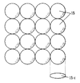
図2は任意の1つの対物レンズ15にかかわる画像入力のための基本ユニット(構成単位)を示す基本ユニット図、図3は多数の2次元配置の対物レンズ15を示すレンズ配列図である。図2、図3において、対物レンズ15、物体15a、画像導入部16、光検出部17は図1と同様のものなので、同一符号を付し、説明は省略する。図2の20はエリアセンサ、図3の15cは側面から見た対物レンズである。
【0027】
図2の基本ユニット、図3の多数の2次元対物レンズ15から成る対物レンズ群について、その構造、動作等を説明する。図2において、対物レンズ15の光軸は画像入力装置の凹面画像導入部16の接平面に垂直に取り付けられており、入射した光束は対物レンズ15それぞれの収斂作用を受け、光検出部17に結像される。この光検出部17は、図2に升目で示すような2次元の複数の光感受部(受光部)をもつエリアセンサ20から成り、複数の受光部に画像情報を取り込む。また、エリアセンサ20の領域幅と焦点距離とで規定されるところの画角による画像取込み範囲は、前述したように、隣接するエリアセンサと接触し、しかも重ならないようになっている。対物レンズ15は、図3に示すように、それぞれに有効口径を接触させながら配置されており、紙面の都合上平面ではあるが、凹曲面に沿った形で配置されてなるものである。図1、図2に示すように、エリアセンサ20は互いに離散して配置されている。これは、凹面の接平面に対物レンズ15の光軸が略直角となるように規定されていて物体15a側からみて対物レンズから離れるほどエリアが発散していくことと、画角を絞り込んでいることにより対物レンズ径と比べエリアセンサ20の寸法がかなり小さくなっていることによる。このような構造をとることによって、互いに隣接するエリアセンサに隣の対物レンズから光が漏れ込む影響を緩和することができる。
【0028】
図1の凹面状とは逆の凸面状の曲面も考えられるが、凸面による対物レンズ15群の配置ではエリアセンサ20の離散間隔が逆に狭くなって、隣接する対物レンズからの漏れ込みによるゴーストの発生などの悪影響を無視できなくなる可能性がある。また、図2において、対物レンズ15はその焦点距離がエリアセンサ20までの距離とほぼ一致するように規定された曲率をもつ凸レンズで形成されており、前述のように、その光軸はエリアセンサ20の中心と一致するように配置されている。
【0029】
図4は、多数のエリアセンサ20から成るエリアセンサ群を含む光検出面(凹面)を平面的に示す光検出面平面図である。21は光感受素子(受光部)であり、エリアセンサ20は多数の光感受素子21から成る。前述したように、1つの対物レンズ15に対しては1つのエリアセンサ20が対応しており、エリアセンサ20は内部に多数の光感受素子21つまり画素を持ち、対物レンズ15からの結像光を部分画像として捕らえる。この結像光はエリアセンサ20内のみに到達するだけでなく、周縁部にも影響を及ぼす。このためエリアセンサ20が互いに近接すると、前述のように、隣接する対物レンズからの漏れ込み光の影響を受け、画像のコントラストが低下したり、ゴーストの発生を起こしたりする。また、エリアセンサ20の画素数を増やすことによって対物レンズ15の数を減らすことができ、さらに、エリアセンサ20の画素数を増やすと対物レンズ15の口径が大きくなることから明るさを増大させることができるが、そうすると単レンズ画像入力装置の構造形態に近付くため厚み方向の増大を招いてしまう。また、むやみに対物レンズ15とこれに対応するエリアセンサ20とから成る基本ユニットの数を増大して厚みを縮小させても、対物レンズ15群を形成する凹面の厚みを減らすことはできないため得策とは言えない。また、明るさを確保できないため画像が暗くなってしまう。分解能は画角と総光感受素子数とで決まってくるため影響は少ないが、画像が暗くなってコントラストが低下する悪影響の方は分解能の場合よりも遙かに大きいと言える。
【0030】
それぞれのエリアセンサ20へ結像する画像は対物レンズ15の対向する領域をとらえる画像としてはそれぞれ独立したエリアごとに反転しているため、そのまま重ね合わせても求める画像は得られない。しかしながら、この得られたそれぞれの画像情報に対して信号処理を適切に行うことによって、求める総合画像を構成することができる。また、エリアセンサ20の配置されている曲面は対物レンズ15群を構成する凹面と曲率中心を同じくする凹面となるが、図4では平面として表した。
【0031】
図5は最終的に合成された合成画像を示す画面図である。図5において、大きな区切り線Lで区分けされた1つ1つの領域が1つの対物レンズによって得られた小領域部分画像で、この部分画像が組み合わされて合成画像として構成されている。この区切り線Lは説明のため分かりやすくした模式的なもので、実際にはほとんど目立たないようにすることができる。また、図4に示したエリアセンサ20ごとの反転も修正され、それぞれが正像へと揃えられている。これはソフトウェア的画像処理によって行われているものであるが、ソフトウェア的画像処理の技術は本発明とは直接は関係なく、本実施の形態では説明しない。
【0032】
なお、本実施の形態では対物レンズ15の配置を凹面配置としたが、本発明はこれに限定されず、たとえば放物線の回転体である放物面とすることもできる。また、対物レンズ15は凸レンズとしたが、バイナリーレンズ、屈折率が分布したレンズなどを用いることができ、本実施の形態に限定されるものではない。さらに、その構造も、本実施の形態で示したように凹面基板と一体に形成されているものや、レンズ部分を凹面基板とは別に形成して張り合わせる構造など、適宜採用することができる。さらに、視野制御部19の形状については何ら説明しなかったが、楕円形、矩形等のように効率的に視野制限できるものであれば良い。
【0033】
以上のように本実施の形態によれば、多数の画素から成るエリアセンサ20を採用して単眼的特徴を保持すると共に部分画像を合成して合成画像を得る複眼構造の画像入力装置とすることにより、画像取込み方向を薄型として、対物レンズ15を明るいレンズとすることができ、また、対物レンズ15群から成る曲面を凹面とすることによって対物レンズ15の多数配置が可能となり、さらに、空間的に視野がクロスするクロス部18に視野制御部19を設けることによりエリアセンサ20へ不要光が入射することによるコントラストの低下、ゴーストやフレアの発生を防止することができる。
【0034】
(実施の形態2)
図6は、本発明の実施の形態2による画像入力装置を示す構成図であり、画像導入部が平面状で、対物レンズとしてマイクロフレネルレンズを使用した場合を示す。図6において、22はマイクロフレネルレンズである対物レンズ、22aは被写体としての物体、22bは視野絞り(開口絞り)、23はエリアセンサである。図6の画像入力装置は、対物レンズ22群による画像導入部と、対物レンズ22群に対応するエリアセンサ23群とから成るハイブリッド構造の複眼の画像入力装置である。画像導入部は平面状であり、それぞれの画角の中心方向に対して中心部を除いて直角となっていない。また、各エリアセンサ23も平面状に設置されており、全体として薄型化が実現されている。
【0035】
図7は図6の対物レンズ22の配列を示す平面図、図8はエリアセンサの配列を示す平面図である。図7、図8において、対物レンズ22、エリアセンサ23は図6と同様のものなので、同一符号を付し、説明は省略する。24はエリアセンサ23を構成する光感受素子である。図7と図8との比較から分かるように、対物レンズ22の配列ピッチの間隔よりもエリアセンサ23の配列ピッチの間隔が大きく、このような配列ピッチとすることによって、それぞれの対物レンズ22が担う画角をうまく分割することができる。仮に対物レンズ22とエリアセンサ23との配列ピッチが等しければ、対物レンズ22の画角は重なってしまい、合成画像を取り出すことができなくなる。しかしながら、物体22aまでの距離が対物レンズ22の焦点距離近傍の場合は、図8のような配列ピッチとなる必要はないが、このような場合は特殊な場合であり、汎用的な使用を目的とした画像入力装置においては図8のような配列ピッチとして、無限遠の距離で画角、視野が重ならないようにする必要がある。また、対物レンズ22は平面状に配列されたレンズであるため、角方向から光線が入射し、対物レンズ22とそれに対応するエリアセンサ23とで規定される画角からのみの入射光線を期待することができない。このため、実施の形態1と同様、迷光、不要光除去のために用いられた視野絞り22bを用いることにより、より効果的に結像の品質の向上を図ることができる。
【0036】
以上のように本実施の形態によれば、平面状に配列された対物レンズ22とその対物レンズに対応するエリアセンサ23とを設けたことにより、対物レンズを凹曲面状に配列した場合よりも更に薄型にすることが可能となる。
【0037】
【発明の効果】
以上のように本発明の画像入力装置によれば、多数の対物レンズと多数の光電変換部とにより複眼状態となすことができるので、装置の薄型化を図ることができ、また、視野制限部により視野を制限することができるので、不要な光を入射を防止できるという有利な効果が得られる。
【0038】
また、曲面は凹面であることにより、対物レンズの光軸を導入しようとする画角の中心部に向けることができ、また空間的に視野が集中する部分を生じさせることができるので、視野が集中する部分に開口絞りを設けることができ、開口絞りにより迷光、不要な光が隣接する対物レンズから漏れることを防止できるという有利な効果が得られる。
【0039】
さらに、対物レンズはその光軸が曲面の接平面に垂直であることにより、結像の収差を小さく押さえることができるので、入力画像の品質の低下を防止することができるという有利な効果が得られる。
【0040】
さらに、光電変換部は2次元の受光部を複数有することにより、受光部を増やす、つまり画素数を増やすことによって分解能を向上でき、単純な複眼構造と比較して1画素に対する対物レンズの有効径を大きくすることができ、明るい画像を得ることができるという有利な効果が得られる。
【0041】
さらに、画像合成部は画像信号の合成を電気的処理によって行うことにより、像の反転や補正などの処理を行うことができるという有利な効果が得られる。
【0042】
さらに、視野制限部は楕円形または矩形の開口絞りであることにより、視野以外からの入射光を効率良く制限することができるので、ゴーストやコントラストの低下を抑制することができるという有利な効果が得られる。
【図面の簡単な説明】
【図1】本発明の実施の形態1による画像入力装置を示す構成図
【図2】任意の1つの対物レンズにかかわる画像入力のための基本ユニットを示す基本ユニット図
【図3】多数の2次元配置の対物レンズを示すレンズ配列図
【図4】多数のエリアセンサから成るエリアセンサ群を含む光検出面(凹面)を平面的に示す光検出面平面図
【図5】最終的に合成された合成画像を示す画面図
【図6】本発明の実施の形態2による画像入力装置を示す構成図
【図7】図6の対物レンズの配列を示す平面図
【図8】エリアセンサの配列を示す平面図
【図9】極めて一般的な従来の画像入力装置を示す構成図
【図10】従来の画像入力装置の他の例を示す構成図
【図11】複眼による画像入力装置を説明するための構成図
【図12】複眼による画像入力装置を説明するための構成図
【符号の説明】
15、22 対物レンズ
15a、22a 物体
16 画像導入部
17 光検出部(光電変換部)
18 クロス部
19 視野制限部
19´ 開口絞り部
20、23 エリアセンサ
21、24 光感受素子(受光部)
22b 視野絞り[0001]
BACKGROUND OF THE INVENTION
The present invention relates to an image input apparatus that forms an image with a plurality of objective lenses, that is, compound eyes.
[0002]
[Prior art]
In recent years, with the development of information transmission media, large-capacity and high-speed information can be easily used. In addition, most of the transmitted information has been voice or text data in the past, but in recent years, the proportion of image data such as still images and moving images has increased remarkably. In addition, information processing devices are increasingly required to be personal use and small and light, as represented by notebook computers and mobile phones. Therefore, it is expected that a compact image input device that can easily capture and process images at a personal level will be increasingly demanded in the future.
[0003]
FIG. 9 is a block diagram showing a very general conventional image input apparatus. In FIG. 9, 1 is an objective lens, 1a is an object as a subject, 1b is a field stop (aperture stop) for reducing the field of view, 2 is a CCD area sensor as a two-dimensional photoelectric conversion element, and 4 is shown in plan view. The inverted
[0004]
The operation and effect of the image input apparatus configured as described above will be described. The light beam taken into the
[0005]
FIG. 10 is a block diagram showing another example of a conventional image input apparatus. The image input device shown in FIG. 10 is an example of a proximity image input device, generally called a scanner, and used as a planar image input device. In FIG. 10, 5 is a signal processing unit that corrects an electrical signal, 5 a is a monitor unit for monitoring an image signal output from the
[0006]
The arrangement, operation, effects, etc. of the image input apparatus of FIG. 10 will be described. In FIG. 10, a light source unit 6 and a
[0007]
The image input apparatus shown in FIG. 10 is mainly used in an image input apparatus for inputting an image to a computer, an image copying apparatus, an image telegraph apparatus, and the like, and has a scanning mechanism 9 including an input screen sending section and an encoder section. Thus, a two-dimensional image can be captured by a one-
[0008]
In recent years, as a smaller and thinner image input device, an image input device using a compound eye as seen in the eyes of insects, crustaceans and the like has been attracting attention. A compound eye is different from a monocular such as a human being or a bird, that is, a single condensing lens that forms all images in the field of view. It consists of a light receiving unit that constructs information as a map by comprehensively recognizing the output images of each light receiving unit, and has a limited resolution, but does not require a focus adjustment mechanism, etc. Therefore, it is often found in relatively inferior animals such as insects and crustaceans. Further, since one pixel is captured by one lens and one detector, the resolution of the image increases as the minimum unit configuration increases. Furthermore, image input with a compound eye generally requires an imaging distance of several centimeters or more for the imaging action of the previous monocular, and several tens of centimeters for a camera lens or the like, but this is achieved with a thickness of several millimeters inside or outside. be able to. By using this short imaging distance, the thickness of the image input device can be reduced to a considerable extent.
[0009]
FIG. 11 and FIG. 12 are configuration diagrams for explaining an image input apparatus using compound eyes. In FIGS. 11 and 12, 10 is an objective lens, 10a is an object as a subject, 11 is a light receiving unit, 12 is a convex curved surface, 12a is an object as a subject, 12b is a composite field angle indicating a field of view, and 12c is a composite angle. It is an image.
[0010]
FIG. 11 shows one pixel constituting a compound eye, that is, one unit configuration. An
[0011]
[Problems to be solved by the invention]
However, in the image input apparatus including the objective lens (monocular) 1 and the
[0012]
In addition, in the image input apparatus that inputs a planar image by the scanner shown in FIG. 10, it is relatively easy to reduce the thickness of the imaging lens in the optical axis direction or the method perpendicular to the captured image surface, but it is spatially separated. Therefore, it is difficult to project a portion or a three-dimensional object onto the
[0013]
Further, the compound-eye image input apparatus shown in FIGS. 11 and 12 can be realized in a small size, particularly in a thin shape, but since the effective aperture is small, the light intensity of the light incident on the
[0014]
In this image input device, it is desired that the resolution and brightness can be greatly improved in a compound eye and thin image input device.
[0015]
SUMMARY OF THE INVENTION An object of the present invention is to provide a compound eye and thin image input device capable of greatly improving resolution and brightness.
[0016]
[Means for Solving the Problems]
In order to solve this problem, an image input device according to the present invention includes a large number of objective lenses distributed two-dimensionally on a curved surface, and a large number of objective lenses on an imaging plane on which a light beam introduced by the objective lens forms an image. A plurality of photoelectric conversion units arranged in a one-to-one correspondence, a field limiting unit for limiting each field of view of the optical system including the objective lens and the photoelectric conversion unit to a predetermined space, and a number of photoelectric conversions And an image synthesis unit that synthesizes image signals output from each of the units.
[0017]
Thereby, it is possible to obtain a thin image input device with compound eyes that can greatly improve resolution and brightness.
[0018]
DETAILED DESCRIPTION OF THE INVENTION
According to the first aspect of the present invention, a large number of objective lenses that are two-dimensionally distributed on a curved surface and a pair of objective lenses are formed on the imaging plane on which the light beam introduced by the objective lens forms an image. A plurality of photoelectric conversion units arranged corresponding to 1, a field-of-view restriction unit that limits the field of view of an optical system including the objective lens and the photoelectric conversion unit to a predetermined space, and each of a number of photoelectric conversion units An image synthesis unit that synthesizes the image signal output from the camera, and a compound eye state is formed by a large number of objective lenses and a large number of photoelectric conversion units. Has the effect of preventing incident light.
[0019]
The invention according to
[0020]
According to a third aspect of the present invention, in the first or second aspect of the present invention, the objective lens has an optical axis perpendicular to a tangential plane of the curved surface, and image forming aberration is suppressed. It has the action.
[0021]
The invention according to
[0022]
According to a fifth aspect of the present invention, in the first or second aspect of the invention, the image synthesizing unit synthesizes the image signal by electrical processing, and processing such as image inversion and correction is performed. Has the effect of being performed.
[0023]
The invention according to claim 6 is the invention according to
[0024]
Hereinafter, an embodiment of the present invention will be described with reference to FIG.
(Embodiment 1)
FIG. 1 is a block diagram showing an image input apparatus according to
[0025]
The function, operation, etc. of the image input apparatus configured as described above will be described. The light beam incident on the
[0026]
FIG. 2 is a basic unit diagram showing a basic unit (constituent unit) for inputting an image related to an arbitrary
[0027]
The structure, operation, etc. of the objective lens group including the basic unit of FIG. 2 and the many two-dimensional
[0028]
A convex curved surface opposite to the concave shape in FIG. 1 is also conceivable. However, in the arrangement of the
[0029]
FIG. 4 is a plan view of the light detection surface showing a light detection surface (concave surface) including an area sensor group composed of a large number of
[0030]
Since the image formed on each
[0031]
FIG. 5 is a screen view showing the synthesized image finally synthesized. In FIG. 5, each area divided by a large dividing line L is a small area partial image obtained by one objective lens, and the partial images are combined to form a composite image. The dividing line L is a schematic one that is easy to understand for the sake of explanation, and can be made almost inconspicuous in practice. Further, the inversion for each
[0032]
In the present embodiment, the
[0033]
As described above, according to the present embodiment, an
[0034]
(Embodiment 2)
FIG. 6 is a block diagram showing an image input apparatus according to
[0035]
7 is a plan view showing the arrangement of the
[0036]
As described above, according to the present embodiment, the
[0037]
【The invention's effect】
As described above, according to the image input device of the present invention, a compound eye state can be achieved by a large number of objective lenses and a large number of photoelectric conversion units. Thus, the field of view can be limited, so that an advantageous effect that unnecessary light can be prevented from entering can be obtained.
[0038]
In addition, since the curved surface is concave, the optical axis of the objective lens can be directed to the center of the field angle to be introduced, and a portion where the field of view is spatially concentrated can be generated. An aperture stop can be provided in the concentrated portion, and an advantageous effect that stray light and unnecessary light can be prevented from leaking from the adjacent objective lens by the aperture stop can be obtained.
[0039]
Further, since the objective lens has an optical axis perpendicular to the curved tangent plane, it can suppress the aberration of the image formation, and thus the advantageous effect that the deterioration of the quality of the input image can be prevented is obtained. It is done.
[0040]
Further, since the photoelectric conversion unit has a plurality of two-dimensional light receiving units, the resolution can be improved by increasing the number of light receiving units, that is, by increasing the number of pixels, and the effective diameter of the objective lens for one pixel as compared with a simple compound eye structure. The advantageous effect that a bright image can be obtained can be obtained.
[0041]
Furthermore, an advantageous effect that the image synthesis unit can perform processing such as image inversion and correction by synthesizing image signals by electrical processing.
[0042]
Furthermore, since the field limiting unit is an elliptical or rectangular aperture stop, it is possible to efficiently limit incident light from other than the field of view, so that an advantageous effect that ghost and contrast reduction can be suppressed. can get.
[Brief description of the drawings]
FIG. 1 is a configuration diagram illustrating an image input apparatus according to a first embodiment of the invention.
FIG. 2 is a basic unit diagram showing a basic unit for image input related to an arbitrary objective lens.
FIG. 3 is a lens arrangement diagram showing a number of two-dimensionally arranged objective lenses.
FIG. 4 is a plan view of a light detection surface showing in plan a light detection surface (concave surface) including an area sensor group composed of a large number of area sensors.
FIG. 5 is a screen diagram showing a synthesized image finally synthesized.
FIG. 6 is a block diagram showing an image input apparatus according to a second embodiment of the present invention.
7 is a plan view showing the arrangement of the objective lenses of FIG. 6;
FIG. 8 is a plan view showing an array of area sensors.
FIG. 9 is a block diagram showing a very general conventional image input device.
FIG. 10 is a configuration diagram illustrating another example of a conventional image input apparatus.
FIG. 11 is a configuration diagram for explaining an image input apparatus using compound eyes.
FIG. 12 is a configuration diagram for explaining an image input apparatus using compound eyes.
[Explanation of symbols]
15, 22 Objective lens
15a, 22a Object
16 Image introduction part
17 Photodetector (photoelectric converter)
18 Cross section
19 Field of view restriction
19 'aperture stop
20, 23 Area sensor
21, 24 Photosensitive element (light receiving part)
22b Field stop
Claims (6)
Priority Applications (1)
| Application Number | Priority Date | Filing Date | Title |
|---|---|---|---|
| JP26039296A JP3622367B2 (en) | 1996-10-01 | 1996-10-01 | Image input device |
Applications Claiming Priority (1)
| Application Number | Priority Date | Filing Date | Title |
|---|---|---|---|
| JP26039296A JP3622367B2 (en) | 1996-10-01 | 1996-10-01 | Image input device |
Publications (2)
| Publication Number | Publication Date |
|---|---|
| JPH10107975A JPH10107975A (en) | 1998-04-24 |
| JP3622367B2 true JP3622367B2 (en) | 2005-02-23 |
Family
ID=17347291
Family Applications (1)
| Application Number | Title | Priority Date | Filing Date |
|---|---|---|---|
| JP26039296A Expired - Fee Related JP3622367B2 (en) | 1996-10-01 | 1996-10-01 | Image input device |
Country Status (1)
| Country | Link |
|---|---|
| JP (1) | JP3622367B2 (en) |
Families Citing this family (7)
| Publication number | Priority date | Publication date | Assignee | Title |
|---|---|---|---|---|
| JP2000075357A (en) | 1998-08-28 | 2000-03-14 | Minolta Co Ltd | Image pickup unit |
| JP3821614B2 (en) | 1999-08-20 | 2006-09-13 | 独立行政法人科学技術振興機構 | Image input device |
| FR2861187B1 (en) * | 2003-10-21 | 2006-01-20 | Atmel Grenoble Sa | SHIFTING DEVICE WITH REDUCED SIZE |
| US7244925B2 (en) * | 2005-03-21 | 2007-07-17 | Avago Technologies Ecbu Ip (Singapore) Pte. Ltd | Compact and low profile optical navigation device |
| KR101410002B1 (en) | 2007-11-19 | 2014-06-20 | 삼성전자주식회사 | Image sensing apparatus with artificial ommatidia and Manufacturing method for artificial ommatidia unit |
| CN112866512B (en) * | 2019-11-26 | 2022-03-22 | 中国科学院上海微系统与信息技术研究所 | Compound eye imaging device and compound eye system |
| CN117233874B (en) * | 2023-11-16 | 2024-02-09 | 西安信飞特信息科技有限公司 | Image acquisition device and image acquisition equipment |
-
1996
- 1996-10-01 JP JP26039296A patent/JP3622367B2/en not_active Expired - Fee Related
Also Published As
| Publication number | Publication date |
|---|---|
| JPH10107975A (en) | 1998-04-24 |
Similar Documents
| Publication | Publication Date | Title |
|---|---|---|
| US11962906B2 (en) | Image processing systems for correcting processed images using image sensors | |
| CN105549305B (en) | Portable electronic equipment, camera shooting structure therein and method for acquiring image | |
| CN105611124B (en) | Imaging sensor, imaging method, imaging device and terminal | |
| US20120140097A1 (en) | Method and apparatus for image capturing capable of effectively reproducing quality image and electronic apparatus using the same | |
| US20130278802A1 (en) | Exposure timing manipulation in a multi-lens camera | |
| US20140139623A1 (en) | Panoramic multi-scale imager and method therefor | |
| US11659289B2 (en) | Imaging apparatus and method, and image processing apparatus and method | |
| US8264590B2 (en) | Imaging apparatus and method | |
| US11460666B2 (en) | Imaging apparatus and method, and image processing apparatus and method | |
| US11917298B2 (en) | Electronic device | |
| JP3622367B2 (en) | Image input device | |
| US7639293B2 (en) | Imaging apparatus and imaging method | |
| US12035058B2 (en) | Electronic equipment | |
| US20220343471A1 (en) | Electronic apparatus | |
| CN105093803B (en) | Panoramic imaging system | |
| WO2023090191A1 (en) | Imaging device | |
| WO2022163306A1 (en) | Imaging device and imaging method | |
| CN113810578B (en) | Under-screen camera module and display device | |
| US10498938B2 (en) | Imaging camera | |
| US8982270B2 (en) | Deformable focal plane array | |
| JP2005031460A (en) | Compound eye optical system | |
| JP2004309568A (en) | Omnidirectional photographing device | |
| CN112630932A (en) | Moire pattern imaging device | |
| JP2005260526A (en) | Imaging apparatus | |
| JP2022188066A5 (en) | Imaging element and imaging device |
Legal Events
| Date | Code | Title | Description |
|---|---|---|---|
| A977 | Report on retrieval |
Free format text: JAPANESE INTERMEDIATE CODE: A971007 Effective date: 20041012 |
|
| TRDD | Decision of grant or rejection written | ||
| A01 | Written decision to grant a patent or to grant a registration (utility model) |
Free format text: JAPANESE INTERMEDIATE CODE: A01 Effective date: 20041102 |
|
| A61 | First payment of annual fees (during grant procedure) |
Free format text: JAPANESE INTERMEDIATE CODE: A61 Effective date: 20041115 |
|
| FPAY | Renewal fee payment (event date is renewal date of database) |
Free format text: PAYMENT UNTIL: 20071203 Year of fee payment: 3 |
|
| FPAY | Renewal fee payment (event date is renewal date of database) |
Free format text: PAYMENT UNTIL: 20081203 Year of fee payment: 4 |
|
| FPAY | Renewal fee payment (event date is renewal date of database) |
Free format text: PAYMENT UNTIL: 20091203 Year of fee payment: 5 |
|
| FPAY | Renewal fee payment (event date is renewal date of database) |
Free format text: PAYMENT UNTIL: 20091203 Year of fee payment: 5 |
|
| FPAY | Renewal fee payment (event date is renewal date of database) |
Free format text: PAYMENT UNTIL: 20101203 Year of fee payment: 6 |
|
| FPAY | Renewal fee payment (event date is renewal date of database) |
Free format text: PAYMENT UNTIL: 20101203 Year of fee payment: 6 |
|
| FPAY | Renewal fee payment (event date is renewal date of database) |
Free format text: PAYMENT UNTIL: 20111203 Year of fee payment: 7 |
|
| FPAY | Renewal fee payment (event date is renewal date of database) |
Free format text: PAYMENT UNTIL: 20111203 Year of fee payment: 7 |
|
| FPAY | Renewal fee payment (event date is renewal date of database) |
Free format text: PAYMENT UNTIL: 20121203 Year of fee payment: 8 |
|
| LAPS | Cancellation because of no payment of annual fees |