JP2004032172A - Fly-eye imaging device and equipment comprising the same - Google Patents
Fly-eye imaging device and equipment comprising the same Download PDFInfo
- Publication number
- JP2004032172A JP2004032172A JP2002182934A JP2002182934A JP2004032172A JP 2004032172 A JP2004032172 A JP 2004032172A JP 2002182934 A JP2002182934 A JP 2002182934A JP 2002182934 A JP2002182934 A JP 2002182934A JP 2004032172 A JP2004032172 A JP 2004032172A
- Authority
- JP
- Japan
- Prior art keywords
- image
- subject
- compound
- imaging
- images
- Prior art date
- Legal status (The legal status is an assumption and is not a legal conclusion. Google has not performed a legal analysis and makes no representation as to the accuracy of the status listed.)
- Withdrawn
Links
Images


Classifications
-
- H—ELECTRICITY
- H04—ELECTRIC COMMUNICATION TECHNIQUE
- H04N—PICTORIAL COMMUNICATION, e.g. TELEVISION
- H04N25/00—Circuitry of solid-state image sensors [SSIS]; Control thereof
- H04N25/40—Extracting pixel data from image sensors by controlling scanning circuits, e.g. by modifying the number of pixels sampled or to be sampled
- H04N25/41—Extracting pixel data from a plurality of image sensors simultaneously picking up an image, e.g. for increasing the field of view by combining the outputs of a plurality of sensors
Abstract
Description
【0001】
【発明の属する技術分野】
本発明は、複数のレンズ部を略並列に配置した複眼光学素子により被写体像を撮像する複眼撮像装置に関するものである。
【0002】
【従来の技術】
上記のような複眼撮像装置において、複数のレンズ部のそれぞれの光軸が互いに傾き、それぞれのレンズ部を通して被写体の互いに異なる領域の像(以下、被写体部分像という)を撮像することによって被写体全体の画像を得るものが従来提案されている。
【0003】
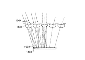
図12は、上記複眼撮像装置の断面を示す図である。図中、1001は複数の集光力を有するレンズ部を並列配置した複眼光学素子、1002はCCDやCMOSなどの光電変換素子からなる撮像素子、1003は撮像素子1002上に被写体からの光束を集光させるマイクロレンズ、1004は開口絞りである。
【0004】
図示しない被写体からの光束は、開口絞り1004および複眼光学素子1001に配置されたレンズ部を通過し、マイクロレンズ1003によって集光されて撮像素子1002上に結像する。結像した光束は、撮像素子1002によって被写体の反射率に応じた電気信号に変換され、この電気信号をアナログ/デジタル変換することによって被写体画像信号を得る。
【0005】
図13は、図12に示した複眼撮像素子1001の正面図である。前述したように、複眼光学素子1001はレンズ部1101が複数並列に配置されて構成されている。図12に示すように、それぞれのレンズ部1101の光軸は互いに傾き、異なる視野領域(撮影画面領域)を有している。
【0006】
なお、ここでいう光軸とは、開口絞り1004の開口の中心を通って個々のレンズ部1101に入射し、該個々のレンズ部に一対一に対応して形成された撮像領域の中心に到達する光線によって表される軸のことをいう。以下、本発明の実施形態の説明においても同様とする。
【0007】
図14は、図12に示した撮像素子1002の正面図である。撮像素子1002上には、それぞれ複数の光電変換素子(画素)からなる撮像領域1201が複数形成されており、個々の撮像領域1201は、個々のレンズ部1101に一対一に対応して被写体部分像が結像するように所定間隔を空けて配置されている。
【0008】
一方、図15には、略全面が撮像可能領域となっている撮像素子1002を示しており、個々のレンズ部1101により形成される被写体部分像が撮像素子1002上において互いに重ならないように、すなわち、図中に示した各矩形領域1301に結像する。
【0009】
【発明が解決しようとする課題】
しかしながら、図14で示したように、複眼光学素子の複数のレンズ部により形成される複数の被写体部分像は、撮像素子1002上の複数の撮像領域1201にてそれぞれ撮像されており、これら複数の被写体部分画像から1枚の被写体全体画像を得るためには、各撮像領域1201にて撮像された被写体部分画像の合成処理が必要である。
【0010】
また、図15に示すように、単一の撮像可能領域に各レンズ部に対応した撮像領域1301と非結像領域とが混在している場合に、1枚の被写体全体画像を得るためには、撮像領域1301の指定と各撮像領域1301により撮像された画像の合成処理とが不可欠である。
【0011】
さらに、複眼光学素子1001に設けられた複数のレンズ部はそれぞれ、個別の収差を有するため、隣り合う撮像領域1003による撮像画像を合成しただけでは繋ぎ部分が不連続となってしまう。したがって、その合成処理にはレンズ収差を補正した滑らかな合成を行うことが必要である。
【0012】
そこで、本発明は、複数の撮像領域で撮像された複数の被写体部分画像から連続した1枚の被写体全体画像を得ることができるようにした複眼撮像装置およびこれを備えた情報端末機器を提供することを目的としている。
【0013】
【課題を解決するための手段】
上記の目的を達成するために、本発明では、集光力を有する複数のレンズ部(例えば、光軸が互いに傾いている複数のレンズ部)を略並列に配置して構成される複眼光学素子と、上記複数のレンズ部のそれぞれによって形成される、被写体の複数領域の像(被写体部分像)を互いに異なる撮像領域で撮像する撮像素子とを有する複眼撮像装置において、上記複数の撮像領域のそれぞれによって(同時に)撮像された複数の画像(被写体部分画像)から被写体全体の画像を得るための合成処理を行う画像合成手段を設けている。
【0014】
これにより、複眼光学素子の各レンズ部を通して撮像した複数の被写体部分画像から、連続した1枚の合成画像(すなわち、被写体全体画像)を得ることが可能となる。
【0015】
具体的には、画像合成手段に、例えば、各撮像領域に形成される像の並び替えに相当する処理を行わせる。
【0016】
また、複数の撮像領域のそれぞれで撮像する被写体領域(被写体部分領域)に、相互に隣り合う被写体領域間において重複する部分を持たせ、画像合成手段に、上記重複する部分が一致するように合成処理を行わせるようにしてもよい。
【0017】
すなわち、複眼光学素子に配置されているレンズ部の光軸方向やレンズ間隔が一定であることを利用して予め大まかな隣り合う被写体領域間の対応する点(すなわち対応点)の位置関係が分かれば、対応点探索の範囲を極めて小さくすることが可能で、高速な対応点探索が可能となり、対応点を繋ぎ合わせることにより高精度な合成画像を得ることが可能となる。
【0018】
なお、撮像素子を光機能素子にすることで、エッジ抽出などの処理をオンチップ化されたマイクロプロセッサによって行なわせ、さらに高速な対応点探索が可能となる。
【0019】
さらに、画像合成手段に、各撮像領域で撮像された画像に対し、各レンズ部により生じた歪みの補正処理を行わせるようにしてもよい。これにより、歪みなく滑らかにつなぎ合わされた被写体全体画像を得ることが可能となる。
【0020】
そして、本発明の複眼撮像装置は、カード型カメラやノート型パーソナルコンピュータ等の各種機器に設けることができる。
【0021】
【発明の実施の形態】
(第1実施形態)
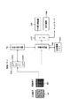
図1には、本発明の第1実施形態である複眼撮像装置の構成を表すブロック図である。
【0022】
図中、101は不図示の被写体からの光束に対して集光力を有する複数のレンズ部が略並列に配置されて構成される複眼光学素子である。102は複眼光学素子101によって結像された被写体像をアナログ電気信号に変換する光電変換素子を含む撮像素子であり、CCDやCMOSセンサなどから構成される。
【0023】
撮像素子102上には、複眼光学素子101の各レンズ部に1対1に対応するように撮像領域が配置されている。
【0024】
これら複眼光学素子101および撮像素子102を含む本実施形態の撮像光学系は、図12〜14にて説明した従来の複眼光学素子1001および撮像素子1002を含む撮像光学系と同様に構成されている。
【0025】
すなわち、不図示の被写体からの光束は、不図示の開口絞りおよび複眼光学素子101に配置されたレンズ部を通過し、不図示のマイクロレンズによって集光されて撮像素子102上に結像する。結像した光束は、撮像素子102によって被写体の反射率に応じた電気信号に変換され、その後、後述するように処理される。
【0026】
なお、撮像素子102として図15に示した全面が撮像可能領域である撮像素子を用いてもよい。
【0027】
103はA/D変換器であり、撮像素子102から出力されたアナログ信号をデジタル画像信号に変換する。104は画像メモリであり、デジタル信号に変換された各撮像領域で撮像された被写体部分画像を表す画像信号を一時的に記憶保持しておくものである。
【0028】
105は複眼光学素子101を構成する個々のレンズ部の収差によって各撮像領域での撮像画像に生じた歪みを補正するためのレンズ収差補正部である。
【0029】
106は画像メモリ104に記憶保持された各撮像領域で撮像された被写体部分画像を表す画像信号を1枚の被写体全体画像を表す画像信号に合成処理する合成処理部である。
【0030】
107は合成された画像信号を記録又は表示するための外部記憶装置108および表示装置109とのインターフェースである。
【0031】
次に、本実施形態の複眼撮像装置の動作について説明する。ここでは、複眼撮像装置による1回の撮影動作によって、連続した一画面をなす被写体全体画像を得る静止画撮影用の撮像装置として説明する。但し、1回の撮影動作によって時間的に連続したフレーム画像(すなわち動画)を撮像する動画撮影装置について、以下に説明する本発明の特徴とする処理動作を一定の速さで繰り返させるようにしてもよい。
【0032】
まず、撮影者が不図示の電源スイッチを投入すると、複眼光学素子101に配列された異なる視野領域(撮影画面領域)を持つレンズ部がそれぞれ被写体からの光束を撮像素子102上の対応する撮像領域に結像させる。
【0033】
撮像素子102上の各撮像領域からは、被写体光束による露光量に応じたアナログ電気信号が発生する。
【0034】
撮像素子102の各撮像領域から出力されたアナログ電気信号には、図示しないアナログ画像処理部でゲインアンプなどによる出力信号の増幅、サンプルホールドなどの処理が施され、AD変換器103によって被写体部分画像を表すデジタル画像信号に変換される。
【0035】
デジタル画像信号に変換された被写体部分画像は、一旦、画像メモリ104に記憶保持される。画像メモリ104では、撮像素子102上の撮像領域ごとにメモリ領域(アドレス)が区分されており、各メモリ領域1041、1042、…104n(n=1,2,3…)に識別子が付加されている。
【0036】
また、各メモリ領域1041、1042、…104nには、それぞれの撮像領域に対応するレンズ部も対応付けられており、対応するレンズ部の収差に関する情報が記憶保持されている。
【0037】
ここで、本実施形態の複眼撮像装置における固有の結像関係について図2を用いて説明する。
【0038】
図2(a)には本実施形態の複眼光学素子に相当する複眼レンズを用いた撮像装置、図2(b)には本実施形態との比較のために示した単レンズを用いた撮像装置を示している。
【0039】
これらの図中、201は被写体面の濃度分布を表しており、図2(a)および図2(b)に示す撮像光学系はいずれも、被写体濃度201に対応した濃度分布を有する被写体像を撮像素子204上に形成する。
【0040】
図2(a)において、複眼レンズ202は各レンズ部によって被写体を図中に矢印で示す3つの領域に分割し、それぞれの部分像(被写体像205)を撮像面204上に結像させる。この際、各レンズ部は各部分像を倒立像として撮像面204上に形成する。
【0041】
一方、図2(b)において、単レンズ203は、被写体全体の倒立像(被写体像206)を撮像面204上に形成する。
【0042】
この関係をさらにわかりやすくするため、図3(a),(b)を用いて、2次元平面被写体に対する複眼レンズと単レンズによる像形成を比較して説明する。
【0043】
図中、被写体201はどちらも平面上に描かれた「K」の文字である。図3(a)に示す単レンズ203は、被写体「K」全体を1つの視野領域とし、被写体「K」全体の倒立像(被写体像)206を撮像素子上に形成する。
【0044】
一方、図3(b)に示す、レンズ部を3行3列に配列した複眼レンズ202は、被写体201を図示のようなレンズ部に対応した9つの領域に分割し、それぞれの部分像の倒立像(被写体像)205を撮像素子上に形成する。
【0045】
図3(b)の複眼レンズ202による被写体像206は、図3(a)の単レンズ203による被写体像205と異なり、中心のレンズ部により形成される像の中心を軸とした点対称に配置されている。したがって、撮像素子102上に結像した複数の被写体部分像はそれらの合成時に被写体像206のように連続した1枚の被写体像となるように並べ替える必要がある。
【0046】
図4(a)は、前述した「K」の文字の被写体である。この被写体は、複眼光学素子101によって撮像素子102上に領域分割されて結像し、撮像素子102によって撮像される。
【0047】
図4(b)は、分割撮像された被写体を表す図であり、それぞれの分割画像(被写体部分画像)は画像メモリ104のメモリ領域1041,1042,…104nにそれぞれ記憶保存される。
【0048】
画像メモリ104に記憶された被写体部分画像に対しては、各レンズ部の収差補正が行われる。
【0049】
一般に、複数の画像から1枚の合成画像を作る場合、1台のカメラがパン・チルトして隣接する異なる視野領域を撮影するか、n台の同仕様のカメラが隣接する異なる視野領域を同一撮影条件で撮影するなどし、得られた複数の画像を合成する。
【0050】
このような場合、複数の画像間にはレンズの収差による歪みがあるが、画像中の同一画角領域では同じ収差補正式が適応できる。
【0051】
一方、本実施形態における複眼光学素子のレンズ部は個々に異なるレンズ特性を有し、収差もそれぞれ異なる。
【0052】
このため、レンズ収差補正部105では、画像メモリ104の各メモリ領域1041〜104nに記憶された各画像に対して個別に収差補正を行う。
【0053】
画像の収差補正に関しては様々な手法が提案されているが、特に画像合成で問題になるのは画像の歪曲であり、本実施形態でも、歪曲補正を行う。但し、より厳密にその他の収差補正も行なってもよい。
【0054】
歪曲補正に関しては多くの場合、座標変換によって補正することができ、予めレンズ設計値またはレンズ設計値を元に実験で修正を加えた座標変換式をレンズ部毎に作成しておく。レンズ収差補正部105では、各メモリ領域1041〜104nに記憶された画像ごとに、その画像に対応するレンズ部固有の座標変換式を適応して歪曲補正を行なう。
【0055】
レンズ収差補正部105から出力された画像データは、次に、画像合成部106に入力されて1枚の画像への合成処理が行われる。
【0056】
画像合成部106では、まず画像メモリ104に記憶された複数の画像から隣接して繋ぎ合わせる画像の対応を関係づける。すなわち、図4(b)で示したように、複眼光学素子101の個々のレンズ部によって撮像面上に結像された画像は、上述したように倒立像であり、かつ中心のレンズ部による画像の中心を軸とした点対称配置となっているため、そのまま隣合う画像を繋ぎ合わせても元の被写体を再現しない。
【0057】
このため、画像を繋ぎ合わせる前に並び変えに相当する処理を行ない、それぞれの配置関係を画像メモリ104又は不図示の別のメモリに記憶する。
【0058】
図5は、この並び替え処理を表す概念図であり、図5(a)に示すように、中央のレンズ部を中心とした点対称に配置された各画像を、前述した単レンズによる被写体像と同じ画像が得られるように並び変える。
【0059】
図5(a)に示した矢印は、各画像の並び替えの移動先を表し、中央のレンズ部を中心として点対称に並び替えることによって、図5(b)に示すような画像配列を得る。
【0060】
但し、実際に各画像を移動させて並び替えを行なうのではなく、例えば、画像メモリ104のメモリ領域1045に記憶された画像の右側にメモリ領域1044に記憶された画像を、左側にメモリ領域1046に記憶された画像などというように、合成時に繋ぎ合わせる画像の配置関係を記憶させておく。
【0061】
図5(c)には、メモリ領域1041〜1049に記憶された9つの画像のうちメモリ領域1041〜1048に記憶された画像とその上下左右に配置される画像との対応表であり、この表の配置関係が画像メモリ104又は不図示の別のメモリに記憶され、これを元に画像合成(並び替えに相当する処理)が行なわれる。なお、この配置関係は複眼光学素子101の設計段階で決まるものであり、本発明においてこの配置関係に限られるものではない。
【0062】
このようにして各画像の繋ぎ合わせ配置が確定すると、次に実際の繋ぎ合わせが行なわれる。画像の繋ぎ合わせについては様々な方式が提案されているが、ここではアフィン変換による画像の座標変換で合成を行なう方式について説明する。
【0063】
図6(a)は、画像メモリ104に記憶された各画像を表す(図中の符号1041〜1049は同符号が付されたメモリ領域に記憶された画像であることを示す)。
【0064】
画像メモリ104に記憶されたそれぞれの画像は、図中に矢印で示すようにxy座標系を有している。以下、この座標系を分割画像座標という。
【0065】
また、画像合成部106は、このとき合成画像を合成画像メモリに記憶させる。図1および図6(b)において、601は合成画像メモリを表す。合成画像メモリ601は、図6(b)中に矢印で示すようにXY座標系を有している。以下、この座標系を合成画像座標という。
【0066】
画像合成では、画像メモリ104のに記憶された被写体部分画像を隙間なく繋ぎ合わせて合成画像メモリ601に書き込み、1枚の連続した被写体全体画像である合成画像を作成する。以下、その方法について説明する。
【0067】
まず、合成画像メモリ601のほぼ中央の予め決められた位置を始点とし、複眼光学素子101に形成された複数のレンズ部のうち中央のレンズ部により形成され、対応する撮像領域で撮像された画像1045を合成画像メモリ601に書き込む(図6(c))。
【0068】
以下、この画像を元に周辺画像を配置していく。図6(d)は、画像1045の左隣に画像が繋ぎ合わされていることを表す図であり、画像1045の左隣は図5(c)の表より、画像1046が繋ぎ合わされる。 また、合成画像メモリ601への書き込みには、下記のアフィン変換式が適応される。
【0069】
【数1】

ここで、(x,y)は分割画像座標、(X,Y)は合成画像座標、a,b,c,dは変換パラメータでa,bが回転に関するパラメータ、c,dは平行移動に関するパラメータである。
【0071】
これら変換パラメータは、複眼光学素子101に形成されたレンズ部それぞれの光軸方向や配置間距離によって決まる値であり、レンズ部毎に予め決定されてメモリなどに記憶されているものとする。
【0072】
このように、合成画像メモリ601上において画像1045に画像1046が繋ぎ合わさると、画像1045を中心に順次周辺画像の合成が行なわれる。
【0073】
図6(e)は、画像1045を中心に上下左右に画像1042,1044,1046,1048が合成されている図、図6(f)は斜め方向に画像1041,1043,1047,1049が合成されて、最終的に3行×3列の9画像が合成されているところを表す。
【0074】
以上のように合成された画像(被写体全体画像)のデータは、以降、通常のデジタル撮像装置と同様に、様々な機能(編集機能やエッジ強調、色変換など)を有する不図示のデジタル画像処理部によって処理され、インターフェース107を介して磁気テープ、光磁気ディスクなどの外部記憶装置108に記録保持されたり、CRTや液晶ディスプレイなどの表示装置109に表示されたり、あるいはネットワーク伝送路によって遠隔地に伝送されたりする。
【0075】
このように、本実施形態によれば、複眼光学素子101の各レンズ部を通して撮像された複数の被写体部分画像から1枚の広視野領域の合成画像(被写体全体画像)を得ることができる。
【0076】
(第2実施形態)
図8には、本発明の第2実施形態である複眼撮像装置の構成を示している。図8において、第1実施形態と異なる点は、対応点検出部701が付加されている点と、画像合成部702が第1実施形態の画像合成部106とは機能的に異なる点であり、その他の構成については第1実施形態と同様であり、共通する構成要素には第1実施形態と同符号を付している。
【0077】
画像合成部702が第1実施形態の画像合成部106と機能的に相違する点は、第1実施形態においては画像メモリ104に記憶保持された各被写体部分画像を合成画像メモリに書き込む際の変換式に関し、予めそれぞれのレンズ部に対応した変換パラメータが決定されていたが、本実施形態では、より厳密な画像合成を行なうため、複眼光学素子101の各レンズ部の視野領域(つまりは撮像素子102の撮像領域によって撮像される被写体領域)を、隣り合う領域間で重複部分を有するように設定し、各レンズ部を通して各撮像領域で撮像された各画像の重複部分から被写体の同一部分(以下、この点を対応点という)を検出し、変換パラメータに修正を加える点である。
【0078】
以下、具体的に本実施形態の複眼撮像装置の動作について説明する。被写体が複眼光学素子101によって視野分割され、各被写体部分が撮像素子102の各撮像領域で撮像され、各画像がレンズ収差補正部105で収差補正されて画像メモリ104の各メモリ領域1041〜104nに記憶保持されるまでは第1実施形態と同様である。
【0079】
ただし、本実施形態では、撮像素子102における隣り合う撮像領域によって撮像される被写体領域(被写体部分像)の一部が互いに重複している。つまり、隣り合う撮像領域によって被写体の同一点がそれぞれ撮像される。
【0080】
図8(a)は、前述した被写体「K」を9個のレンズ部で互いに視野領域の一部が重複するように撮像していることを示す図である。図中、2つの異なる向きのハッチング領域が、隣り合う視野領域の一部Wが重複するように撮像する2つの撮影領域を示している。
【0081】
図8(b)には、「K」のうち図8(a)にハッチングして示した2つの撮像領域によって撮像された画像(被写体部分画像)を示している。このように撮像され、画像メモリ104に記憶保持された2つの画像内で、対応点検出部701によって変換パラメータ補正のために対応点が検出される。
【0082】
一般に、対応点の検出は、テンプレートマッチング法が使われ、本実施形態でもテンプレートマッチング法を用いる。
【0083】
但し、本実施形態の複眼撮像装置は、それぞれのレンズは複眼光学素子に固定的に配置されている。また、第1実施形態で述べたように、各分割画像(被写体部分画像)の座標系から合成画像座標系への変換パラメータが予め既知であることから、複眼光学素子101におけるレンズ間座標変換式は、合成画像座標系を介して一義的に決まる。
【0084】
よって、一般のテンプレートマッチング法に比べて格段に対応点のサーチ領域を狭めることが可能である。
【0085】
図8(b)において、801はテンプレートである。テンプレートの選び方は、テンプレート801内でエッジ部のコーナーなど、形状的に特徴のある被写体部分や色や明るさなどテクスチャーに特徴のある被写体部分が望ましい。
【0086】
また、分割画像座標系から合成画像座標系への変換式の他に、異なるレンズ部の分割画像座標系へ変換式は予め決定しておく。
【0087】
テンプレート801の中心座標から隣接する画像の位置座標が求まると、この位置座標を中心とした予め決められた幅の狭領域をサーチ領域とする。
【0088】
図8(b)に示す802は、隣接画像のサーチ領域を表す。テンプレート801は、サーチ領域内を順次移動し、テンプレート領域内の対応する画素と差分の絶対値をとり、テンプレート領域全画素についての総和を計算し、総和が最小となる点を対応点とする。
【0089】
このような対応点を少なくとも4つ選び、▲1▼式に代入して作成された連立方程式を解くことにより、分割画像間を変換するアフィン変換のパラメータa,b,c,dが決定される。なお、対応点を4個以上求めて最小二乗法によりアフィン変換のパラメータa,b,c,dを求めてもよい。
【0090】
以上のようにして、対応点検出部701では各分割画像間の重複した被写体像の対応点を検出するとともに、各分割画像間の変換パラメータを決定する。次に、画像合成部702では、各分割画像間の変換パラメータを用いて、例えば複眼光学素子101に形成された中央のレンズ部により形成される画像を基準として、隣接する画像を分割画像間変換パラメータを用いて順次、合成画像メモリ601上に繋ぎ合わせながら書き込んでいく。
【0091】
こうして最終的に全ての分割画像が繋ぎ合わされると、第1実施形態にて説明したように、合成画像のデータをインターフェース107を介して外部記憶装置108や表示装置109へと出力する。
【0092】
このように、本実施形態によれば、複眼光学素子101の各レンズ部の光軸方向やレンズ間隔が一定であることを利用して、予め大まかな対応点の位置関係を想定して対応点探索のサーチ範囲を極めて小さくすることができるため、高速な対応点探索が可能となり、対応点を繋ぎ合わせることにより高精度な合成画像(被写体全体画像)を得ることができる。
(第3実施形態)
図9には、本発明の第3実施形態である複眼撮像装置の構成を示している。図9において、第1実施形態および第2実施形態と異なる点は、撮像素子901がその全面が撮像可能領域となっており、撮像画像の信号処理機能をオンチップ化した光機能素子(ビジョンセンサやビジョンチップとも呼ばれる)であること、およびA/D変換機能およびレンズ収差補正機能が撮像素子901にオンチップ化されている点である。なお、第1実施形態と共通する構成要素には、第1実施形態と同符号を付している。
【0093】
以下、具体的に本実施形態の複眼撮像装置の動作について説明する。被写体は複眼光学素子101によって視野分割される。各被写体部分像は、撮像素子901、すなわちCMOSセンサにより構成される撮像可能領域が全面に配置され、後述する画像処理部がオンチップ化された光機能素子によって撮像される。
【0094】
撮影画像は、オンチップ化された図示しないマイクロプロセッサのエッジ抽出フィルターによってそのエッジ部が検出され、エッジ信号はマイクロプロセッサにオンチップ化されたA/D変換機能でデジタル変換される。
【0095】
一方、CMOSセンサの任意領域読み取り機能から、撮像面上の予め調べられた各レンズ部に対応する撮像領域のアドレスを読み出し開始位置として、複数のエッジ画像(分割画像)が画像メモリ104に記憶保持される。
【0096】
このときCMOSセンサの読み出し位置はレンズの収差補正関数によって補正されたアドレスを示す。画像メモリ104に記憶保持されたエッジ画像については、対応点検出部701によって第2実施形態にて説明した対応点がテンプレートマッチング法などによって検出され、画像間変換パラメータが決定される。パラメータの決定方法については第2実施形態と同様である。
【0097】
変換パラメータが決定されると、画像合成部702は、CMOSセンサ上の隣接する撮像領域に対応するレンズ部の収差補正関数によって補正されたアドレスを順次指定して、複数の分割画像を合成し、順次、画像メモリ601上に繋ぎ合わせながら書き込んでいく。
【0098】
こうして最終的に全ての分割画像が繋ぎ合わされると、第1実施形態にて説明したように、合成画像のデータをインターフェース107を介して外部記憶装置108や表示装置109へと出力する。
【0099】
このように、本実施形態によれば、撮像素子901を光機能素子にすることで、エッジ抽出など演算負荷の重い処理をオンチップ化されたマイクロプロセッサによって行なわせることができ、さらに高速な対応点探索が可能となる。
【0100】
(第4実施形態)
図10には、上記第1〜第3実施形態にて説明した複眼撮像装置としてのカード型カメラを示している。このカメラ200は、カード型のカメラ本体205に、開口絞り付きの複眼光学素子および撮像素子等からなる複眼撮像光学系201と、ファインダー窓202と、シャッターボタン203と、フラッシュ204とを設けて構成されている。
【0101】
複眼撮像系201により撮影された画像は、上記第1〜第3実施形態にて説明したように合成処理され、カメラ本体205内の合成画像メモリに記憶される。また、この合成画像のデータは、インターフェースを介してコンピュータのハードディスクに記憶保存されたり、コンピュータ画面上に表示されたり、プリントアウトされたりする。
【0102】
(第5実施形態)
図11には、上記第1〜第3実施形態にて説明した複眼撮像装置を備えたノート型若しくは携帯型コンピュータ(電子機器)を示している。
【0103】
このコンピュータ300の画面部301の上部には、上記第1から第3実施形態にて説明した複眼撮像装置303が回転可能に保持されている。そして、使用者のコンピュータ操作に応じて複眼撮像装置303を動作させることにより、使用者や他の被写体の静止画又は動画を撮像することができる。
【0104】
【発明の効果】
以上説明したように、本発明によれば、複眼光学素子の各レンズ部を通して撮像した複数の被写体部分画像から、連続した1枚の合成画像である被写体全体画像を得ることができる。
【0105】
また、各被写体部分画像に対し、各レンズ部により生じた歪みの補正処理を行わせるようにすれば、歪みなく滑らかにつなぎ合わされた被写体全体画像を得ることができる。
【図面の簡単な説明】
【図1】本発明の第1実施形態である複眼撮像装置の構成を表すブロック図である。
【図2】(a)は上記第1実施形態の複眼撮像装置の断面図、(b)は単レンズを用いた撮像装置の断面図である。
【図3】(a)は単レンズを用いた撮像装置での被写体像の結像関係を説明する図、(b)は複眼レンズを用いた撮像装置での被写体像の結像関係を説明する図である。
【図4】(a)は上記第1実施形態にて用いられる複眼光学素子による被写体分割の様子を示す図、(b)は撮像面での分割像を表す図である。
【図5】(a)、(b)は上記第1実施形態の複眼撮像装置における合成処理を説明する図、(c)は各分割画像の並べ替え後の配置関係を示す表である。
【図6】(a)〜(f)は上記第1実施形態の複眼撮像装置における画像合成の手順を示す図である。
【図7】本発明の第2実施形態である複眼撮像装置の構成を表すブロック図である。
【図8】(a)は上記第2実施形態の複眼撮像装置において重複部分を有する被写体領域を撮像する撮像領域を示す図、(b)は重複部分を有する画像から対応点を探索する際のテンプレートと探索範囲を示す図である。
【図9】本発明の第3実施形態である複眼撮像装置の構成を表すブロック図である。
【図10】本発明の第4実施形態であるカード型カメラを示す斜視図である。
【図11】本発明の第5実施形態である複眼撮像装置を備えたノート型パソコンを示す斜視図である。
【図12】従来の複眼撮像装置を示す断面図である。
【図13】従来の複眼撮像素子を示す正面図である。
【図14】従来の撮像素子を示す正面図である。
【図15】従来の撮像素子を示す正面図である。
【符号の説明】
101 複眼光学素子
102 撮像素子
103 A/D変換器
104 画像メモリ
105 レンズ収差補正部
106 画像合成部
107 インターフェース
108 外部記憶装置
109 表示装置
201 被写体
202 複眼レンズ
203 単レンズ
204 撮像面
205 被写体像
206 被写体像
601 合成画像メモリ
701 対応点検出部
702 画像合成部
801 テンプレート
802 探索領域
901 撮像素子(光機能素子)
1001 複眼光学素子
1002 撮像素子
1003 マイクロレンズ
1004 開口絞り
1101 レンズ部
1201 撮像領域
1301 撮像領域[0001]
TECHNICAL FIELD OF THE INVENTION
The present invention relates to a compound-eye imaging device that captures a subject image using a compound-eye optical element in which a plurality of lens units are arranged substantially in parallel.
[0002]
[Prior art]
In the compound-eye imaging device as described above, the optical axes of the plurality of lens units are inclined with respect to each other, and images of different regions of the subject (hereinafter, referred to as subject partial images) are taken through the respective lens units, thereby capturing the entire subject. A device for obtaining an image has been conventionally proposed.
[0003]
FIG. 12 is a diagram showing a cross section of the compound eye imaging apparatus. In the figure,
[0004]
A luminous flux from a subject (not shown) passes through an
[0005]
FIG. 13 is a front view of the compound
[0006]
Note that the optical axis referred to here is incident on each lens unit 1101 through the center of the aperture of the
[0007]
FIG. 14 is a front view of the
[0008]
On the other hand, FIG. 15 illustrates an
[0009]
[Problems to be solved by the invention]
However, as illustrated in FIG. 14, a plurality of subject partial images formed by a plurality of lens units of the compound eye optical element are captured in a plurality of
[0010]
Further, as shown in FIG. 15, in a case where an
[0011]
Furthermore, since the plurality of lens units provided in the compound-eye
[0012]
Therefore, the present invention provides a compound-eye imaging apparatus capable of obtaining one continuous whole subject image from a plurality of subject partial images captured in a plurality of imaging regions, and an information terminal device including the same. It is aimed at.
[0013]
[Means for Solving the Problems]
In order to achieve the above object, according to the present invention, a compound eye optical element configured by arranging a plurality of lens units having a light condensing power (for example, a plurality of lens units whose optical axes are inclined to each other) substantially in parallel. And an image sensor formed by each of the plurality of lens units and configured to capture images of a plurality of regions of the subject (subject partial images) in different imaging regions. Image synthesizing means for performing a synthesizing process for obtaining an image of the entire subject from a plurality of images (subject partial images) taken (simultaneously).
[0014]
This makes it possible to obtain one continuous composite image (that is, an entire subject image) from a plurality of subject partial images captured through each lens unit of the compound-eye optical element.
[0015]
Specifically, the image synthesizing unit is caused to perform, for example, processing corresponding to rearrangement of images formed in each imaging region.
[0016]
Further, a subject area (subject partial area) to be imaged in each of the plurality of imaging areas has an overlapping portion between subject areas adjacent to each other, and the image combining means synthesizes the overlapping portions so that the overlapping portions match. Processing may be performed.
[0017]
That is, by utilizing the fact that the optical axis direction and the lens interval of the lens unit arranged in the compound-eye optical element are constant, the positional relationship of the corresponding points (that is, corresponding points) between roughly adjacent subject regions is divided in advance. For example, the range of the corresponding point search can be made extremely small, and a high-speed corresponding point search can be performed, and a high-accuracy composite image can be obtained by connecting the corresponding points.
[0018]
In addition, by using an optical function element as the image pickup element, processing such as edge extraction can be performed by an on-chip microprocessor, and a corresponding point search can be performed at higher speed.
[0019]
Further, the image synthesizing unit may be configured to perform a process of correcting a distortion generated by each lens unit on an image captured in each imaging region. As a result, it is possible to obtain an entire subject image that is smoothly connected without distortion.
[0020]
The compound-eye imaging device of the present invention can be provided in various devices such as a card-type camera and a notebook-type personal computer.
[0021]
BEST MODE FOR CARRYING OUT THE INVENTION
(1st Embodiment)
FIG. 1 is a block diagram illustrating a configuration of a compound eye imaging apparatus according to the first embodiment of the present invention.
[0022]
In the figure,
[0023]
On the
[0024]
The imaging optical system of the present embodiment including the compound eye
[0025]
That is, a light beam from an object (not shown) passes through an aperture stop (not shown) and a lens unit disposed on the compound-eye
[0026]
Note that, as the
[0027]
An A /
[0028]
[0029]
[0030]
[0031]
Next, the operation of the compound-eye imaging device according to the present embodiment will be described. Here, a description will be given of a still image capturing apparatus that obtains an entire subject image forming one continuous screen by one capturing operation of the compound-eye image capturing apparatus. However, with respect to a moving image capturing apparatus that captures a temporally continuous frame image (that is, a moving image) by one capturing operation, a processing operation, which is a feature of the present invention, described below is repeated at a constant speed. Is also good.
[0032]
First, when the photographer turns on a power switch (not shown), the lens units having different visual field regions (photographing screen regions) arranged in the compound-eye
[0033]
From each imaging region on the
[0034]
An analog electric signal output from each imaging region of the
[0035]
The subject partial image converted into the digital image signal is temporarily stored in the
[0036]
Each
[0037]
Here, an image forming relationship unique to the compound eye imaging apparatus of the present embodiment will be described with reference to FIG.
[0038]
FIG. 2A shows an image pickup apparatus using a compound eye lens corresponding to the compound eye optical element of the present embodiment, and FIG. 2B shows an image pickup apparatus using a single lens shown for comparison with the present embodiment. Is shown.
[0039]
2A and 2B, the imaging optical system shown in FIGS. 2A and 2B generates an object image having a density distribution corresponding to the
[0040]
In FIG. 2A, the
[0041]
On the other hand, in FIG. 2B, the
[0042]
In order to make this relationship more understandable, image formation of a two-dimensional planar object with a compound eye lens and a single lens will be compared and described with reference to FIGS. 3 (a) and 3 (b).
[0043]
In the figure, both
[0044]
On the other hand, the
[0045]
The
[0046]
FIG. 4A shows a subject having the character “K” described above. This subject is divided into regions on the
[0047]
FIG. 4B is a diagram illustrating a subject that has been divided and imaged, and each divided image (subject partial image) is stored and stored in a
[0048]
The aberration correction of each lens unit is performed on the subject partial image stored in the
[0049]
In general, when one composite image is created from a plurality of images, one camera pans / tilts to photograph adjacent different visual field areas, or n cameras of the same specification use the same different visual field areas to make the same. A plurality of obtained images are synthesized by, for example, shooting under shooting conditions.
[0050]
In such a case, there is distortion due to lens aberration between a plurality of images, but the same aberration correction formula can be applied in the same field angle region in the images.
[0051]
On the other hand, the lens portions of the compound eye optical element according to the present embodiment have different lens characteristics, and have different aberrations.
[0052]
For this reason, the lens
[0053]
Various methods have been proposed for correcting aberrations in an image. Particularly, a problem in image synthesis is distortion of an image. In the present embodiment, distortion correction is also performed. However, other aberration corrections may be performed more strictly.
[0054]
In many cases, distortion correction can be performed by coordinate conversion. For each lens unit, a lens design value or a coordinate conversion formula modified in advance by experiment based on the lens design value is created in advance. The lens
[0055]
Next, the image data output from the lens
[0056]
The
[0057]
For this reason, a process equivalent to rearrangement is performed before connecting the images, and the respective arrangement relations are stored in the
[0058]
FIG. 5 is a conceptual diagram showing this rearrangement processing. As shown in FIG. 5A, images arranged point-symmetrically with respect to a central lens portion are converted into object images by the aforementioned single lens. Rearrange so that the same image as is obtained.
[0059]
The arrows shown in FIG. 5A indicate the destinations of the rearrangement of the images, and an image array as shown in FIG. 5B is obtained by rearranging the images symmetrically about the center lens unit. .
[0060]
However, the images are not actually moved and rearranged. For example, the image stored in the
[0061]
FIG. 5C is a correspondence table between the images stored in the
[0062]
When the joining arrangement of the images is determined in this way, the actual joining is performed next. Various methods have been proposed for joining images. Here, a method of combining images by coordinate transformation of images by affine transformation will be described.
[0063]
FIG. 6A illustrates each image stored in the image memory 104 (
[0064]
Each image stored in the
[0065]
At this time, the
[0066]
In the image composition, the subject partial images stored in the
[0067]
First, starting from a predetermined position substantially at the center of the
[0068]
Hereinafter, peripheral images are arranged based on this image. FIG. 6D is a diagram showing that images are connected to the left of the
[0069]
(Equation 1)
Here, (x, y) is the divided image coordinates, (X, Y) is the synthesized image coordinates, a, b, c, and d are conversion parameters, a and b are parameters relating to rotation, and c and d are parameters relating to translation. It is.
[0071]
These conversion parameters are values determined by the optical axis direction and the distance between arrangements of the lens units formed on the compound-eye
[0072]
As described above, when the
[0073]
FIG. 6E is a diagram in which
[0074]
The data of the image (whole subject image) synthesized as described above is used for digital image processing (not shown) having various functions (editing function, edge enhancement, color conversion, and the like) in the same manner as a normal digital imaging device. And is stored in an
[0075]
As described above, according to the present embodiment, it is possible to obtain one composite image (wide subject image) of a wide field of view from a plurality of subject partial images captured through each lens unit of the compound eye
[0076]
(2nd Embodiment)
FIG. 8 shows a configuration of a compound-eye imaging apparatus according to a second embodiment of the present invention. 8, the difference from the first embodiment is that a corresponding
[0077]
The
[0078]
Hereinafter, the operation of the compound-eye imaging device of the present embodiment will be specifically described. The subject is divided into visual fields by the compound-eye
[0079]
However, in the present embodiment, a part of the subject area (subject partial image) captured by an adjacent imaging area in the
[0080]
FIG. 8A is a diagram illustrating that the above-described subject “K” is imaged by nine lens units such that a part of the visual field region overlaps with each other. In the drawing, two hatched areas in two different directions show two image capturing areas for capturing images such that a part W of an adjacent visual field area overlaps.
[0081]
FIG. 8B shows an image (subject partial image) of “K” captured by the two imaging regions hatched in FIG. 8A. In the two images captured and stored in the
[0082]
Generally, the corresponding points are detected using a template matching method, and the present embodiment also uses the template matching method.
[0083]
However, in the compound-eye imaging device of the present embodiment, each lens is fixedly arranged on the compound-eye optical element. Further, as described in the first embodiment, since the conversion parameter from the coordinate system of each divided image (subject partial image) to the composite image coordinate system is known in advance, the coordinate conversion formula between lenses in the compound eye
[0084]
Therefore, it is possible to remarkably narrow the search area of the corresponding point as compared with the general template matching method.
[0085]
In FIG. 8B,
[0086]
Further, in addition to the conversion formula from the divided image coordinate system to the composite image coordinate system, a conversion formula to the divided image coordinate system of a different lens unit is determined in advance.
[0087]
When the position coordinates of an adjacent image are obtained from the center coordinates of the
[0088]
[0089]
By selecting at least four such corresponding points and substituting them into equation (1) to solve the simultaneous equations, the parameters a, b, c, and d of the affine transformation for converting between the divided images are determined. . Note that four or more corresponding points may be obtained, and the parameters a, b, c, and d of the affine transformation may be obtained by the least square method.
[0090]
As described above, the corresponding
[0091]
When all the divided images are finally joined, the data of the composite image is output to the
[0092]
As described above, according to the present embodiment, by utilizing the fact that the optical axis direction and the lens interval of each lens unit of the compound eye
(Third embodiment)
FIG. 9 shows a configuration of a compound-eye imaging apparatus according to a third embodiment of the present invention. 9 differs from the first embodiment and the second embodiment in that an
[0093]
Hereinafter, the operation of the compound-eye imaging device of the present embodiment will be specifically described. The subject is divided into visual fields by the compound-eye
[0094]
The edge of the captured image is detected by an on-chip microprocessor edge extraction filter (not shown), and the edge signal is digitally converted by an on-chip A / D conversion function in the microprocessor.
[0095]
On the other hand, from the arbitrary area reading function of the CMOS sensor, a plurality of edge images (divided images) are stored and held in the
[0096]
At this time, the read position of the CMOS sensor indicates an address corrected by the aberration correction function of the lens. With respect to the edge image stored and held in the
[0097]
When the conversion parameters are determined, the
[0098]
When all the divided images are finally joined, the data of the composite image is output to the
[0099]
As described above, according to the present embodiment, by using the
[0100]
(Fourth embodiment)
FIG. 10 shows a card-type camera as the compound-eye imaging device described in the first to third embodiments. The
[0101]
The images captured by the compound-
[0102]
(Fifth embodiment)
FIG. 11 illustrates a notebook or portable computer (electronic device) including the compound-eye imaging device described in the first to third embodiments.
[0103]
The compound
[0104]
【The invention's effect】
As described above, according to the present invention, it is possible to obtain an entire subject image, which is one continuous composite image, from a plurality of subject partial images captured through each lens unit of the compound eye optical element.
[0105]
In addition, if the correction processing of the distortion caused by each lens unit is performed on each of the subject partial images, it is possible to obtain the entire subject images smoothly connected without distortion.
[Brief description of the drawings]
FIG. 1 is a block diagram illustrating a configuration of a compound eye imaging apparatus according to a first embodiment of the present invention.
FIG. 2A is a cross-sectional view of the compound-eye imaging apparatus according to the first embodiment, and FIG. 2B is a cross-sectional view of an imaging apparatus using a single lens.
FIG. 3A is a diagram illustrating an imaging relationship of a subject image in an imaging device using a single lens, and FIG. 3B is a diagram illustrating an imaging relationship of a subject image in an imaging device using a compound eye lens. FIG.
FIG. 4A is a diagram illustrating a state of subject division by a compound eye optical element used in the first embodiment, and FIG. 4B is a diagram illustrating a divided image on an imaging surface.
FIGS. 5A and 5B are diagrams for explaining a combination process in the compound-eye imaging device according to the first embodiment, and FIG. 5C is a table showing an arrangement relationship after rearrangement of each divided image;
FIGS. 6A to 6F are diagrams illustrating a procedure of image synthesis in the compound-eye imaging apparatus according to the first embodiment.
FIG. 7 is a block diagram illustrating a configuration of a compound eye imaging apparatus according to a second embodiment of the present invention.
FIG. 8A is a diagram illustrating an imaging region for imaging a subject region having an overlapping portion in the compound-eye imaging device according to the second embodiment, and FIG. 8B is a diagram illustrating a case where a corresponding point is searched for from an image having an overlapping portion. It is a figure showing a template and a search range.
FIG. 9 is a block diagram illustrating a configuration of a compound eye imaging apparatus according to a third embodiment of the present invention.
FIG. 10 is a perspective view showing a card-type camera according to a fourth embodiment of the present invention.
FIG. 11 is a perspective view showing a notebook personal computer including a compound eye imaging apparatus according to a fifth embodiment of the present invention.
FIG. 12 is a cross-sectional view showing a conventional compound eye imaging device.
FIG. 13 is a front view showing a conventional compound eye imaging device.
FIG. 14 is a front view showing a conventional image sensor.
FIG. 15 is a front view showing a conventional image sensor.
[Explanation of symbols]
101 Compound eye optical element
102 Image sensor
103 A / D converter
104 Image memory
105 Lens aberration correction unit
106 Image synthesis unit
107 Interface
108 External storage device
109 display device
201 subject
202 Compound eye lens
203 single lens
204 imaging surface
205 subject image
206 subject image
601 Synthetic image memory
701 Corresponding point detector
702 Image synthesis unit
801 template
802 search area
901 Image sensor (optical function device)
1001 Compound eye optical element
1002 Image sensor
1003 micro lens
1004 aperture stop
1101 Lens unit
1201 Imaging area
1301 Imaging area
Claims (7)
前記複数の撮像領域のそれぞれによって撮像された複数の画像から被写体全体の画像を得るための合成処理を行う画像合成手段を有することを特徴とする複眼撮像装置。A multi-lens optical element configured by arranging a plurality of lens units having a condensing power substantially in parallel, and capturing images of a plurality of regions of a subject formed by each of the plurality of lens units in different imaging regions. A compound eye imaging device having an imaging element,
A compound-eye imaging apparatus, comprising: an image synthesizing unit that performs a synthesizing process for obtaining an image of the entire subject from a plurality of images captured by each of the plurality of imaging regions.
前記画像合成手段は、前記重複する部分が一致するように合成処理を行うことを特徴とする請求項1に記載の複眼撮像装置。The subject area to be imaged in each of the plurality of imaging areas has a portion overlapping between mutually adjacent subject areas,
The compound eye imaging apparatus according to claim 1, wherein the image combining unit performs the combining process such that the overlapping portions match.
Priority Applications (3)
| Application Number | Priority Date | Filing Date | Title |
|---|---|---|---|
| JP2002182934A JP2004032172A (en) | 2002-06-24 | 2002-06-24 | Fly-eye imaging device and equipment comprising the same |
| US10/463,275 US20030234907A1 (en) | 2002-06-24 | 2003-06-17 | Compound eye image pickup apparatus and electronic apparatus equipped therewith |
| EP03253908A EP1377039A3 (en) | 2002-06-24 | 2003-06-20 | Compound eye image pickup apparatus and electronic apparatus equipped therewith |
Applications Claiming Priority (1)
| Application Number | Priority Date | Filing Date | Title |
|---|---|---|---|
| JP2002182934A JP2004032172A (en) | 2002-06-24 | 2002-06-24 | Fly-eye imaging device and equipment comprising the same |
Publications (2)
| Publication Number | Publication Date |
|---|---|
| JP2004032172A true JP2004032172A (en) | 2004-01-29 |
| JP2004032172A5 JP2004032172A5 (en) | 2005-04-14 |
Family
ID=29717560
Family Applications (1)
| Application Number | Title | Priority Date | Filing Date |
|---|---|---|---|
| JP2002182934A Withdrawn JP2004032172A (en) | 2002-06-24 | 2002-06-24 | Fly-eye imaging device and equipment comprising the same |
Country Status (3)
| Country | Link |
|---|---|
| US (1) | US20030234907A1 (en) |
| EP (1) | EP1377039A3 (en) |
| JP (1) | JP2004032172A (en) |
Cited By (5)
| Publication number | Priority date | Publication date | Assignee | Title |
|---|---|---|---|---|
| WO2005041562A1 (en) * | 2003-10-22 | 2005-05-06 | Matsushita Electric Industrial Co., Ltd. | Imaging device and method of producing the device, portable apparatus, and imaging element and method of producing the element |
| JP2006237245A (en) * | 2005-02-24 | 2006-09-07 | Fuji Photo Film Co Ltd | Microlens mounting single ccd color solid state imaging device and image reading apparatus |
| JP2007074079A (en) * | 2005-09-05 | 2007-03-22 | Ricoh Co Ltd | Image input device |
| JP2007096825A (en) * | 2005-09-29 | 2007-04-12 | Funai Electric Co Ltd | Compound eye imaging apparatus |
| JP2013534379A (en) * | 2010-07-19 | 2013-09-02 | フラウンホーファーゲゼルシャフト ツール フォルデルング デル アンゲヴァンテン フォルシユング エー.フアー. | Image capture device and image capture method |
Families Citing this family (23)
| Publication number | Priority date | Publication date | Assignee | Title |
|---|---|---|---|---|
| US20050128509A1 (en) * | 2003-12-11 | 2005-06-16 | Timo Tokkonen | Image creating method and imaging device |
| EP1812968B1 (en) * | 2004-08-25 | 2019-01-16 | Callahan Cellular L.L.C. | Apparatus for multiple camera devices and method of operating same |
| US7916180B2 (en) * | 2004-08-25 | 2011-03-29 | Protarius Filo Ag, L.L.C. | Simultaneous multiple field of view digital cameras |
| US8124929B2 (en) | 2004-08-25 | 2012-02-28 | Protarius Filo Ag, L.L.C. | Imager module optical focus and assembly method |
| US7795577B2 (en) * | 2004-08-25 | 2010-09-14 | Richard Ian Olsen | Lens frame and optical focus assembly for imager module |
| US7564019B2 (en) | 2005-08-25 | 2009-07-21 | Richard Ian Olsen | Large dynamic range cameras |
| US7281208B2 (en) * | 2004-11-18 | 2007-10-09 | Microsoft Corporation | Image stitching methods and systems |
| US20070102622A1 (en) * | 2005-07-01 | 2007-05-10 | Olsen Richard I | Apparatus for multiple camera devices and method of operating same |
| US7566855B2 (en) * | 2005-08-25 | 2009-07-28 | Richard Ian Olsen | Digital camera with integrated infrared (IR) response |
| US20070258006A1 (en) * | 2005-08-25 | 2007-11-08 | Olsen Richard I | Solid state camera optics frame and assembly |
| US7964835B2 (en) | 2005-08-25 | 2011-06-21 | Protarius Filo Ag, L.L.C. | Digital cameras with direct luminance and chrominance detection |
| JP2007304525A (en) * | 2006-05-15 | 2007-11-22 | Ricoh Co Ltd | Image input device, electronic equipment, and image input method |
| JP2008244649A (en) * | 2007-03-26 | 2008-10-09 | Funai Electric Co Ltd | Motion detection imaging device |
| JP4582205B2 (en) * | 2008-06-12 | 2010-11-17 | トヨタ自動車株式会社 | Electric vehicle |
| DE102009049387B4 (en) * | 2009-10-14 | 2016-05-25 | Fraunhofer-Gesellschaft zur Förderung der angewandten Forschung e.V. | Apparatus, image processing apparatus and method for optical imaging |
| US20140192238A1 (en) * | 2010-10-24 | 2014-07-10 | Linx Computational Imaging Ltd. | System and Method for Imaging and Image Processing |
| KR101747214B1 (en) * | 2012-03-12 | 2017-06-15 | 한화테크윈 주식회사 | Muliti-channel image analyzing method and system |
| JP2014220639A (en) | 2013-05-08 | 2014-11-20 | ソニー株式会社 | Imaging apparatus and imaging method |
| WO2016009707A1 (en) * | 2014-07-16 | 2016-01-21 | ソニー株式会社 | Compound-eye imaging device |
| US10270947B2 (en) * | 2016-09-15 | 2019-04-23 | Microsoft Technology Licensing, Llc | Flat digital image sensor |
| CN107260121B (en) * | 2017-06-14 | 2023-11-21 | 苏州四海通仪器有限公司 | Compound eye fundus camera |
| WO2020171749A1 (en) * | 2019-02-18 | 2020-08-27 | Fingerprint Cards Ab | Optical biometric imaging device and method of operating an optical biometric imaging device |
| EP3934231A4 (en) * | 2019-03-18 | 2022-04-06 | Sony Group Corporation | Imaging device, information processing method, and program |
Family Cites Families (7)
| Publication number | Priority date | Publication date | Assignee | Title |
|---|---|---|---|---|
| US6002743A (en) * | 1996-07-17 | 1999-12-14 | Telymonde; Timothy D. | Method and apparatus for image acquisition from a plurality of cameras |
| US6137535A (en) * | 1996-11-04 | 2000-10-24 | Eastman Kodak Company | Compact digital camera with segmented fields of view |
| EP0893915A3 (en) * | 1997-06-25 | 2000-01-05 | Eastman Kodak Company | Compact image sensor with display integrally attached |
| US6747702B1 (en) * | 1998-12-23 | 2004-06-08 | Eastman Kodak Company | Apparatus and method for producing images without distortion and lateral color aberration |
| JP3821614B2 (en) * | 1999-08-20 | 2006-09-13 | 独立行政法人科学技術振興機構 | Image input device |
| JP2001203969A (en) * | 2000-01-21 | 2001-07-27 | Fuji Photo Film Co Ltd | Image pickup device and its operation control method |
| JP2002171537A (en) * | 2000-11-30 | 2002-06-14 | Canon Inc | Compound image pickup system, image pickup device and electronic device |
-
2002
- 2002-06-24 JP JP2002182934A patent/JP2004032172A/en not_active Withdrawn
-
2003
- 2003-06-17 US US10/463,275 patent/US20030234907A1/en not_active Abandoned
- 2003-06-20 EP EP03253908A patent/EP1377039A3/en not_active Withdrawn
Cited By (6)
| Publication number | Priority date | Publication date | Assignee | Title |
|---|---|---|---|---|
| WO2005041562A1 (en) * | 2003-10-22 | 2005-05-06 | Matsushita Electric Industrial Co., Ltd. | Imaging device and method of producing the device, portable apparatus, and imaging element and method of producing the element |
| JP2006237245A (en) * | 2005-02-24 | 2006-09-07 | Fuji Photo Film Co Ltd | Microlens mounting single ccd color solid state imaging device and image reading apparatus |
| JP4512504B2 (en) * | 2005-02-24 | 2010-07-28 | 富士フイルム株式会社 | Microlens mounted single-plate color solid-state imaging device and image input device |
| JP2007074079A (en) * | 2005-09-05 | 2007-03-22 | Ricoh Co Ltd | Image input device |
| JP2007096825A (en) * | 2005-09-29 | 2007-04-12 | Funai Electric Co Ltd | Compound eye imaging apparatus |
| JP2013534379A (en) * | 2010-07-19 | 2013-09-02 | フラウンホーファーゲゼルシャフト ツール フォルデルング デル アンゲヴァンテン フォルシユング エー.フアー. | Image capture device and image capture method |
Also Published As
| Publication number | Publication date |
|---|---|
| EP1377039A2 (en) | 2004-01-02 |
| EP1377039A3 (en) | 2005-09-21 |
| US20030234907A1 (en) | 2003-12-25 |
Similar Documents
| Publication | Publication Date | Title |
|---|---|---|
| JP2004032172A (en) | Fly-eye imaging device and equipment comprising the same | |
| JP4661922B2 (en) | Image processing apparatus, imaging apparatus, solid-state imaging device, image processing method, and program | |
| CN103501416B (en) | Imaging system | |
| JP4297111B2 (en) | Imaging apparatus, image processing method and program thereof | |
| JPH08116490A (en) | Image processing unit | |
| WO2018221224A1 (en) | Image processing device, image processing method, and image processing program | |
| US7224392B2 (en) | Electronic imaging system having a sensor for correcting perspective projection distortion | |
| JP2016027744A (en) | Imaging apparatus and imaging system | |
| JP2007288731A (en) | Real-time panoramic image composing method and apparatus therefor | |
| JP2011035509A (en) | Compound-eye photographing apparatus, and control method for the same | |
| JP2006157568A (en) | Imaging apparatus and program | |
| TWI599809B (en) | Lens module array, image sensing device and fusing method for digital zoomed images | |
| JP5846172B2 (en) | Image processing apparatus, image processing method, program, and imaging system | |
| TW201204025A (en) | Image processing method and device | |
| JP5796611B2 (en) | Image processing apparatus, image processing method, program, and imaging system | |
| JP6802848B2 (en) | Image processing equipment, imaging system, image processing method and image processing program | |
| JP7306089B2 (en) | Image processing system, imaging system, image processing device, imaging device, and program | |
| JP2000222116A (en) | Position recognition method for display image, position recognition device therefor and virtual image stereoscopic synthesis device | |
| JP3332942B2 (en) | Electronic still camera | |
| JP2019053758A (en) | Image processing apparatus | |
| JP6079838B2 (en) | Image processing apparatus, program, image processing method, and imaging system | |
| JP6896175B2 (en) | Image processing equipment, imaging equipment, image processing methods and programs | |
| Oliveira et al. | Lenslet light field panorama creation: a sub-aperture image stitching approach | |
| JP6106415B2 (en) | Imaging device and display device | |
| JPH1091790A (en) | Three-dimensional shape extraction method and device and storage medium |
Legal Events
| Date | Code | Title | Description |
|---|---|---|---|
| A521 | Request for written amendment filed |
Free format text: JAPANESE INTERMEDIATE CODE: A523 Effective date: 20040603 |
|
| A621 | Written request for application examination |
Free format text: JAPANESE INTERMEDIATE CODE: A621 Effective date: 20040603 |
|
| A977 | Report on retrieval |
Free format text: JAPANESE INTERMEDIATE CODE: A971007 Effective date: 20070529 |
|
| A131 | Notification of reasons for refusal |
Free format text: JAPANESE INTERMEDIATE CODE: A131 Effective date: 20070605 |
|
| A761 | Written withdrawal of application |
Free format text: JAPANESE INTERMEDIATE CODE: A761 Effective date: 20070712 |