EP1079516B1 - Alternating gain and phase control system and method - Google Patents
Alternating gain and phase control system and method Download PDFInfo
- Publication number
- EP1079516B1 EP1079516B1 EP00306694A EP00306694A EP1079516B1 EP 1079516 B1 EP1079516 B1 EP 1079516B1 EP 00306694 A EP00306694 A EP 00306694A EP 00306694 A EP00306694 A EP 00306694A EP 1079516 B1 EP1079516 B1 EP 1079516B1
- Authority
- EP
- European Patent Office
- Prior art keywords
- gain
- phase
- adjustment
- signal
- error
- Prior art date
- Legal status (The legal status is an assumption and is not a legal conclusion. Google has not performed a legal analysis and makes no representation as to the accuracy of the status listed.)
- Expired - Lifetime
Links
- 238000000034 method Methods 0.000 title claims description 10
- 238000001514 detection method Methods 0.000 claims description 28
- 230000008859 change Effects 0.000 description 19
- 230000009467 reduction Effects 0.000 description 12
- 230000004044 response Effects 0.000 description 10
- 230000003044 adaptive effect Effects 0.000 description 5
- 230000008901 benefit Effects 0.000 description 4
- 230000006872 improvement Effects 0.000 description 4
- 230000003595 spectral effect Effects 0.000 description 4
- 238000012937 correction Methods 0.000 description 3
- 230000003111 delayed effect Effects 0.000 description 3
- 238000010586 diagram Methods 0.000 description 3
- 230000000694 effects Effects 0.000 description 3
- 238000012545 processing Methods 0.000 description 3
- 230000002411 adverse Effects 0.000 description 2
- 230000008878 coupling Effects 0.000 description 2
- 238000010168 coupling process Methods 0.000 description 2
- 238000005859 coupling reaction Methods 0.000 description 2
- 230000003247 decreasing effect Effects 0.000 description 2
- 230000006870 function Effects 0.000 description 2
- 238000009825 accumulation Methods 0.000 description 1
- 230000003321 amplification Effects 0.000 description 1
- 239000000969 carrier Substances 0.000 description 1
- 238000006243 chemical reaction Methods 0.000 description 1
- 238000004891 communication Methods 0.000 description 1
- 230000001186 cumulative effect Effects 0.000 description 1
- 230000007423 decrease Effects 0.000 description 1
- 230000001934 delay Effects 0.000 description 1
- 230000001419 dependent effect Effects 0.000 description 1
- 230000008030 elimination Effects 0.000 description 1
- 238000003379 elimination reaction Methods 0.000 description 1
- 238000000605 extraction Methods 0.000 description 1
- 238000004519 manufacturing process Methods 0.000 description 1
- 238000010295 mobile communication Methods 0.000 description 1
- 230000004048 modification Effects 0.000 description 1
- 238000012986 modification Methods 0.000 description 1
- 238000010606 normalization Methods 0.000 description 1
- 238000003199 nucleic acid amplification method Methods 0.000 description 1
- 230000008569 process Effects 0.000 description 1
- 238000005070 sampling Methods 0.000 description 1
- 230000035945 sensitivity Effects 0.000 description 1
- 230000001052 transient effect Effects 0.000 description 1
Images

Classifications
-
- H—ELECTRICITY
- H03—ELECTRONIC CIRCUITRY
- H03G—CONTROL OF AMPLIFICATION
- H03G1/00—Details of arrangements for controlling amplification
- H03G1/04—Modifications of control circuit to reduce distortion caused by control
-
- H—ELECTRICITY
- H03—ELECTRONIC CIRCUITRY
- H03F—AMPLIFIERS
- H03F1/00—Details of amplifiers with only discharge tubes, only semiconductor devices or only unspecified devices as amplifying elements
- H03F1/32—Modifications of amplifiers to reduce non-linear distortion
- H03F1/3223—Modifications of amplifiers to reduce non-linear distortion using feed-forward
- H03F1/3229—Modifications of amplifiers to reduce non-linear distortion using feed-forward using a loop for error extraction and another loop for error subtraction
- H03F1/3235—Modifications of amplifiers to reduce non-linear distortion using feed-forward using a loop for error extraction and another loop for error subtraction using a pilot signal
-
- H—ELECTRICITY
- H03—ELECTRONIC CIRCUITRY
- H03F—AMPLIFIERS
- H03F2201/00—Indexing scheme relating to details of amplifiers with only discharge tubes, only semiconductor devices or only unspecified devices as amplifying elements covered by H03F1/00
- H03F2201/32—Indexing scheme relating to modifications of amplifiers to reduce non-linear distortion
- H03F2201/3212—Using a control circuit to adjust amplitude and phase of a signal in a signal path
Definitions
- This invention relates to a gain and phase control system for adjusting the relative phase and gain between combining signals, for example in a distortion reduction system.
- Amplifiers often add undesired distortion to a signal, creating an output signal comprising distortion or nonlinear components and the signal component.
- the distortion includes any undesired signals added to or affecting adversely the input signal.
- Feed-forward correction is routinely deployed in modern amplifiers to improve amplifier linearity with various input patterns.
- the essence of the feed-forward correction is to manipulate distortion, such as intermodulation (IMD) components, created by the amplifier so that at the final summing point, the distortion cancels out.
- IMD intermodulation
- a known frequency component i.e. a pilot signal
- the feed forward distortion reduction circuitry minimizes the pilot signal along with the distortion. As such, by designing the feed forward distortion reduction circuitry to detect and cancel the pilot signal, the distortion can also be removed.
- the pilot signal is an electrical signal comprising at least one frequency component spectrally located near the frequency band of operation of the electrical circuit.
- FIG. 1 shows the frequency response of a radio frequency (RF) amplifier including the location of the pilot signal.
- the pilot signal can be near the lower edge of the operating band (e.g., pilot 1) and/or located near the upper edge of the band of operation (e.g., pilot 2).
- the pilot is positioned a spectral distance of ⁇ f from an edge of the band of operation whose center frequency is f 0 .
- the electrical characteristics (e.g., amplitude, phase response, spectral content) of the pilot signal are known. It should be noted that although the pilot signal is shown as having one or two spectral components of a certain amplitude, the pilot signal can comprise a plurality of spectral components having various amplitudes.
- the feed forward distortion reduction circuitry reduces distortion produced by the RF amplifier by applying the pilot signal to the RF amplifier and making adjustments based on information obtained from the applied pilot signal.
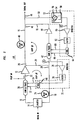
- FIG. 2 discloses feed-forward correction circuitry 10 and its use of information obtained from the pilot signal to reduce distortion produced by RF amplifier 12.
- An input signal for example including at least one carrier signal, is applied to a splitter 14.
- the splitter 14 replicates the input signal on a main signal path 16 and a feed forward path 18.
- the splitter 14 is part of a carrier cancellation loop referred to as loop # 1, which in addition to the splitter 14, comprises gain & phase circuit 20, coupler 22, the RF amplifier 12, delay circuit 24 and couplers 26 and 28.
- the signal on the main path 16 is applied to gain & phase circuit 20.
- the output of gain & phase circuit 20 and the pilot signal are applied to the coupler 22.
- the amplitude of the pilot signal is much less (e.g., 30 dB less) than the amplitude of the input signal so as not to interfere with the operation of the amplifier 12.
- the output of coupler 22 is applied to the amplifier 12 whose output comprises the amplified input signal, the amplified pilot signal and distortion signals produced by the amplifier 12.
- a portion of the output of the amplifier 12 is obtained from the coupler 26 and is combined at the coupler 28 via coupling path 30 with a delayed version of the input signal on the feed forward path 18 to isolate the pilot signal with distortion on the feed forward path 18.
- the input signal on the feed forward path 18 is sufficiently delayed by delay circuit 24 so that such signal experiences the same delay as the signal appearing at the coupler 28 via the path 30.
- the resulting error signal contains the distortion produced by the amplifier 12 along with any portion of the carrier signal remaining at the output of the coupler 28 and the pilot signal.
- the amount of carrier cancellation in the carrier cancellation loop depends on the proper gain and phase match between the two paths from the splitter 14 to the coupler 28.
- the gain & phase circuit 20 adjusts the phase and gain of the input signal according to control signals on control paths 32 and 34 such that the signal appearing at the coupler 28 via the path 30 is substantially the inverse (equal in amplitude but 180°out of phase) of the delayed input signal at the coupler 28.
- the gain and phase control signals appearing on the control paths 32 and 34 of the gain & phase circuit 20 are derived from the signal at the output of the coupler 28 in a well known manner using signal detection and control circuitry 35.
- the signal detection and control circuitry 35 detects an error signal for the carrier cancellation loop.
- the error signal represents the amplitude of the signal at point A, and the signal detection and control circuitry 35 attempts to reduce the amplitude of the error signal by providing gain and/or phase control signals.
- the signal detection and control circuitry 35 includes a detector 36, such as a log detector, which produces a signal representing the amplitude of the signal at point A.
- a filter 38 filters the output of the log detector to produce a DC-type amplitude signal representing the amplitude of the error signal.
- the amplitude signal is provided to a nulling circuit 40.
- the nulling circuit 40 provides the control signals on the control paths 32 and 34 to reduce the error signal, thereby reducing the carrier signal(s).
- the carrier signals combined at the coupler 28 substantially cancel each other leaving at the output of the coupler 28 the pilot signal with distortion produced by the amplifier 12.
- Loop # 1 is thus a carrier cancellation loop which serves to isolate on the feed forward path 18 the pilot signal with distortion produced by the amplifier 12.
- a distortion reduction loop or loop # 2 attempts to reduce the pilot signal on the main signal path 16, thereby reducing the distortion produced by the amplifier 12, using the error signal at the output of the coupler 28.
- the pilot signal with distortion on the feed forward path 18 is fed to a gain & phase circuit 42.
- the output of the gain and phase circuit 42 is fed to amplifier 44 whose output is applied to coupler 46.
- the coupler 46 combines the amplified pilot signal and distortion on the feed forward path 18 with the signals from the amplifier 12 on the main signal path 16 (carrier signal(s), pilot signal with distortion).
- a delay circuit 40 on the main signal path 16 delays the signals from the output of the amplifier 12 on the main signal path 16 to experience substantially the same delay as the corresponding signals from the output of the amplifier 12 which pass over the coupling path 30 through the coupler 28 to the coupler 46.
- a coupler 48 provides an error signal representative of the signal at the output of the coupler 46 onto a pilot detection path 50. Because the frequency, amplitude and other electrical characteristics of the pilot signal are known, pilot detection and control circuitry 52 can detect the amplitude of the remaining portion of the pilot signal from the error signal on the pilot detection path 50. The pilot detection and control circuitry 48 determines the amplitude of the pilot signal, and in response to the amplitude of the remaining pilot signal, the pilot detection and control circuitry 52 provides control signals to the phase and gain circuit 42.
- the pilot detection and control circuitry 48 will detect the pilot signal and use this information to generate control signals onto paths 66 and 68 to cause the gain & phase circuit 42 to modify the pilot signal on the feed forward path 18 such that the pilot signal on the main path 16 is substantially the inverse (equal in amplitude but 180° out of phase) of the pilot signal on the feed forward path 18 at the coupler 46.
- the corresponding pilot signals and distortion substantially cancel each other at the coupler 46 leaving the carrier signal(s) at the output of the system. Therefore, loop # 2 is a distortion reduction loop which attempts to cancel the pilot signal to cancel substantially the distortion produced by the amplifier 12.
- the pilot detection and control circuitry 52 includes pilot receive circuitry 54 which includes a mixer 56 to frequency convert the error signal on the pilot detection path 52 to lower frequencies and a filter 58 to facilitate detection of the pilot signal by a signal detector 60.
- the detector 60 such as a log detector, produces a signal representing the amplitude of the signal at point B.
- a filter 62 filters the output of the detector 60 to produce a DC-type amplitude signal representing the amplitude of the remaining pilot signal or error signal.
- the amplitude signal is provided to a nulling circuit 64. In response to the amplitude signal, the nulling circuit 64 provides control signals on the control paths 66 and 68 to the phase and gain circuit 42.
- the control signals are provided to reduce the amplitude signal, thereby reducing the remaining pilot signal.
- the amount of cancellation of the pilot signal indicates the amount of distortion cancellation.
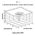
- the amount of signal cancellation depends on the proper gain and phase match between the combining signals.
- Signal reduction as a function of gain and phase mismatch is shown in FIG. 3 .
- the gain and phase characteristics of the amplifiers 12 and 44 as well as of the other devices vary over time. Such variations are typically due to the temperature, input power, device age and manufacturing variations.
- the signal detection and control circuitry 35 and the pilot detection and control circuitry 52 are designed to automatically control the gain and phase characteristics for the corresponding carrier cancellation and distortion reduction loops based on the amplitudes of the corresponding error signals.
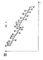
- the nulling circuits 40 and 64 attempt to reduce the error signal (indicating improved cancellation) by comparing every error signal sample with a previous error signal sample.
- the pilot detect and control circuitry 52 uses the pilot signal as a reference error signal.
- each nulling circuit makes two types of adjustments (gain and phase) based on the amplitude signal from one detector 36 or 60, and the nulling circuit 40 or 64 performs a series of n steps of phase adjustments (for example 12 steps) in sequence with n steps of gain adjustments. This alternating series of gain and phase adjustments is repeatedly performed to reduce the error signal toward null.
- the nulling circuit 40 or 64 determines how to adjust the phase or gain adjustment value (for example V.sub.out (n+ 1)) based on the results of the comparison between an error signal sample resulting from the last adjustment (for example error(n)) and the previous error signal sample (for example, error(n-1)).
- the phase or gain adjustment value for example V.sub.out (n+ 1)
- error(n) the last adjustment
- error(n-1) the previous error signal sample
- the nulling circuit makes a phase adjustment V.sub.phase (n+1) based on the previous error signal samples after steps 80k and 801 resulting from gain adjustments (for example, error.sub.gain (n)-error.sub.gain (n-1).
- gain adjustments for example, error.sub.gain (n)-error.sub.gain (n-1).
- the nulling circuit will make an incorrect phase adjustment based on the results of the last two gain adjustments, resulting in a jump 82 in the error signal.
- steps 84a-1 of phase adjustments bring the error signal back down, but the improper adjustment determination adversely effects the convergence rate.
- the nulling sensitivity and the location of the null varies as system parameters and transmit power varies.
- CDMA Code division multiple access
- TDMA Time division multiple access
- GSM Global System for Mobile Communications
- OFDM orthogonal frequency division multiplexing
- a linear amplifier should be able to react rapidly to transmit power changes and bursty traffic variations within the transient response specifications in the microsecond and millisecond ranges while providing adequate error cancellation.
- U.S. Patent No. 5,477,187 relates to a feed forward amplifier including a distortion extraction loop for extracting non-linear distortion components formed in a main amplifier and a distortion elimination loop for canceling out the distortion components by injecting the non-linear distortion components into an output signal of the main amplifier after modification.
- the feed forward amplifier controls the two loops independently for reducing the time needed for achieving control.
- the feed forward amplifier thereby facilitates a detection of failures, and the feed forward amplifier operates with reliability even under existence when a variation in the level incoming input signals exist.
- U.S. Patent No. 5,455,537 relates to a feed forward amplifier provided with an error sensing and correcting system which is particularly well suited for a minimizing distortions in an output of a feed forward amplifier introduced by a main amplifier of the feed forward amplifier.
- the feed forward amplifier also minimizes the pie requirements of an error amplifier of the feed forward amplifier.
- the present invention involves a gain and phase control system which performs a gain (or phase) adjustment based on the results of a previous gain (or phase) adjustment after an intervening phase (or gain) adjustment.
- a gain adjustment is based on the results of a previous gain adjustment rather than on the results of an intervening phase adjustment.
- a phase adjustment is based on the results of a previous phase adjustment rather than the results of an intervening gain adjustment.
- the gain and phase control system makes a gain (or phase) adjustment in parallel with detecting the results from a previous phase (or gain) adjustment, thereby taking advantage of the delay between adjustment and detection of the resulting error signal to improve the convergence rate.
- the gain and phase control system can perform single alternating gain and phase adjustments and make a gain (or phase) adjustment while detecting the error signal resulting from a preceding phase (or gain) adjustment.
- the gain and phase control system makes a phase (or gain) adjustment using the results detected from the preceding phase (or gain) adjustment.
- an illustrative embodiment of an alternating gain and phase control system is described with reference to a feed forward distortion reduction system.
- the next gain (or phase) adjustment is determined based on the results of the last gain (or phase) adjustment rather than on the result of the intervening phase (or gain) adjustment.
- the alternating gain and phase control system retains the results of the last gain adjustment, for example the magnitude of the resulting error signal, and determines the next gain adjustment based on the results of the last gain adjustment rather than the results of the preceding phase adjustment.
- the sign of the gain adjustment remains the same as the last gain adjustment. Otherwise, if the magnitude of the error signal resulting from the last gain adjustment increased compared to the previous error signal, the sign of the gain adjustment is changed.
- the gain and phase control system alternates between a gain adjustment and a phase adjustment by decoupling the performing of gain (or phase) adjustments and the detecting of the results of the preceding phase (or gain) adjustment.
- a gain (or phase) adjustment can be performed in parallel with the detection of the results of the preceding phase (or gain) adjustment. For example, while a gain adjustment (gain output of the null circuit) is being initiated, the error signal resulting from the preceding phase adjustment is being detected and processed. While the gain-adjusted signal experiences a propagation delay as it is amplified and combined and as the resulting error signal is detected and processed, a phase adjustment is initiated.
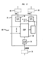
- FIG. 5 shows a general block diagram of an alternating gain and phase control circuitry 76 which receives an error signal representing the cancellation error for combining signals.
- the alternating gain and phase adjustment circuitry 76 reduces the error signal by providing the gain and phase adjustment control signals to make relative gain and phase adjustments between combining signals to improve the error cancellation of the combining signals.
- the alternating gain and phase adjustment system 76 can replace the nulling circuit 40 or 64 in the feed forward arrangement 10 ( FIG. 2 ).
- the alternating phase and gain adjustment circuitry 76 makes a previous gain (or phase) adjustment(s) followed by an intervening phase (or gain) adjustment(s), and the alternating gain and phase adjustment control 76 retains the results of the previous gain (or phase) adjustment, for example a magnitude for the resulting error signal, and determines the next gain (or phase) adjustment using the results of the previous gain (or phase) adjustment rather than the results of the intervening phase (or gain) adjustment.
- the sign of the gain (or phase) adjustment change ⁇ V(n+1) remains the same as the last gain (or phase) adjustment change ⁇ V(n). Otherwise, if the magnitude of the error signal error(n) resulting from the last gain (or phase) adjustment change ⁇ V(n) increased compared to the previous error signal error(n-1), the sign of the gain adjustment change ⁇ V(n+1) is changed.
- the alternating gain and phase control system 76 can make single alternating gain and phase adjustments, and a gain (or phase) adjustment can be performed in parallel with the detection of the results of the preceding phase (or gain) adjustment. Because the gain and phase adjustments have independent effects on the error signal, the alternating gain and phase control system 76 can take advantage of the propagation delay experienced by the gain- or phase-adjusted signal as the signal is amplified and combined and as the resulting error signal is detected, filtered and processed.
- a gain (or phase) adjustment can be performed in parallel with the detection of the results of the preceding phase (or gain) adjustment. Accordingly, in certain embodiments, the alternating gain and phase adjustment system makes a gain (or phase) adjustment while detecting the results of the preceding phase (or gain) adjustment. While the results from the gain (or phase) adjustment are being detected, a phase (or gain) adjustment is made based on the results of the previous phase (or gain) adjustment.
- alternating series of multiple gain and phase adjustments alternating single and/or multiple gain and phase adjustments and different or changing numbers of alternating gain and phase adjustment(s).
- the next gain (or phase) adjustment after an intervening series of phase (or gain) adjustments is based on the results of the last gain (or phase) adjustment before the series of phase (or gain) adjustments or before a single intervening gain (or phase) adjustment.
- embodiments can use previous system parameters, such as previous error signals or an error history for gain and/or phase adjustments, to make gain or phase adjustments.
- the error signal is analog-to-digitally converted by analog to digital (A/D) converter 78.
- A/D analog to digital
- an anti-aliasing filter 79 can be used to remove frequencies greater than 1/2 the A/D sampling frequency to improve detection of the signal representing the amplitude of the error signal.
- a DSP 80 receives the error signal and/or additional system information 82. In response to the error signal and/or other system information 82, the DSP 80 provides a gain or phase adjustment control signals attempting to reduce the error signal.
- the DSP 80 can use previous or cumulative information, such as error signal history, which can be stored in memory or storage 84 to determine a step size or adjustment factor as described in U.S. Patent No.
- the storage 84 can be integrated on the DSP 80 or electrically coupled thereto.
- the DSP 80 produces the gain and phase adjustment signals in digital form.
- a digital to analog (D/A) converter 86 converts the gain adjustment signals to analog form for a gain adjuster (not shown), and a digital to analog (D/A) converter 87 converts the phase adjustment signals to analog form for a phase adjuster (not shown).
- Reconstruction filters 88 and 89 can be used to respectively remove high frequency components from the output of the D/A's 86 and 87.
- the DSP 80 can also perform other control and calculations and provide additional gain and/or phase control signals (not shown) in response to a different error signal.
- the DSP 80 can be used to provide gain and/or phase control signals 32, 34, 66 and/or 68 ( FIG. 2 ) in response to the corresponding error signals at the input to the detection circuitry 35 and on the path 50.
- the alternating gain and phase adjustment control circuitry 76 can be implemented using discrete component(s), an integrated circuit(s) and/or software-driven processing circuitry.
- the negative sign in front of the equation flips the sign of the adjustment change ⁇ V gain (n+1) as compared to the sign of the previous gain adjustment change ⁇ V gain (n). If the sign of error gain (n)-error phase (n-1) is negative (meaning an improvement in the error signal from the last gain adjustment), the negative sign in front of the equation maintains the sign of the previous gain adjustment ⁇ V gain (n) which resulted in the improvement.
- K phase (n) is the same as K gain (n).
- the negative sign in front of the equation flips the sign of the adjustment change ⁇ V phase (n+1) as compared to the sign of the previous phase adjustment change ⁇ V phase (n). If the sign of error phase (n)-error gain (n-1) is negative (meaning an improvement in the error signal from the last phase adjustment), the negative sign in front of the equation maintains the sign of the previous phase adjustment ⁇ V phase (n) which resulted in the improvement.
- the gain (or phase) adjustment value V out (n+1) can be calculated by changing the previous gain (or phase) adjustment value V out (n) with a gain (or phase) adjustment change ⁇ V out (n+1).
- the gain adjustment value V gain (n+1) can be equal to V gain (n)+ ⁇ V gain (n+1), where V gain (n) is the previous gain adjustment value and ⁇ V gain (n+1) is the gain adjustment change.
- the previous adjustment value V gain (n) can be a fixed amount, an accumulation of adjustment changes or begins with a fixed amount which is changed by adjustment change(s).
- the adjustment value V out (n+1) can be calculated each time without using the magnitude of the previous adjustment value V out (n).
- the magnitude of the step-size or adjustment factor K(n+1) can be the magnitude of the adjustment change ⁇ V out (n+1) or the magnitude of the adjustment value V out (n+1).
- the adjustment value or change for phase and/or gain can be calculated using a fixed step size K(n+1) or an adaptive adjustment factor K(n+1).
- An adaptive step-size or adjustment factor is described in U.S. Patent No.
- embodiments of the alternating gain and phase control system improve the convergence rate by making a gain (or phase) adjustment using the results of the last gain (or phase) adjustment before an intervening phase (or gain) adjustment.
- the alternating gain and phase control system can perform single alternating gain and phase adjustments whereby a phase (or gain) adjustment is performed in parallel with the detection of the results of the previous gain (or phase) adjustment.
- the gain or phase adjustments can be determined differently for gain and phase adjustments.
- alternating gain and phase adjustment system according to the principles of the present invention are possible which omit and/or add components and/or use variations or portions of the described system.
- the embodiment of the alternating gain and phase control system has been described as being used with a particular feed-forward RF amplifier arrangement, but the alternating gain and phase control system can be used to improve the combining of signals in other amplifier or electrical circuit arrangements, and the combining signals could result in a constructive combination or resulting signal rather than a cancellation or error signal.
- particular embodiments are possible which determine an adjustment value, an adjustment change and/or an adjustment factor as described or in a different manner.
- an adjustment factor may be fixed which is used to determine an adjustment change which adjusts the previous adjustment value, adjusts relative to a fixed value without reference to the last or previous adjustment value(s) or is used as the adjustment value.
- the control system has been described as determining the adjustment value using the magnitude of the error signal or an error history, but depending on the application, the adjustment value can be determined based on other information, and the adjustment value can be changed in various ways.
- the gain and/or phase circuitry can be positioned in different locations and/or paths within the feed forward amplifier arrangement.
- the gain and phase adjustment circuit 20 could be located on the path 18 before the coupler 28; the gain and phase adjuster 42 could be located on the path 16 after the coupler 26; or gain and/or phase adjusters could be located on both paths.
- the control system has been described as using a software driven processing circuitry with analog and digital conversion, but other configurations can be implemented in application specific integrated circuits, software-driven processing circuitry, firmware or other arrangements of discrete components as would be understood by one of ordinary skill in the art with the benefit of this disclosure.
Landscapes
- Physics & Mathematics (AREA)
- Nonlinear Science (AREA)
- Engineering & Computer Science (AREA)
- Power Engineering (AREA)
- Amplifiers (AREA)
- Feedback Control In General (AREA)
Applications Claiming Priority (2)
| Application Number | Priority Date | Filing Date | Title |
|---|---|---|---|
| US378009 | 1982-05-13 | ||
| US09/378,009 US6392480B1 (en) | 1999-08-19 | 1999-08-19 | Alternating gain and phase control system and method |
Publications (3)
| Publication Number | Publication Date |
|---|---|
| EP1079516A2 EP1079516A2 (en) | 2001-02-28 |
| EP1079516A3 EP1079516A3 (en) | 2001-10-31 |
| EP1079516B1 true EP1079516B1 (en) | 2010-01-13 |
Family
ID=23491363
Family Applications (1)
| Application Number | Title | Priority Date | Filing Date |
|---|---|---|---|
| EP00306694A Expired - Lifetime EP1079516B1 (en) | 1999-08-19 | 2000-08-07 | Alternating gain and phase control system and method |
Country Status (9)
| Country | Link |
|---|---|
| US (1) | US6392480B1 (enExample) |
| EP (1) | EP1079516B1 (enExample) |
| JP (1) | JP2001119249A (enExample) |
| KR (1) | KR20010021355A (enExample) |
| CN (1) | CN100452643C (enExample) |
| AU (1) | AU765299B2 (enExample) |
| BR (1) | BR0003387B1 (enExample) |
| CA (1) | CA2315583C (enExample) |
| DE (1) | DE60043683D1 (enExample) |
Families Citing this family (6)
| Publication number | Priority date | Publication date | Assignee | Title |
|---|---|---|---|---|
| US6411644B1 (en) * | 1998-09-29 | 2002-06-25 | Lucent Technologies Inc. | Frequency hop pilot technique for a control system that reduces distortion produced by electrical circuits |
| JP2003110369A (ja) * | 2001-09-27 | 2003-04-11 | Hitachi Kokusai Electric Inc | 歪み補償増幅装置 |
| EP1552605A4 (en) * | 2002-06-25 | 2007-05-30 | Soma Networks Inc | AMPLIFIERS WITH DOWNSTREAM CORRECTION |
| US6882217B1 (en) | 2002-09-27 | 2005-04-19 | 3Com Corporation | Cubic spline predistortion, algorithm and training, for a wireless LAN system |
| US7274750B1 (en) | 2002-09-27 | 2007-09-25 | 3Com Corporation | Gain and phase imbalance compensation for OFDM systems |
| US9473275B2 (en) | 2013-11-13 | 2016-10-18 | Mediatek Singapore Pte. Ltd. | Gain asymmetry characterizing circuit and method for determining characteristics of gain asymmetry possessed by transmitter |
Family Cites Families (15)
| Publication number | Priority date | Publication date | Assignee | Title |
|---|---|---|---|---|
| JPH04275708A (ja) * | 1991-03-01 | 1992-10-01 | Nippon Telegr & Teleph Corp <Ntt> | 非線形歪補償回路 |
| US5477187A (en) | 1992-03-19 | 1995-12-19 | Fujitsu Limited | Feed forward amplifier |
| US5365190A (en) * | 1993-05-03 | 1994-11-15 | Duly Research, Inc. | Feed-forward digital phase and amplitude correction system |
| US5485120A (en) * | 1994-07-28 | 1996-01-16 | Aval Communications Inc. | Feed-forward power amplifier system with adaptive control and control method |
| US5610554A (en) * | 1994-07-28 | 1997-03-11 | Aval Communications Inc. | Cancellation loop, for a feed-forward amplifier, employing an adaptive controller |
| US5455537A (en) * | 1994-08-19 | 1995-10-03 | Radio Frequency Systems, Inc. | Feed forward amplifier |
| JP3361657B2 (ja) * | 1995-07-20 | 2003-01-07 | 松下電器産業株式会社 | フィードフォワード増幅器の制御装置および制御方法 |
| KR100217416B1 (ko) | 1995-11-16 | 1999-09-01 | 윤종용 | 선형 증폭 장치 및 방법 |
| US5789976A (en) * | 1996-06-17 | 1998-08-04 | Corporation De L'ecole Polytechnique | Digital adaptive control of feedforward amplifier using frequency domain cancellation |
| US5847603A (en) * | 1997-07-31 | 1998-12-08 | Lucent Technologies Inc. | Automatic control system for reducing distortion produced by electrical circuits |
| US5999048A (en) * | 1998-01-13 | 1999-12-07 | Lucent Technologies Inc. | Method and apparatus for spread spectrum pilot extraction for RF amplifiers |
| US5929704A (en) * | 1998-02-20 | 1999-07-27 | Spectrian | Control of RF error extraction using auto-calibrating RF correlator |
| US5963091A (en) * | 1998-04-01 | 1999-10-05 | Chen; Jiunn-Tsair | Article comprising a power amplifier with feed forward linearizer using a RLS parameter tracking algorithm |
| JP2000004124A (ja) * | 1998-06-17 | 2000-01-07 | Nec Corp | フィードフォワード増幅器 |
| US6211733B1 (en) * | 1999-10-22 | 2001-04-03 | Powerwave Technologies, Inc. | Predistortion compensation for a power amplifier |
-
1999
- 1999-08-19 US US09/378,009 patent/US6392480B1/en not_active Expired - Lifetime
-
2000
- 2000-08-07 DE DE60043683T patent/DE60043683D1/de not_active Expired - Lifetime
- 2000-08-07 EP EP00306694A patent/EP1079516B1/en not_active Expired - Lifetime
- 2000-08-08 BR BRPI0003387-1B1A patent/BR0003387B1/pt not_active IP Right Cessation
- 2000-08-08 CA CA002315583A patent/CA2315583C/en not_active Expired - Fee Related
- 2000-08-09 JP JP2000240717A patent/JP2001119249A/ja not_active Abandoned
- 2000-08-11 AU AU51968/00A patent/AU765299B2/en not_active Ceased
- 2000-08-18 KR KR1020000047856A patent/KR20010021355A/ko not_active Ceased
- 2000-08-18 CN CNB001241664A patent/CN100452643C/zh not_active Expired - Fee Related
Also Published As
| Publication number | Publication date |
|---|---|
| JP2001119249A (ja) | 2001-04-27 |
| CA2315583A1 (en) | 2001-02-19 |
| CN1289177A (zh) | 2001-03-28 |
| DE60043683D1 (de) | 2010-03-04 |
| EP1079516A2 (en) | 2001-02-28 |
| CN100452643C (zh) | 2009-01-14 |
| US6392480B1 (en) | 2002-05-21 |
| EP1079516A3 (en) | 2001-10-31 |
| CA2315583C (en) | 2005-02-08 |
| BR0003387A (pt) | 2001-04-03 |
| AU765299B2 (en) | 2003-09-11 |
| AU5196800A (en) | 2001-02-22 |
| KR20010021355A (ko) | 2001-03-15 |
| BR0003387B1 (pt) | 2013-06-25 |
Similar Documents
| Publication | Publication Date | Title |
|---|---|---|
| EP1262017B1 (en) | Spectral distortion monitor for controlling pre-distortion and feed-forward linearization of rf power amplifier | |
| EP0541789B1 (en) | Feed forward amplifier network with frequency swept pilot tone | |
| EP1777813B1 (en) | Adaptive gain and/or phase adjustment control method | |
| US7791413B2 (en) | Linearizing technique for power amplifiers | |
| US5986499A (en) | Pilot signal detection system using band reject filter | |
| JPH0878965A (ja) | フィードフォワード増幅器 | |
| WO1992012571A1 (en) | A method and apparatus for optimizing the performance of a power amplifier circuit | |
| KR100390073B1 (ko) | 초선형 피드포워드 rf 전력 증폭기 | |
| EP0797868A1 (en) | Amplifier circuit for rf system | |
| EP1079516B1 (en) | Alternating gain and phase control system and method | |
| JP4896424B2 (ja) | 歪補償増幅器 | |
| US6236286B1 (en) | Integrated on-board automated alignment for a low distortion amplifier | |
| US6166600A (en) | Automatic gain and phase controlled feedforward amplifier without pilot signal | |
| US6545487B1 (en) | System and method for producing an amplified signal with reduced distortion | |
| JP2007013230A (ja) | 歪補償増幅回路 |
Legal Events
| Date | Code | Title | Description |
|---|---|---|---|
| PUAI | Public reference made under article 153(3) epc to a published international application that has entered the european phase |
Free format text: ORIGINAL CODE: 0009012 |
|
| AK | Designated contracting states |
Kind code of ref document: A2 Designated state(s): AT BE CH CY DE DK ES FI FR GB GR IE IT LI LU MC NL PT SE |
|
| AX | Request for extension of the european patent |
Free format text: AL;LT;LV;MK;RO;SI |
|
| PUAL | Search report despatched |
Free format text: ORIGINAL CODE: 0009013 |
|
| AK | Designated contracting states |
Kind code of ref document: A3 Designated state(s): AT BE CH CY DE DK ES FI FR GB GR IE IT LI LU MC NL PT SE |
|
| AX | Request for extension of the european patent |
Free format text: AL;LT;LV;MK;RO;SI |
|
| 17P | Request for examination filed |
Effective date: 20020420 |
|
| AKX | Designation fees paid |
Free format text: DE FI FR GB SE |
|
| 17Q | First examination report despatched |
Effective date: 20051227 |
|
| APBK | Appeal reference recorded |
Free format text: ORIGINAL CODE: EPIDOSNREFNE |
|
| APBN | Date of receipt of notice of appeal recorded |
Free format text: ORIGINAL CODE: EPIDOSNNOA2E |
|
| APBR | Date of receipt of statement of grounds of appeal recorded |
Free format text: ORIGINAL CODE: EPIDOSNNOA3E |
|
| APBV | Interlocutory revision of appeal recorded |
Free format text: ORIGINAL CODE: EPIDOSNIRAPE |
|
| GRAP | Despatch of communication of intention to grant a patent |
Free format text: ORIGINAL CODE: EPIDOSNIGR1 |
|
| RAP3 | Party data changed (applicant data changed or rights of an application transferred) |
Owner name: LUCENT TECHNOLOGIES INC. |
|
| GRAS | Grant fee paid |
Free format text: ORIGINAL CODE: EPIDOSNIGR3 |
|
| GRAA | (expected) grant |
Free format text: ORIGINAL CODE: 0009210 |
|
| AK | Designated contracting states |
Kind code of ref document: B1 Designated state(s): DE FI FR GB SE |
|
| REG | Reference to a national code |
Ref country code: GB Ref legal event code: FG4D |
|
| REF | Corresponds to: |
Ref document number: 60043683 Country of ref document: DE Date of ref document: 20100304 Kind code of ref document: P |
|
| PG25 | Lapsed in a contracting state [announced via postgrant information from national office to epo] |
Ref country code: FI Free format text: LAPSE BECAUSE OF FAILURE TO SUBMIT A TRANSLATION OF THE DESCRIPTION OR TO PAY THE FEE WITHIN THE PRESCRIBED TIME-LIMIT Effective date: 20100113 |
|
| PG25 | Lapsed in a contracting state [announced via postgrant information from national office to epo] |
Ref country code: SE Free format text: LAPSE BECAUSE OF FAILURE TO SUBMIT A TRANSLATION OF THE DESCRIPTION OR TO PAY THE FEE WITHIN THE PRESCRIBED TIME-LIMIT Effective date: 20100113 |
|
| PLBE | No opposition filed within time limit |
Free format text: ORIGINAL CODE: 0009261 |
|
| STAA | Information on the status of an ep patent application or granted ep patent |
Free format text: STATUS: NO OPPOSITION FILED WITHIN TIME LIMIT |
|
| 26N | No opposition filed |
Effective date: 20101014 |
|
| REG | Reference to a national code |
Ref country code: GB Ref legal event code: 732E Free format text: REGISTERED BETWEEN 20131128 AND 20131204 |
|
| REG | Reference to a national code |
Ref country code: FR Ref legal event code: CD Owner name: ALCATEL-LUCENT USA INC. Effective date: 20131122 |
|
| REG | Reference to a national code |
Ref country code: FR Ref legal event code: GC Effective date: 20140410 |
|
| REG | Reference to a national code |
Ref country code: FR Ref legal event code: RG Effective date: 20141015 |
|
| REG | Reference to a national code |
Ref country code: FR Ref legal event code: PLFP Year of fee payment: 16 |
|
| PGFP | Annual fee paid to national office [announced via postgrant information from national office to epo] |
Ref country code: DE Payment date: 20150821 Year of fee payment: 16 Ref country code: GB Payment date: 20150819 Year of fee payment: 16 |
|
| PGFP | Annual fee paid to national office [announced via postgrant information from national office to epo] |
Ref country code: FR Payment date: 20150820 Year of fee payment: 16 |
|
| REG | Reference to a national code |
Ref country code: DE Ref legal event code: R119 Ref document number: 60043683 Country of ref document: DE |
|
| GBPC | Gb: european patent ceased through non-payment of renewal fee |
Effective date: 20160807 |
|
| REG | Reference to a national code |
Ref country code: FR Ref legal event code: ST Effective date: 20170428 |
|
| PG25 | Lapsed in a contracting state [announced via postgrant information from national office to epo] |
Ref country code: GB Free format text: LAPSE BECAUSE OF NON-PAYMENT OF DUE FEES Effective date: 20160807 Ref country code: DE Free format text: LAPSE BECAUSE OF NON-PAYMENT OF DUE FEES Effective date: 20170301 Ref country code: FR Free format text: LAPSE BECAUSE OF NON-PAYMENT OF DUE FEES Effective date: 20160831 |