EP1079467A1 - Component for mounting on a circuit board - Google Patents
Component for mounting on a circuit board Download PDFInfo
- Publication number
- EP1079467A1 EP1079467A1 EP00117742A EP00117742A EP1079467A1 EP 1079467 A1 EP1079467 A1 EP 1079467A1 EP 00117742 A EP00117742 A EP 00117742A EP 00117742 A EP00117742 A EP 00117742A EP 1079467 A1 EP1079467 A1 EP 1079467A1
- Authority
- EP
- European Patent Office
- Prior art keywords
- component
- circuit board
- anchoring device
- electrical connector
- printed circuit
- Prior art date
- Legal status (The legal status is an assumption and is not a legal conclusion. Google has not performed a legal analysis and makes no representation as to the accuracy of the status listed.)
- Ceased
Links
Images

Classifications
-
- H—ELECTRICITY
- H01—ELECTRIC ELEMENTS
- H01R—ELECTRICALLY-CONDUCTIVE CONNECTIONS; STRUCTURAL ASSOCIATIONS OF A PLURALITY OF MUTUALLY-INSULATED ELECTRICAL CONNECTING ELEMENTS; COUPLING DEVICES; CURRENT COLLECTORS
- H01R12/00—Structural associations of a plurality of mutually-insulated electrical connecting elements, specially adapted for printed circuits, e.g. printed circuit boards [PCB], flat or ribbon cables, or like generally planar structures, e.g. terminal strips, terminal blocks; Coupling devices specially adapted for printed circuits, flat or ribbon cables, or like generally planar structures; Terminals specially adapted for contact with, or insertion into, printed circuits, flat or ribbon cables, or like generally planar structures
- H01R12/70—Coupling devices
- H01R12/7005—Guiding, mounting, polarizing or locking means; Extractors
- H01R12/7011—Locking or fixing a connector to a PCB
- H01R12/707—Soldering or welding
-
- H—ELECTRICITY
- H01—ELECTRIC ELEMENTS
- H01R—ELECTRICALLY-CONDUCTIVE CONNECTIONS; STRUCTURAL ASSOCIATIONS OF A PLURALITY OF MUTUALLY-INSULATED ELECTRICAL CONNECTING ELEMENTS; COUPLING DEVICES; CURRENT COLLECTORS
- H01R12/00—Structural associations of a plurality of mutually-insulated electrical connecting elements, specially adapted for printed circuits, e.g. printed circuit boards [PCB], flat or ribbon cables, or like generally planar structures, e.g. terminal strips, terminal blocks; Coupling devices specially adapted for printed circuits, flat or ribbon cables, or like generally planar structures; Terminals specially adapted for contact with, or insertion into, printed circuits, flat or ribbon cables, or like generally planar structures
- H01R12/70—Coupling devices
- H01R12/71—Coupling devices for rigid printing circuits or like structures
- H01R12/72—Coupling devices for rigid printing circuits or like structures coupling with the edge of the rigid printed circuits or like structures
- H01R12/721—Coupling devices for rigid printing circuits or like structures coupling with the edge of the rigid printed circuits or like structures cooperating directly with the edge of the rigid printed circuits
-
- H—ELECTRICITY
- H05—ELECTRIC TECHNIQUES NOT OTHERWISE PROVIDED FOR
- H05K—PRINTED CIRCUITS; CASINGS OR CONSTRUCTIONAL DETAILS OF ELECTRIC APPARATUS; MANUFACTURE OF ASSEMBLAGES OF ELECTRICAL COMPONENTS
- H05K3/00—Apparatus or processes for manufacturing printed circuits
- H05K3/30—Assembling printed circuits with electric components, e.g. with resistor
- H05K3/303—Surface mounted components, e.g. affixing before soldering, aligning means, spacing means
-
- H—ELECTRICITY
- H05—ELECTRIC TECHNIQUES NOT OTHERWISE PROVIDED FOR
- H05K—PRINTED CIRCUITS; CASINGS OR CONSTRUCTIONAL DETAILS OF ELECTRIC APPARATUS; MANUFACTURE OF ASSEMBLAGES OF ELECTRICAL COMPONENTS
- H05K3/00—Apparatus or processes for manufacturing printed circuits
- H05K3/30—Assembling printed circuits with electric components, e.g. with resistor
- H05K3/32—Assembling printed circuits with electric components, e.g. with resistor electrically connecting electric components or wires to printed circuits
- H05K3/34—Assembling printed circuits with electric components, e.g. with resistor electrically connecting electric components or wires to printed circuits by soldering
- H05K3/341—Surface mounted components
- H05K3/3421—Leaded components
Definitions
- the present invention relates to a device according to the Preamble of claim 1, i.e. one for mounting on a printed circuit board component, with connection elements, through which the component at least electrically with the circuit board is connectable, and with an anchoring device, through which the component can be mechanically connected to the circuit board is.
- Components of this type are in a variety of forms known. This is particularly mechanical stressed components such as electrical Interconnects.
- the connecting elements through which the relevant components are at least electrically connected to the circuit board are often connection elements that are designed to soldered to the circuit board after an SMT soldering process become.
- anchoring device are provided on the relevant component locking hook, which at Assembly of the component on the printed circuit board with assigned Locking elements of the circuit board (for example, in the The recesses provided).
- Such and similar anchoring devices connect the component and the circuit board, however, is not completely tight with each other. There is always a certain game, which causes movement of the component relative to the circuit board is not entirely excluded are. Even very little freedom of movement can over time lead to a detachment of the connection elements of the component from the circuit board.
- Anchoring devices already exist that have this disadvantage do not have. Such anchoring devices are for example brackets or the like holding mechanisms that screwed or soldered to the circuit board. Anchoring devices of this type are, for example, from the GB 2 300 313 A, US 5 541 384 and DE 197 43 251 C1. As can be seen from the publications mentioned, enlarge such anchoring devices that contain them Components and / or limit the freedom of design in component and / or circuit design (for example such components can not be arranged directly next to each other become).
- From EP 0 532 974 is one on a printed circuit board fixed component known in the form of a connector, in the extension of side walls of the cuboid Component feet are formed, which in the holes Protrude PCB. The bottom ends of the feet are separated, a part is to form one under the Printed circuit board snapping snap-in hook, another Part runs smoothly through the hole in the PCB and will go away from the layout of the component Conductor tracks over melted solder paste electrically and mechanically connected. This component also prohibits one compact arrangement of several components on the PCB because of the mechanical / electrical connection considerable part over the outline of the component to the outside leads away.
- From DE 197 43 251 C1 is for mounting on a Printed circuit board designed component known in the below Anchoring elements of the component are provided, of which projections outward beyond the outline of the component stick out over solder paste with the top of one PCB are connected.
- the present invention is therefore based on the object the component according to the preamble of claim 1 such to further develop that the component is not or in any case not significantly increasing and the freedom of design component and / or circuit design anchoring device which does not restrict or at least does not significantly restrict it so connectable to the circuit board is that the electrical connection between the component and movements of the component impairing the printed circuit board Reliably and permanently excluded relative to the circuit board are.
- the anchoring device so is trained and arranged so that it is at one under the Component lying point can be soldered to the circuit board.
- An anchoring device designed and arranged in this way does not make the component larger, nor does it impair it the freedom of design in component and / or circuit design.
- this type can be reliably ensured that the electrical Connection between the component and the circuit board impairing Movements of the component relative to the circuit board are reliably and permanently excluded.
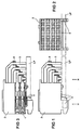
- the electrical connector under consideration consists of a front one Section V and a rear section H and is for this designed, only with the rear section H on a circuit board LP to be put on; the front section V stands in the state of the electrical placed on the circuit board Connector laterally over the PCB LP. Indeed there is no restriction.
- the following closer Peculiarities of the electrical connector described can also be provided for components that do not have the Protect the circuit board.
- the electrical connector under consideration essentially exists from contact elements 1, a housing 2 accommodating them, electrical connection elements led out of the housing 2 3, one of the connection elements 3 in a predetermined Relativiage fixing alignment plate 4, and an anchoring device 5.
- the contact elements 1 serve to connect the electrical Connector with another electrical connector. Such Contact elements are known and do not require any further explanation.
- connection elements 3 serve for the electrical connection of the electrical connector to the PCB LP.
- connection elements 3 serve for the electrical connection of the electrical connector to the PCB LP.
- Example is for surface mounting of the electrical connector on the printed circuit board SMT contacts.
- the alignment plate 4 serves, as already mentioned above was used to fix the connection elements 3 in a predetermined Relative position.
- Alignment plate 4 is referred to DE 197 54 877 A1.
- the anchoring device 5 serves the electrical Connect the connector mechanically to the circuit board. It ensures that the electrical connection between the electrical connector and the circuit board (the Connections between the connection elements 3 and the circuit board LP) impairing movements of the electrical connector Relative and permanent relative to the circuit board excluded are.
- the anchoring device 5 is in the example considered through a material consisting of metal or metal, plate-like body with a widened Place formed downward curved edge sections. She is on the housing 2 or another component of the electrical Fastened connector and has one for soldering to the Printed circuit board LP designed part.
- the anchoring device is attached 5 on the housing 2 by partial pouring the anchoring device 5 in the housing 2.
- the not cast part of the anchoring device runs in the considered Example along the bottom of the case base and at least partially forms the one to be soldered to the PCB designed part of the anchoring device.
- the part of the PCB designed for soldering Anchoring device 5 is one at the bottom of the floor the housing 2 along, essentially extending over the entire width of the electrical connector Stripes.
- the anchoring device 5 is preferred also designed to use an SMT process to be connected to the circuit board surface. This is also the case in the example considered. However, there is no limitation to this.
- the anchoring device can in principle also after any other Procedure to be soldered to the circuit board.
- anchoring device 5 as in the example considered soldered to the circuit board using an SMT process is, for example, using the so-called BGA (Ball Grid Array) technology or the so-called PSGA (Plastic Stud Grid Array) technology.
- the anchoring device 5 can by a corresponding Training the same can be assigned a double function: with appropriate training, it can also be used as an or several shielding contact elements act with associated Contact elements one with your electrical connector in contact other electrical connector to be brought into contact can be brought.
- An electrical connector with a such anchoring device is shown in FIGS. 4 to 6 shown.
- the electrical connector shown in Figures 4 to 6 corresponds to the in the anchoring device 5 in the Figures 1 to 3 electrical connector shown; with the Elements designated by the same reference numerals are corresponding to one another Elements.
- the statements made above for the anchoring device 5 have also according to the electrical connector 4 to 6 provided anchoring device Validity.
- the electrical connector anchoring device according to Figures 4 to 6 differs from that Anchoring device of the electrical connector according to the Figures 1 to 3 "only" in that the anchoring device of the electrical connector according to FIGS. 4 to 6 have outlets designated by the reference number 6, which itself - through the connector housing and / or inside or running along the outside of the connector housing - as in the Figures 4 to 6 shown or similar in the front section V of the electrical connector.
- the end sections 61 of the foothills 6 are freely accessible sections the foothills and are designed as contact elements that with assigned contact elements one with the one under consideration electrical connectors to be brought into contact Connector can be brought into contact.
- the formed by the anchoring device or by these outgoing contact elements are preferably shielded contacts used by which one at the electrical Shielding device provided for connectors or connecting lines for shielding electromagnetic radiation to a certain potential (preferably ground potential) can be brought.
- the application of the concerned Contact elements with the predetermined potential can over the PCB carrying the electrical connector, more specifically done through the solder joint through which the electrical Printed circuit board and the anchoring device connected to each other are.
- anchorage device formed or outgoing contact elements also for the transfer of potentials required for other purposes, Signals and / or data are used.
- Anchoring device especially its size, its shape etc.
- connection of the anchoring device with the housing or other component parts varied is modifiable.
- Components designed as described can be independent of the details of the practical implementation without or at any rate without significant enlargement of the component and without or in any case without any significant restriction on the freedom of design in component and / or circuit design in this way be connected to the circuit board that the electrical Connection between the component and the circuit board impairing Movements of the component relative to the circuit board are reliably and permanently excluded.
Landscapes
- Coupling Device And Connection With Printed Circuit (AREA)
Abstract
Description
Die vorliegende Erfindung betrifft eine Vorrichtung gemäß dem Oberbegriff des Patentanspruchs 1, d.h. ein zur Montage auf eine Leiterplatte ausgelegtes Bauteil, mit Anschlußelementen, durch welche das Bauteil zumindest elektrisch mit der Leiterplatte verbindbar ist, und mit einer Verankerungsvorrichtung, durch welche das Bauteil mechanisch mit der Leiterplatte verbindbar ist.The present invention relates to a device according to the Preamble of claim 1, i.e. one for mounting on a printed circuit board component, with connection elements, through which the component at least electrically with the circuit board is connectable, and with an anchoring device, through which the component can be mechanically connected to the circuit board is.
Bauteile dieser Art sind in einer Vielzahl von Ausführungsformen bekannt. Dabei handelt es sich insbesondere um mechanisch beanspruchte Bauteile wie beispielsweise elektrische Verbinder.Components of this type are in a variety of forms known. This is particularly mechanical stressed components such as electrical Interconnects.
Die Anschlußelemente, durch welche die betreffenden Bauteile zumindest elektrisch mit der Leiterplatte verbunden werden, sind dabei häufig Anschlußelemente, die dazu ausgelegt sind, nach einem SMT-Lötverfahren mit der Leiterplatte verlötet zu werden.The connecting elements through which the relevant components are at least electrically connected to the circuit board, are often connection elements that are designed to soldered to the circuit board after an SMT soldering process become.
Insbesondere bei derart ausgebildeten, aber auch bei andersartigen Anschlußelementen besteht die Gefahr, daß diese sich bei einer starken mechanischen Beanspruchung des Bauteils (bei einer Bewegung des Bauteils relativ zur Leiterplatte, beispielsweise beim Einstecken eines elektrischen Verbinders in einen auf der Leiterplatte montierten elektrischen Verbinder) von der Leiterplatte ablösen, wodurch der elektrische Kontakt zu dieser zeitweise oder dauerhaft unterbrochen oder zumindest verschlechtert wird.Especially with such trained, but also with other types There is a risk of connecting elements that these when the component is subjected to high mechanical stress (when the component moves relative to the circuit board, for example when an electrical connector is inserted into an electrical connector mounted on the circuit board) detach from the circuit board, causing the electrical Contact with this temporarily or permanently interrupted or is at least worsening.
Zur Vermeidung dessen sind solche Bauteile zum Teil mit Verankerungsvorrichtungen ausgestattet, durch welche sie mechanisch so fest mit der Leiterplatte verbunden werden sollen, daß eine Bewegung relativ zur Leiterplatte ausgeschlossen oder zumindest erheblich eingeschränkt ist.To avoid this, such components are partly with anchoring devices equipped by which they are mechanically should be so firmly connected to the circuit board that movement relative to the circuit board is excluded or is at least significantly restricted.
Ein Beispiel für eine derartige Verankerungsvorrichtung sind am betreffenden Bauteil vorgesehene Rasthaken, welche bei der Montage des Bauteils auf die Leiterplatte mit zugeordneten Rastelementen der Leiterplatte (beispielsweise mit in der Leiterplatte vorgesehenen Ausnehmungen) verrasten. Derartige und ähnliche Verankerungsvorrichtungen verbinden das Bauteil und die Leiterplatte jedoch nicht vollkommen fest miteinander. Es ist immer ein gewisses Spiel vorhanden, wodurch Bewegungen des Bauteils relativ zur Leiterplatte nicht gänzlich ausgeschlossen sind. Selbst sehr kleine Bewegungsfreiheiten können mit der Zeit zu einer Ablösung der Anschlußelemente des Bauteils von der Leiterplatte führen.An example of such anchoring device are provided on the relevant component locking hook, which at Assembly of the component on the printed circuit board with assigned Locking elements of the circuit board (for example, in the The recesses provided). Such and similar anchoring devices connect the component and the circuit board, however, is not completely tight with each other. There is always a certain game, which causes movement of the component relative to the circuit board is not entirely excluded are. Even very little freedom of movement can over time lead to a detachment of the connection elements of the component from the circuit board.
Es gibt bereits Verankerungsvorrichtungen, die diesen Nachteil
nicht aufweisen. Solche Verankerungsvorrichtungen sind
beispielsweise Bügel oder dergleichen Haltemechanismen, die
mit der Leiterplatte verschraubt oder verlötet werden. Verankerungsvorrichtungen
dieser Art sind beispielsweise aus der
GB 2 300 313 A, der US 5 541 384 und der DE 197 43 251 C1 bekannt.
Wie aus den genannten Druckschriften ersichtlich ist,
vergrößern solche Verankerungsvorrichtungen die diese enthaltenden
Bauteile und/oder schränken die Gestaltungsfreiheit
beim Bauteil- und/oder Schaltungsentwurf ein (beispielsweise
können solche Bauteile nicht unmittelbar nebeneinander angeordnet
werden).Anchoring devices already exist that have this disadvantage
do not have. Such anchoring devices are
for example brackets or the like holding mechanisms that
screwed or soldered to the circuit board. Anchoring devices
of this type are, for example, from the
Aus der EP 0 532 974 ist ein auf einer Leiterplatte befestigtes Bauteil in Form eines Steckverbinders bekannt, bei dem in Verlängerung von Seitenwänden des quaderförmigen Bauteils Füße ausgebildet sind, welche in Bohrungen der Leiterplatte hineinragen. Die unteren Enden der Füße sind aufgetrennt, ein Teil ist zur Ausbildung eines unter die Leiterplatte schnappenden Rasthakens abgeknickt, ein anderer Teil verläuft glatt durch die Bohrung der Leiterplatte und wird mit von dem Grundriß des Bauteils nach außen weggehenden Leiterbahnen über angeschmolzene Lötpaste elektrisch und mechanisch verbunden. Auch dieses Bauteil verbietet eine kompakte Aneinanderreihung mehrerer Bauteile auf der Leiterplatte, da die mechanische/elektrische Verbindung ein beträchtliches Stück über den Umriß des Bauteils nach außen wegführt.From EP 0 532 974 is one on a printed circuit board fixed component known in the form of a connector, in the extension of side walls of the cuboid Component feet are formed, which in the holes Protrude PCB. The bottom ends of the feet are separated, a part is to form one under the Printed circuit board snapping snap-in hook, another Part runs smoothly through the hole in the PCB and will go away from the layout of the component Conductor tracks over melted solder paste electrically and mechanically connected. This component also prohibits one compact arrangement of several components on the PCB because of the mechanical / electrical connection considerable part over the outline of the component to the outside leads away.
Aus der DE 36 37 190 A1 ist ein auf einer Leiterplatte durch Rastfüße verankertes Bauteil bekannt. Die Rastfüße können außerhalb des eigentlichen Bauteils, jedoch auch in dem Umriß des Bauteils integriert sein (Spalte 4, Zeilen 31-37) . Die Besonderheit dieses bekannten Bauteils besteht in der teilhülsenförmigen Ausbildung der auf der Unterseite der Leiterplatte abstehenden Rastfüße. Durch Einfädeln eines Werkzeugs an der Oberseite (an dem Bauteil vorbei) wird das hülsenförmige Ende des in die Leiterplatte eingesteckten Fußes aufgeweitet und hat damit eine größere Abmessung als der Durchmesser des in der Leiterplatte befindlichen Aufnahmelochs.From DE 36 37 190 A1 one is on a circuit board Locking feet anchored component known. The locking feet can outside the actual component, but also in the outline of the component must be integrated (column 4, lines 31-37). The A special feature of this known component is the partial sleeve Training on the bottom of the PCB protruding locking feet. By threading one Tool on the top (past the component) that will sleeve-shaped end of the inserted in the circuit board Expanded foot and thus has a larger dimension than the diameter of the one in the circuit board Receiving hole.
Aus der DE 197 43 251 C1 ist ein zur Montage auf einer Leiterplatte ausgelegtes Bauteil bekannt, bei dem unterhalb des Bauteils Verankerungselemente vorgesehen sind, von denen nach außen über den Umriß des Bauteils hinaus Fortsätze abstehen, die über Lötpaste mit der Oberseite einer Leiterplatte verbunden werden.From DE 197 43 251 C1 is for mounting on a Printed circuit board designed component known in the below Anchoring elements of the component are provided, of which projections outward beyond the outline of the component stick out over solder paste with the top of one PCB are connected.
Der vorliegenden Erfindung liegt daher die Aufgabe zugrunde, das Bauteil gemäß dem Oberbegriff des Patentanspruchs 1 derart weiterzubilden, daß dieses durch eine das Bauteil nicht oder jedenfalls nicht nennenswert vergrößernde und die Gestaltungsfreiheit beim Bauteil- und/oder Schaltungsentwurf nicht oder jedenfalls nicht nennenswert einschränkende Verankerungsvorrichtung derart mit der Leiterplatte verbindbar ist, daß die elektrische Verbindung zwischen dem Bauteil und der Leiterplatte beeinträchtigende Bewegungen des Bauteils relativ zur Leiterplatte zuverlässig und dauerhaft ausgeschlossen sind.The present invention is therefore based on the object the component according to the preamble of claim 1 such to further develop that the component is not or in any case not significantly increasing and the freedom of design component and / or circuit design anchoring device which does not restrict or at least does not significantly restrict it so connectable to the circuit board is that the electrical connection between the component and movements of the component impairing the printed circuit board Reliably and permanently excluded relative to the circuit board are.
Diese Aufgabe wird erfindungsgemäß durch die im kennzeichnenden Teil des Patentanspruchs 1 beanspruchten Merkmale gelöst.This object is achieved by the characterizing Part of claim 1 claimed features solved.
Demnach ist vorgesehen, daß die Verankerungsvorrichtung so ausgebildet und angeordnet ist, daß sie an einer unter dem Bauteil liegenden Stelle mit der Leiterplatte verlötbar ist.Accordingly, it is provided that the anchoring device so is trained and arranged so that it is at one under the Component lying point can be soldered to the circuit board.
Eine derart ausgebildete und angeordnete Verankerungsvorrichtung macht das Bauteil weder größer, noch beeinträchtigt sie die Gestaltungsfreiheit beim Bauteil- und/oder Schaltungsentwurf. Andererseits kann durch eine Verankerungsvorrichtung dieser Art zuverlässig gewährleistet werden, daß die elektrische Verbindung zwischen dem Bauteil und der Leiterplatte beeinträchtigende Bewegungen des Bauteils relativ zur Leiterplatte zuverlässig und dauerhaft ausgeschlossen sind.An anchoring device designed and arranged in this way does not make the component larger, nor does it impair it the freedom of design in component and / or circuit design. On the other hand, by an anchoring device this type can be reliably ensured that the electrical Connection between the component and the circuit board impairing Movements of the component relative to the circuit board are reliably and permanently excluded.
Vorteilhafte Weiterbildungen der Erfindung sind den Unteransprüchen, der folgenden Beschreibung und den Figuren entnehmbar.Advantageous developments of the invention are the dependent claims, the following description and the figures.
Die Erfindung wird nachfolgend anhand von Ausführungsbeispielen unter Bezugnahme auf die Figuren näher erläutert. Es zeigen
- Figur 1
- eine Seitenansicht eines nachfolgend näher beschriebenen elektrischen Verbinders,
Figur 2- eine Frontansicht des elektrischen Verbinders gemäß Figur 1,
Figur 3- eine teilweise geschnittene Seitenansicht des elektrischen Verbinders gemäß den Figuren 1 und 2,
- Figur 4
- eine Seitenansicht eines gegenüber dem elektrischen Verbinder gemäß dem Figuren 1 bis 3 modifizierten elektrischen Verbinders,
Figur 5- eine Frontansicht des elektrischen Verbinders gemäß Figur 4, und
Figur 6- eine geschnittene Seitenansicht des elektrischen Verbinders gemäß den Figuren 4 und 5.
- Figure 1
- a side view of an electrical connector described in more detail below,
- Figure 2
- 2 shows a front view of the electrical connector according to FIG. 1,
- Figure 3
- 2 shows a partially sectioned side view of the electrical connector according to FIGS. 1 and 2,
- Figure 4
- 2 shows a side view of an electrical connector modified compared to the electrical connector according to FIGS. 1 to 3,
- Figure 5
- a front view of the electrical connector according to Figure 4, and
- Figure 6
- a sectional side view of the electrical connector according to Figures 4 and 5.
Bei dem Bauteil, anhand dessen die Erfindung nachfolgend näher beschrieben wird, handelt e sich um einen elektrischen Verbinder. Es sei jedoch bereits an dieser Stelle darauf hingewiesen, daß die nachfolgend näher beschriebenen Besonderheiten des elektrischen Verbinders auch bei anderen Bauteilen vorgesehen werden können.In the component on the basis of which the invention is described in more detail below is described, it is an electrical Interconnects. At this point, however, it should be pointed out that the special features described in more detail below of the electrical connector also for other components can be provided.
Der betrachtete elektrische Verbinder besteht aus einem vorderen Abschnitt V und einem hinteren Abschnitt H und ist dazu ausgelegt, nur mit dem hinteren Abschnitt H auf eine Leiterplatte LP aufgesetzt zu werden; der vordere Abschnitt V steht im auf die Leiterplatte aufgesetzten Zustand des elektrischen Verbinders seitlich über die Leiterplatte LP über. Allerdings besteht hierauf keine Einschränkung. Die nachfolgend näher beschriebenen Besonderheiten des elektrischen Verbinders können auch bei Bauteilen vorgesehen werden, die nicht über die Leiterplatte überstehen.The electrical connector under consideration consists of a front one Section V and a rear section H and is for this designed, only with the rear section H on a circuit board LP to be put on; the front section V stands in the state of the electrical placed on the circuit board Connector laterally over the PCB LP. Indeed there is no restriction. The following closer Peculiarities of the electrical connector described can also be provided for components that do not have the Protect the circuit board.
Der betrachtete elektrische Verbinder besteht im wesentlichen
aus Kontaktelementen 1, einem diese beherbergenden Gehäuse 2,
aus dem Gehäuse 2 herausgeführten elektrischen Anschlußelementen
3, einer die Anschlußelemente 3 in einer vorbestimmten
Relativiage fixierenden Ausrichtplatte 4, und eine Verankerungsvorrichtung
5. The electrical connector under consideration essentially exists
from contact elements 1, a
Die Kontaktelemente 1 dienen zum Verbinden des elektrischen Verbinders mit einem anderen elektrischen Verbinder. Solche Kontaktelemente sind bekannt und bedürfen keiner näheren Erläuterung.The contact elements 1 serve to connect the electrical Connector with another electrical connector. Such Contact elements are known and do not require any further explanation.
Die Anschlußelemente 3 dienen zur elektrischen Verbindung des
elektrischen Verbinders mit der Leiterplatte LP. Im betrachteten
Beispiel handelt es sich um zur Oberflächenmontage des
elektrischen Verbinders auf die Leiterplatte ausgelegte SMT-Kontakte.The
Es sei jedoch bereits an dieser Stelle darauf hingewiesen, daß sich das Vorsehen der nachfolgend näher beschriebenen Besonderheiten auch als vorteilhaft erweist, wenn das Bauteil anders (durch ein anderes Lötverfahren oder in sonstiger Weise) elektrisch mit der Leiterplatte verbunden wird.At this point, however, it should be pointed out that the provision of the special features described in more detail below also proves advantageous if the component different (by a different soldering process or in any other way) is electrically connected to the circuit board.
Die Ausrichtplatte 4 dient, wie vorstehend bereits erwähnt
wurde, zum Fixieren der Anschlußelemente 3 in einer vorbestimmten
Relativlage. Bezüglich weiterer Einzelheiten zur
Ausrichtplatte 4 wird auf die DE 197 54 877 A1 verwiesen.The alignment plate 4 serves, as already mentioned above
was used to fix the
Die Verankerungsvorrichtung 5 dient dazu, den elektrischen
Verbinder mechanisch fest mit der Leiterplatte zu verbinden.
Durch sie wird erreicht, daß die elektrische Verbindung zwischen
dem elektrischen Verbinder und der Leiterplatte (die
Verbindungen zwischen den Anschlußelementen 3 und der Leiterplatte
LP) beeinträchtigende Bewegungen des elektrischen Verbinders
relativ zur Leiterplatte zuverlässig und dauerhaft
ausgeschlossen sind.The
Die Verankerungsvorrichtung 5 wird im betrachteten Beispiel
durch einen aus Metall oder Metall enthaltendem Material bestehenden,
plattenartigen Körper mit an einer verbreiterten
Stelle nach unten gebogenen Randabschnitten gebildet. Sie ist
am Gehäuse 2 oder einem anderen Bestandteil des elektrischen
Verbinders befestigt und weist einen zum Verlöten mit der
Leiterplatte LP ausgelegten Teil auf.The
Im betrachteten Beispiel erfolgt die Befestigung der Verankerungsvorrichtung
5 am Gehäuse 2 durch ein teilweises Eingießen
der Verankerungsvorrichtung 5 in das Gehäuse 2. Der nicht
eingegossene Teil der Verankerungsvorrichtung läuft im betrachteten
Beispiel an der Unterseite des Gehäusebodens entlang
und bildet zumindest teilweise den zum Verlöten mit der
Leiterplatte ausgelegten Teil der Verankerungsvorrichtung.In the example considered, the anchoring device is attached
5 on the
Der zum Verlöten mit der Leiterplatte ausgelegte Teil der
Verankerungsvorrichtung 5 ist ein an der Unterseite des Bodens
des Gehäuses 2 entlanglaufender, sich im wesentlichen
über die ganze Breite des elektrischen Verbinders erstreckender
Streifen. Durch die Anordnung und Ausbildung des zum Verlöten
mit der Leiterplatte ausgelegten Teils der Verankerungsvorrichtung
5 kann diese an einer unter dem elektrischen
Verbinder liegenden Stelle mit der Leiterplatte verlötet werden.The part of the PCB designed for
Insbesondere wenn der elektrische Verbinder wie im betrachteten
Beispiel ein zur Oberflächenmontage ausgelegter elektrischer
Verbinder ist, ist die Verankerungsvorrichtung 5 vorzugsweise
ebenfalls dazu ausgelegt, nach einem SMT-Verfahren
mit der Leiterplatten-Oberfläche verbunden zu werden. Dies
ist im betrachteten Beispiel auch der Fall. Allerdings besteht
hierauf keine Einschränkung. Die Verankerungsvorrichtung
kann grundsätzlich auch nach einem beliebigen anderen
Verfahren mit der Leiterplatte verlötet werden.Especially when the electrical connector as in the considered
Example of an electrical one designed for surface mounting
Connector, the
Falls die Verankerungsvorrichtung 5 wie im betrachteten Beispiel
nach einem SMT-Verfahren mit der Leiterplatte zu verlöten
ist, kann dies beispielsweise unter Verwendung der sogenannten
BGA (Ball-Grid-Array)-Technologie oder der sogenannten
PSGA (Plastic-Stud-Grid-Array)-Technologie erfolgen. If the
Durch das Vorsehen und Verlöten der Verankerungsvorrichtung 5
unter dem elektrischen Verbinder wird dieser nicht oder jedenfalls
nicht nennenswert größer als ein keine Verankerungsvorrichtung
aufweisender elektrischer Verbinder. Größer kann
allenfalls dessen Höhe werden, und dies ist im allgemeinen
unkritisch und stört nicht. Darüber hinaus wird durch die wie
beschrieben ausgebildete und angeordnete Verankerungsvorrichtung
auch nicht die Gestaltungsfreiheit beim Bauteil- und/oder
Schaltungsentwurf beeinträchtigt: vor, seitlich und
hinter dem Bauteil müssen keine Verankerungsvorrichtungen angeordnet
und/oder mit der Leiterplatte in Verbindung gebracht
werden.By providing and soldering the
Dadurch ist es beispielsweise möglich, einen großen (viele Kontaktelemente umfassenden) elektrischen Verbinder aus einer Vielzahl von unmittelbar nebeneinandergesetzten kleinen (weniger Kontaktelemente umfassenden) elektrischen Verbindern zu bilden. Dies erweist sich als vorteilhaft, weil große elektrische Verbinder insbesondere dann, wenn es sich um oberflächenmontierbare Bauteile handelt, nicht ohne weiteres in guter Qualität hergestellt und montiert werden können: einerseits ist es schwierig, die vorhandenen Anschlußelemente wie für die Oberflächenmontage gefordert exakt koplanar auszurichten, und andererseits können Leiterplatten-Unebenheiten nicht oder allenfalls sehr begrenzt kompensiert werden. Diese Probleme lassen sich bei kleineren elektrischen Verbindern vergleichsweise leicht lösen oder kompensieren.This allows, for example, a large (many Electrical connector comprising contact elements from a Large number of small (little Contact elements comprising) electrical connectors form. This proves to be advantageous because of large electrical Connector especially when it is surface mountable Components act, not easily in good Quality can be manufactured and assembled: on the one hand it is difficult to like the existing connectors required for the surface assembly to be exactly coplanar, and on the other hand, circuit board unevenness can not be compensated or at most very limited. This Problems can be encountered with smaller electrical connectors comparatively easy to solve or compensate.
Der Verankerungsvorrichtung 5 kann durch eine entsprechende
Ausbildung derselben eine Doppelfunktion übertragen werden:
sie kann bei entsprechender Ausbildung zugleich als ein oder
mehrere Abschirmkontaktelemente wirken, die mit zugeordneten
Kontaktelementen eines mit dein elektrischen Verbinder in Kontakt
zu bringenden anderen elektrischen Verbinders in Kontakt
gebracht werden können. Ein elektrischer Verbinder mit einer
solchen Verankerungsvorrichtung ist in den Figuren 4 bis 6
dargestellt. The
Der in den Figuren 4 bis 6 dargestellte elektrische Verbinder
entspricht bis auf die Verankerungsvorrichtung 5 dem in den
Figuren 1 bis 3 gezeigten elektrischen Verbinder; mit den
selben Bezugszeichen bezeichnete Elemente sind einander entsprechende
Elemente.The electrical connector shown in Figures 4 to 6
corresponds to the in the
Die vorstehend zur Verankerungsvorrichtung 5 gemachten Ausführungen
haben auch für die beim elektrischen Verbinder gemäß
den Figuren 4 bis 6 vorgesehene Verankerungsvorrichtung
Gültigkeit. Die Verankerungsvorrichtung des elektrischen Verbinders
gemäß den Figuren 4 bis 6 unterscheidet sich von der
Verankerungsvorrichtung des elektrischen Verbinders gemäß den
Figuren 1 bis 3 "nur" dadurch, daß die Verankerungsvorrichtung
des elektrischen Verbinders gemäß den Figuren 4 bis 6
mit dem Bezugszeichen 6 bezeichnete Ausläufer aufweisen, die
sich - durch das Verbindergehäuse hindurch und/oder innen
oder außen am Verbindergehäuse entlang laufend - wie in den
Figuren 4 bis 6 gezeigt oder ähnlich in den vorderen Abschnitt
V des elektrischen Verbinders erstrecken. Die Endabschnitte
61 der Ausläufer 6 sind frei zugängliche Abschnitte
der Ausläufer und sind als Kontaktelemente ausgebildet, die
mit zugeordneten Kontaktelementen eines mit dem betrachteten
elektrischen Verbinder in Kontakt zu bringenden elektrischen
Verbinders in Kontakt gebracht werden können.The statements made above for the
Die durch die Verankerungsvorrichtung gebildeten bzw. von dieser abgehenden Kontaktelemente werden vorzugsweise als Abschirmkontakte verwendet, durch welche eine an den elektrischen Verbindern oder Verbindungsleitungen vorgesehene Abschirmeinrichtung zur Abschirmung elektromagnetischer Strahlen auf ein bestimmtes Potential (vorzugsweise Massepotential) gebracht werden kann. Die Beaufschlagung der betreffenden Kontaktelemente mit dem vorbestimmten Potential kann über die den elektrischen Verbinder tragende Leiterplatte, genauer gesagt über die Lötstelle erfolgen, durch die die elektrische Leiterplatte und die Verankerungsvorrichtung miteinander verbunden sind.The formed by the anchoring device or by these outgoing contact elements are preferably shielded contacts used by which one at the electrical Shielding device provided for connectors or connecting lines for shielding electromagnetic radiation to a certain potential (preferably ground potential) can be brought. The application of the concerned Contact elements with the predetermined potential can over the PCB carrying the electrical connector, more specifically done through the solder joint through which the electrical Printed circuit board and the anchoring device connected to each other are.
Selbstverständlich können die durch die Verankerungsvorrichtung gebildeten bzw. von dieser abgehenden Kontaktelemente auch zur Übertragung von für andere Zwecke benötigten Potentialen, Signalen und/oder Daten verwendet werden.Of course, the anchorage device formed or outgoing contact elements also for the transfer of potentials required for other purposes, Signals and / or data are used.
Es dürfte einleuchten, daß insbesondere die Ausbildung der Verankerungsvorrichtung (vor allem deren Größe, deren Form etc.) sowie die Verbindung der Verankerungsvorrichtung mit dem Gehäuse oder anderen Bauteil-Bestandteilen mannigfaltig modifizierbar ist.It should be clear that in particular the training of Anchoring device (especially its size, its shape etc.) and the connection of the anchoring device with the housing or other component parts varied is modifiable.
Wie beschrieben ausgebildete Bauteile können unabhängig von den Einzelheiten der praktischen Realisierung ohne oder jedenfalls ohne nennenswerte Vergrößerung des Bauteils und ohne oder jedenfalls ohne nennenswerte Einschränkung der Gestaltungsfreiheit beim Bauteil- und/oder Schaltungsentwurf derart mit der Leiterplatte verbunden werden, daß die elektrische Verbindung zwischen dem Bauteil und der Leiterplatte beeinträchtigende Bewegungen des Bauteils relativ zur Leiterplatte zuverlässig und dauerhaft ausgeschlossen sind.Components designed as described can be independent of the details of the practical implementation without or at any rate without significant enlargement of the component and without or in any case without any significant restriction on the freedom of design in component and / or circuit design in this way be connected to the circuit board that the electrical Connection between the component and the circuit board impairing Movements of the component relative to the circuit board are reliably and permanently excluded.
Claims (7)
dadurch gekennzeichnet,
daß die Verankerungsvorrichtung (5) so ausgebildet und angeordnet ist, daß sie an einer unter dem Bauteil liegenden Stelle mit der Leiterplatte (LP) verlötbar ist.Component designed for mounting on a printed circuit board (LP), with connection elements (3) through which the component can be at least electrically connected to the printed circuit board, and with an anchoring device (5) through which the component can be mechanically connected to the printed circuit board,
characterized,
that the anchoring device (5) is designed and arranged such that it can be soldered to the circuit board (LP) at a location below the component.
dadurch gekennzeichnet,
daß die Verankerungsvorrichtung (5) ein aus Metall oder aus einem Metall enthaltenden Material bestehender Körper ist.Component according to claim 1,
characterized,
that the anchoring device (5) is a body made of metal or of a metal-containing material.
dadurch gekennzeichnet,
daß die Verankerungsvorrichtung (5) wenigstens in dem Bereich, in welchem sie mit der Leiterplatte (5) zu verbinden ist, plattenförmig ausgebildet ist.Component according to claim 1 or 2,
characterized,
that the anchoring device (5) is plate-shaped at least in the area in which it is to be connected to the printed circuit board (5).
dadurch gekennzeichnet,
daß die Verankerungsvorrichtung (5) in dem Bereich, in welchem sie mit der Leiterplatte (LP) zu verbinden ist, an der Unterseite des Bodens eines Bauteil-Gehäuses entlang verläuft.Component according to one of the preceding claims,
characterized,
that the anchoring device (5) in the area in which it is to be connected to the circuit board (LP) runs along the underside of the bottom of a component housing.
dadurch gekennzeichnet,
daß die Verankerungsvorrichtung (5) durch Einklemmen oder Umspritzen mit einem Gehäuse (2) oder einem anderen Bestandteil des Bauteils verbunden ist. Component according to one of the preceding claims,
characterized,
that the anchoring device (5) is connected by clamping or overmolding to a housing (2) or another component of the component.
dadurch gekennzeichnet,
daß die Verankerungsvorrichtung (5) dazu ausgelegt ist, nach einem SMT-Lötverfahren mit der Leiterplatte (LP) verlötet zu werden.Component according to one of the preceding claims,
characterized,
that the anchoring device (5) is designed to be soldered to the printed circuit board (LP) after an SMT soldering process.
dadurch gekennzeichnet,
daß von der Verankerungsvorrichtung (5) als Kontaktelemente ausgebildete Ausläufer (6) abgehen.Component according to one of the preceding claims,
characterized,
that from the anchoring device (5) designed as contact elements extend (6).
Applications Claiming Priority (2)
| Application Number | Priority Date | Filing Date | Title |
|---|---|---|---|
| DE19939581 | 1999-08-20 | ||
| DE19939581 | 1999-08-20 |
Publications (1)
| Publication Number | Publication Date |
|---|---|
| EP1079467A1 true EP1079467A1 (en) | 2001-02-28 |
Family
ID=7919077
Family Applications (1)
| Application Number | Title | Priority Date | Filing Date |
|---|---|---|---|
| EP00117742A Ceased EP1079467A1 (en) | 1999-08-20 | 2000-08-17 | Component for mounting on a circuit board |
Country Status (1)
| Country | Link |
|---|---|
| EP (1) | EP1079467A1 (en) |
Cited By (3)
| Publication number | Priority date | Publication date | Assignee | Title |
|---|---|---|---|---|
| WO2004036696A1 (en) * | 2002-10-17 | 2004-04-29 | Molex Incorporated | Board mounted electrical connector |
| EP2026415A1 (en) | 2007-08-14 | 2009-02-18 | Yamaichi Electronics Deutschland GmbH | Contact system, method for producing a contact system, connector receptacle device and use of a connector receptacle device |
| CN101835350A (en) * | 2010-04-26 | 2010-09-15 | 迈普通信技术股份有限公司 | PCB connector strengthening method and device |
Citations (2)
| Publication number | Priority date | Publication date | Assignee | Title |
|---|---|---|---|---|
| DE19743251C1 (en) * | 1997-09-30 | 1999-02-18 | Siemens Ag | SMT-type electrical connector for circuit board |
| EP0930812A2 (en) * | 1998-01-20 | 1999-07-21 | Berg Electronics Manufacturing B.V. | Surface mount holding feature |
-
2000
- 2000-08-17 EP EP00117742A patent/EP1079467A1/en not_active Ceased
Patent Citations (2)
| Publication number | Priority date | Publication date | Assignee | Title |
|---|---|---|---|---|
| DE19743251C1 (en) * | 1997-09-30 | 1999-02-18 | Siemens Ag | SMT-type electrical connector for circuit board |
| EP0930812A2 (en) * | 1998-01-20 | 1999-07-21 | Berg Electronics Manufacturing B.V. | Surface mount holding feature |
Cited By (4)
| Publication number | Priority date | Publication date | Assignee | Title |
|---|---|---|---|---|
| WO2004036696A1 (en) * | 2002-10-17 | 2004-04-29 | Molex Incorporated | Board mounted electrical connector |
| EP2026415A1 (en) | 2007-08-14 | 2009-02-18 | Yamaichi Electronics Deutschland GmbH | Contact system, method for producing a contact system, connector receptacle device and use of a connector receptacle device |
| CN101835350A (en) * | 2010-04-26 | 2010-09-15 | 迈普通信技术股份有限公司 | PCB connector strengthening method and device |
| CN101835350B (en) * | 2010-04-26 | 2012-07-04 | 迈普通信技术股份有限公司 | PCB connector strengthening method and device |
Similar Documents
| Publication | Publication Date | Title |
|---|---|---|
| DE3790062C2 (en) | ||
| DE60025159T2 (en) | Assembly method of an electrical connector on a substrate | |
| DE69824211T2 (en) | Surface mount connector with integrated circuit board assembly | |
| EP0921609A2 (en) | Right angled HF coaxial connector | |
| DE19939580C2 (en) | Electrical connector | |
| DE2455619A1 (en) | CONNECTOR ARRANGEMENT | |
| DE60033621T2 (en) | Electrical connector with a molded housing part and method for overmolding | |
| DE3437988A1 (en) | ELECTRICAL SWITCHGEAR | |
| DE4309781A1 (en) | Electrical connector | |
| DE7022540U (en) | Plug contact | |
| DE4415009A1 (en) | Electrical connection arrangement | |
| EP2595249B1 (en) | Connection terminal | |
| DE10119695B4 (en) | Connectors for electronic components | |
| EP3435482A1 (en) | Connection piece with a cable assembly and a plate assembly, and a plate assembly for a connection piece, and a method for producing such a connection piece | |
| DE10310077B4 (en) | Circuit board connector and method of assembling same | |
| DE3731413C2 (en) | ||
| DE60204896T2 (en) | SOCKET FOR HORIZONTAL MOUNTING OF A COMPONENT | |
| DE19535714C1 (en) | Status display device for PCB connection elements | |
| DE202006020076U1 (en) | Circuit card assembly | |
| EP3446368B1 (en) | Plug connector for data transfer | |
| EP1079467A1 (en) | Component for mounting on a circuit board | |
| DE102012204069B4 (en) | Electrical plug connection | |
| EP0402739A1 (en) | Device for electrical connecting of sliding electrical assemblies | |
| EP1889334B1 (en) | Contact apparatus for minimizing the load of mechanically loaded smt soldered joints | |
| EP1205094B1 (en) | Component for assembly on a printed circuit board |
Legal Events
| Date | Code | Title | Description |
|---|---|---|---|
| PUAI | Public reference made under article 153(3) epc to a published international application that has entered the european phase |
Free format text: ORIGINAL CODE: 0009012 |
|
| AK | Designated contracting states |
Kind code of ref document: A1 Designated state(s): AT BE CH CY DE DK ES FI FR GB GR IE IT LI LU MC NL PT SE |
|
| AX | Request for extension of the european patent |
Free format text: AL;LT;LV;MK;RO;SI |
|
| 17P | Request for examination filed |
Effective date: 20010813 |
|
| AKX | Designation fees paid |
Free format text: AT BE CH CY DE DK ES FI FR GB GR IE IT LI LU MC NL PT SE |
|
| STAA | Information on the status of an ep patent application or granted ep patent |
Free format text: STATUS: THE APPLICATION HAS BEEN REFUSED |
|
| 18R | Application refused |
Effective date: 20070226 |