EP1079436A2 - Semiconductor device having photodetector and optical pickup system using the same - Google Patents
Semiconductor device having photodetector and optical pickup system using the same Download PDFInfo
- Publication number
- EP1079436A2 EP1079436A2 EP00117540A EP00117540A EP1079436A2 EP 1079436 A2 EP1079436 A2 EP 1079436A2 EP 00117540 A EP00117540 A EP 00117540A EP 00117540 A EP00117540 A EP 00117540A EP 1079436 A2 EP1079436 A2 EP 1079436A2
- Authority
- EP
- European Patent Office
- Prior art keywords
- semiconductor
- region
- photodetector
- divided
- semiconductor portion
- Prior art date
- Legal status (The legal status is an assumption and is not a legal conclusion. Google has not performed a legal analysis and makes no representation as to the accuracy of the status listed.)
- Withdrawn
Links
- 239000004065 semiconductor Substances 0.000 title claims abstract description 214
- 230000003287 optical effect Effects 0.000 title claims description 32
- 239000012535 impurity Substances 0.000 claims description 67
- 239000000758 substrate Substances 0.000 claims description 42
- 238000010521 absorption reaction Methods 0.000 claims description 4
- 230000035945 sensitivity Effects 0.000 abstract description 11
- 239000010410 layer Substances 0.000 description 124
- 238000002955 isolation Methods 0.000 description 63
- 238000000605 extraction Methods 0.000 description 19
- VYPSYNLAJGMNEJ-UHFFFAOYSA-N Silicium dioxide Chemical compound O=[Si]=O VYPSYNLAJGMNEJ-UHFFFAOYSA-N 0.000 description 18
- 239000000969 carrier Substances 0.000 description 18
- 230000015572 biosynthetic process Effects 0.000 description 16
- 229910052681 coesite Inorganic materials 0.000 description 9
- 229910052906 cristobalite Inorganic materials 0.000 description 9
- 239000000377 silicon dioxide Substances 0.000 description 9
- 229910052682 stishovite Inorganic materials 0.000 description 9
- 229910052905 tridymite Inorganic materials 0.000 description 9
- 238000004519 manufacturing process Methods 0.000 description 8
- -1 boron ions Chemical class 0.000 description 7
- 238000013508 migration Methods 0.000 description 7
- 230000005012 migration Effects 0.000 description 7
- 229920002120 photoresistant polymer Polymers 0.000 description 7
- 239000011229 interlayer Substances 0.000 description 6
- 238000000034 method Methods 0.000 description 6
- 229910052796 boron Inorganic materials 0.000 description 5
- 230000003647 oxidation Effects 0.000 description 5
- 238000007254 oxidation reaction Methods 0.000 description 5
- 229910021420 polycrystalline silicon Inorganic materials 0.000 description 5
- KRHYYFGTRYWZRS-UHFFFAOYSA-N Fluorane Chemical compound F KRHYYFGTRYWZRS-UHFFFAOYSA-N 0.000 description 4
- MHAJPDPJQMAIIY-UHFFFAOYSA-N Hydrogen peroxide Chemical compound OO MHAJPDPJQMAIIY-UHFFFAOYSA-N 0.000 description 4
- 230000003213 activating effect Effects 0.000 description 4
- 230000015556 catabolic process Effects 0.000 description 4
- 238000006731 degradation reaction Methods 0.000 description 4
- 238000009792 diffusion process Methods 0.000 description 4
- 238000005468 ion implantation Methods 0.000 description 4
- QAOWNCQODCNURD-UHFFFAOYSA-N Sulfuric acid Chemical compound OS(O)(=O)=O QAOWNCQODCNURD-UHFFFAOYSA-N 0.000 description 3
- 239000012298 atmosphere Substances 0.000 description 3
- 238000006243 chemical reaction Methods 0.000 description 3
- 238000005530 etching Methods 0.000 description 3
- 150000004767 nitrides Chemical class 0.000 description 3
- 239000012299 nitrogen atmosphere Substances 0.000 description 3
- 238000000206 photolithography Methods 0.000 description 3
- 230000003449 preventive effect Effects 0.000 description 3
- 239000011241 protective layer Substances 0.000 description 3
- 230000006798 recombination Effects 0.000 description 3
- 238000005215 recombination Methods 0.000 description 3
- NBIIXXVUZAFLBC-UHFFFAOYSA-N Phosphoric acid Chemical compound OP(O)(O)=O NBIIXXVUZAFLBC-UHFFFAOYSA-N 0.000 description 2
- 239000003990 capacitor Substances 0.000 description 2
- 230000007547 defect Effects 0.000 description 2
- 238000010438 heat treatment Methods 0.000 description 2
- 238000002513 implantation Methods 0.000 description 2
- 239000011259 mixed solution Substances 0.000 description 2
- 230000003071 parasitic effect Effects 0.000 description 2
- 238000001020 plasma etching Methods 0.000 description 2
- 230000008569 process Effects 0.000 description 2
- 229910052581 Si3N4 Inorganic materials 0.000 description 1
- 229910020286 SiOxNy Inorganic materials 0.000 description 1
- 229910000147 aluminium phosphate Inorganic materials 0.000 description 1
- 230000003064 anti-oxidating effect Effects 0.000 description 1
- ADCOVFLJGNWWNZ-UHFFFAOYSA-N antimony trioxide Inorganic materials O=[Sb]O[Sb]=O ADCOVFLJGNWWNZ-UHFFFAOYSA-N 0.000 description 1
- 229910052785 arsenic Inorganic materials 0.000 description 1
- 230000004888 barrier function Effects 0.000 description 1
- 238000004891 communication Methods 0.000 description 1
- 238000013461 design Methods 0.000 description 1
- 238000011161 development Methods 0.000 description 1
- 238000010586 diagram Methods 0.000 description 1
- 230000008570 general process Effects 0.000 description 1
- 230000031700 light absorption Effects 0.000 description 1
- 238000004518 low pressure chemical vapour deposition Methods 0.000 description 1
- 238000012544 monitoring process Methods 0.000 description 1
- 229910052698 phosphorus Inorganic materials 0.000 description 1
- 239000011574 phosphorus Substances 0.000 description 1
- 238000005036 potential barrier Methods 0.000 description 1
- 229910052710 silicon Inorganic materials 0.000 description 1
- 239000010703 silicon Substances 0.000 description 1
- HQVNEWCFYHHQES-UHFFFAOYSA-N silicon nitride Chemical compound N12[Si]34N5[Si]62N3[Si]51N64 HQVNEWCFYHHQES-UHFFFAOYSA-N 0.000 description 1
- 239000007787 solid Substances 0.000 description 1
- YEAUATLBSVJFOY-UHFFFAOYSA-N tetraantimony hexaoxide Chemical compound O1[Sb](O2)O[Sb]3O[Sb]1O[Sb]2O3 YEAUATLBSVJFOY-UHFFFAOYSA-N 0.000 description 1
Images


Classifications
-
- H—ELECTRICITY
- H01—ELECTRIC ELEMENTS
- H01L—SEMICONDUCTOR DEVICES NOT COVERED BY CLASS H10
- H01L27/00—Devices consisting of a plurality of semiconductor or other solid-state components formed in or on a common substrate
- H01L27/14—Devices consisting of a plurality of semiconductor or other solid-state components formed in or on a common substrate including semiconductor components sensitive to infrared radiation, light, electromagnetic radiation of shorter wavelength or corpuscular radiation and specially adapted either for the conversion of the energy of such radiation into electrical energy or for the control of electrical energy by such radiation
- H01L27/144—Devices controlled by radiation
- H01L27/1443—Devices controlled by radiation with at least one potential jump or surface barrier
-
- H—ELECTRICITY
- H01—ELECTRIC ELEMENTS
- H01L—SEMICONDUCTOR DEVICES NOT COVERED BY CLASS H10
- H01L31/00—Semiconductor devices sensitive to infrared radiation, light, electromagnetic radiation of shorter wavelength or corpuscular radiation and specially adapted either for the conversion of the energy of such radiation into electrical energy or for the control of electrical energy by such radiation; Processes or apparatus specially adapted for the manufacture or treatment thereof or of parts thereof; Details thereof
- H01L31/08—Semiconductor devices sensitive to infrared radiation, light, electromagnetic radiation of shorter wavelength or corpuscular radiation and specially adapted either for the conversion of the energy of such radiation into electrical energy or for the control of electrical energy by such radiation; Processes or apparatus specially adapted for the manufacture or treatment thereof or of parts thereof; Details thereof in which radiation controls flow of current through the device, e.g. photoresistors
- H01L31/10—Semiconductor devices sensitive to infrared radiation, light, electromagnetic radiation of shorter wavelength or corpuscular radiation and specially adapted either for the conversion of the energy of such radiation into electrical energy or for the control of electrical energy by such radiation; Processes or apparatus specially adapted for the manufacture or treatment thereof or of parts thereof; Details thereof in which radiation controls flow of current through the device, e.g. photoresistors characterised by at least one potential-jump barrier or surface barrier, e.g. phototransistors
- H01L31/101—Devices sensitive to infrared, visible or ultraviolet radiation
- H01L31/102—Devices sensitive to infrared, visible or ultraviolet radiation characterised by only one potential barrier or surface barrier
- H01L31/103—Devices sensitive to infrared, visible or ultraviolet radiation characterised by only one potential barrier or surface barrier the potential barrier being of the PN homojunction type
Definitions
- the present invention relates to a semiconductor device having a photodetector and an optical pickup system using the semiconductor device.
- a photodiode as a photodetector capable of converting a light signal into an electric signal has been extensively used for optical sensors for controlling various kinds of photoelectric converters, for example, an optical sensor for obtaining a recording information signal (hereinafter, referred to as "RF signal"), a tracking error signal, a focusing error signal, and the like in a so-called optical pickup system for recording and/or reproducing light signals on and/or from an optical recording medium.
- RF signal recording information signal
- a photodetector is formed, together with various circuit elements such as a bipolar transistor, resistance, and capacitor, on a common semiconductor substrate, to be thus configured as a so-called photo-IC (Integrated Circuit).
- a photo-IC is generally fabricated in accordance with a method of fabricating a bipolar transistor as one of the above-described circuit elements.
- Fig. 5 is a schematic sectional view showing a prior art photo-IC on which a photodiode PD as a photodetector and a bipolar transistor TR are mixedly formed.
- the photo-IC shown in Fig. 5 has a configuration of a bipolar IC on which an npn type transistor TR and an anode common type photodiode PD are formed on the same semiconductor substrate 1.
- a high impurity concentration p-type buried layer 3 is formed on the entire principal plane of a p-type Si semiconductor base substrate 2, and a low impurity concentration p-type first semiconductor layer 31 for forming an anode region 4 of the photodiode PD is formed on the buried layer 3 by epitaxial growth.
- a high impurity concentration collector buried region 5 is formed on a transistor TR formation area of the first semiconductor layer 31.
- High impurity concentration buried isolation regions 6 are selectively formed in order to isolate circuit elements from each other and to divide the photodiode PD into parts (as will be described below).
- a high impurity concentration p-type buried region 8 is formed, simultaneously with the formation of the buried isolation regions 6, under a contact of an anode electrode 7 of the photodetector PD.
- a low impurity concentration n-type second semiconductor layer 32 for forming a cathode region 9 of the photodiode PD and a collector region 10 of the transistor TR is formed on the first semiconductor layer 31 by epitaxial growth.
- the first and second semiconductor layers 31 and 32 are formed on the semiconductor base substrate 2 by epitaxial growth, to form an Si semiconductor substrate 1.
- Insulating isolation layers 11 made from SiO 2 are formed, by a so-called LOCOS (Local Oxidation of Silicon), on the surface of the Si semiconductor substrate 1, that is, on the second semiconductor layer 31 in order to electrically isolate semiconductor circuits elements or regions from each other.
- LOCOS Local Oxidation of Silicon
- a high impurity concentration p-type isolation region 12 is formed between the insulating isolation layer 11 and the buried isolation region 6 positioned thereunder at each insulating isolation portion between adjacent circuit elements.
- a high impurity concentration p-type anode electrode extraction region 13 is formed on the high impurity concentration buried region 8, and a high impurity concentration anode contact region 14 is formed on the anode electrode extraction region 13.
- a high impurity concentration p-type division region 30 is formed on the buried region 6, which is formed at the division region for dividing the anode region 4 into two parts, in such a manner as to be in contact with the region 6.
- a high impurity concentration n-type collector electrode extraction region 15 and a p-type base region 16 are formed in the collector region 10.
- An n-type emitter region 17 is formed on the base region 16.
- a high impurity concentration cathode region 18 is formed on each cathode region 9 of the photodiode PD, and a cathode electrode 19 is in ohmic-contact with the cathode region 18.
- An insulating layer 21 made from SiO 2 is deposited on the surface of the semiconductor substrate 1, and electrode contact windows are formed in the insulating layer 21.
- An emitter electrode 20E, a base electrode 20B, and a collector electrode 20C of the transistor TR are brought into contact with the regions 15, 16 and 17 through the electrode contact windows, and an interlayer insulating layer 22 made from SiO 2 is formed thereon.
- the photodiode PD is irradiated with a light ray to be detected through the light receiving window of the light shading layer 23.
- the insulating layers 21 and 22 act as a reflection preventive film.
- the photodiode PD configured as the bipolar IC thus fabricated is used as a sensor for obtaining an RF signal, a tracking error signal, and a focus error signal in an optical pickup system for recording and/or reproducing light signals on and/or from an optical recording medium.
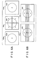
- Fig. 6A shows a plane pattern of a photodiode PD used as a sensor for obtaining an RF signal, a tracking error signal, and a focus error signal in an optical pickup system.
- the photodiode PD includes a central photodiode PD 0 divided into four parts A, B, C and D in a cruciform and side photodiodes PD S1 and PD S2 disposed on both the sides of the central photodiode PD 0 .
- Such a photodiode PD is irradiated with light from an optical recording medium, typical, an optical disk in such a manner that a central light spot SP 0 is formed on the central photodiode PD 0 , and side spots SP S1 and SP S2 are formed on the side photodiodes PD S1 and PD S2 , respectively.
- the focus error signal is obtained by calculating an equation of (A + C) - (B + D)
- the tracking error signal is obtained by calculating an equation of (E - F)
- the signal readout signal that is, RF signal is obtained by calculating an equation ( A + B + C + D ).
- Fig. 6B shows another example of a photodiode PD applied to an optical pickup system.
- the photodiode PD includes a photodiode PD 1 divided in parallel into four parts A, B, C and D in which the center side divided parts B and C are each formed into an extremely thin stripe pattern with a pitch of 14 ⁇ m, and a photodiode PD 2 divided in parallel into four parts A', B', C' and D' in which the center side divided parts B' and C' are each formed into an extremely thin stripe pattern with a pitch of 14 ⁇ m.
- Such a photodiode PD is irradiated with light in such a manner that a light spot SP 1 is formed on the photodiode PD 1 and a light spot SP 2 is formed on the photodiode PD 2 .
- the focus error signal is obtained by calculating an equation [(B + C) - (A + D)] - [(B' + C') - (A' + D')] ;
- the tracking error signal is obtained by calculating an equation of (A + B + C' + D') - (C + D + A' + B') ;
- the RF signal is obtained by calculating an equation of (A + B
- a semiconductor device having a photodiode divided into a plurality of parts, for example, the above-described photodiode PD divided into four parts has a configuration shown in Fig. 7.
- Fig. 7 is a sectional view of an essential portion of the photodiode. As shown in this figure, a cathode region 9 is divided into two parts over the entire thickness by a division region 30 and a buried isolation region 9 formed under the division region 30.
- the cathode region 9 in a non-operated state in which no reverse bias voltage is applied to the photodiode PD, the cathode region 9 is perfectly divided into two parts by the division region 30 and the buried isolation region 6 formed under the division region 30. That is to say, the p-n junction J between the anode region 4 and the cathode region 9 is divided into a plurality of junctions Jn by a plurality of the division regions 30 and the buried isolation regions 6.
- the extension of the depletion layer from each of the divided p-n junctions Jn to the anode region 4 side is shallower than the buried isolation region 6, and therefore, the depletion layer is divided into two parts by the buried region 6.
- the frequency characteristic of the photodiode is degraded for the following reason:
- the frequency characteristic of the photodiode is mainly determined by a CR time constant depending on a parasitic capacitance (C) and a parasitic resistance (R), a time required for carriers to migrate in a depletion layer of the photodiode, and a time required for carriers to diffuse in a non-depleted semiconductor layer.
- the frequency characteristic differs between a portion near the division region 30 and the buried isolation region 6, and a position sufficiently apart therefrom.
- Minority carriers that is, electrons "e” generated in the buried isolation region 6 and a portion, near the region 6, of the anode region 4 by light irradiation receive, from the region 6, forces in the direction in which the electrons "e” are separated from the region 6 as shown by an arrow "b" because the potential of the region 6 acts as a barrier against the electrons "e", minority carriers.
- the electrons "e” generated in the buried isolation region 6 and a portion, near the region 6, of the anode region 4 migrate toward the depletion layer not along a straight line but along a curved line.
- electrons "e” generated in a portion sufficiently apart from the buried isolation region 6 are not affected or little affected by the potential of the region 6, and therefore, they migrate to the depletion layer along a straight line as shown an arrow "c". That is to say, electrons generated in the buried isolation region 6 and its neighborhood are longer than electrons generated at a portion sufficiently apart from the region 6 in terms of migration distance to the depletion layer, that is, diffusion time of carriers. As a result, the frequency characteristic of the buried isolation region 6 and its neighborhood is degraded.
- the ratio of the area of the isolation regions to the light irradiation area becomes large, thereby causing a problem associated with the frequency characteristic.
- the RF signal is obtained by adding signals outputted from the divided parts of the photodiode including the regions 6, it is affected by the degradation of the frequency characteristic at the regions 6.
- the RF signal most required to ensure a high speed performance is seriously affected by the degradation of the frequency characteristic at the regions 6.
- the light receiving sensitivity of a photodiode is determined by a ratio of those, reaching a depletion layer, without generation of recombination, of carriers (electron-positive hole pairs) generated by photoelectric conversion.
- the light receiving sensitivity at the isolation portion of a photodiode will be examined.
- incident light at the isolation portion of the photodiode enters the division region 30, buried isolation region 6, and anode regions 4, 3 and 2.
- the division region 30 and the buried isolation region 6, which are positioned near the surface of the semiconductor substrate and thereby have a large light absorption, since the impurity concentration is high, the diffusion lengths of carriers generated in the vicinity of the regions 30 and 6 are short, so that there is a large possibility that the carriers be lost by recombination before reaching the depletion layer.
- the carriers generated in the anode regions 4, 3 and 2 are longer in migration distance to the depletion layer as described above, there is a large possibility that the carriers be lost by recombination during migration.
- the light receiving sensitivity is degraded at the isolation portion of the photodiode.
- An object of the present invention is to provide a photodetector, typically, a photodiode capable of improving the frequency characteristic even if the photodetector is configured such that a division portion and its neighborhood is irradiated with light.
- Another object of the present invention is to provide a photodetector, typically, a photodiode capable of improving the light receiving sensitivity even if the photodetector is configured such that a division portion and its neighborhood is irradiated with light.
- a semiconductor device including a photodetector having a junction at which a first conductive type first semiconductor portion and a second conductive type second semiconductor portion are joined to each other, the photodetector being formed on a semiconductor substrate.
- division regions are formed in part of the first semiconductor portion in such a manner as to cross the first semiconductor portion and partially enter the second semiconductor portion, so that the junction is divided into a plurality of parts by the division regions, to form a plurality of photodetector regions having the divided junction parts; and when a reverse bias voltage, which is equal to or less than a specific reverse bias voltage applied to the divided junction parts upon operation of the photodetector, is applied to the divided junction parts, depletion layers originated from two divided junction parts, disposed on both the sides of each of the division regions, of the plurality of divided junction parts extend, in the second semiconductor portion, under the division region to be brought into contact with each other.
- the adjacent depletion layers via each division region extend under the division region to be brought into contact with each other, and accordingly, it is possible to avoid the occurrence of such a potential barrier of the division region as to cause the roundabout of carriers generated under the depletion layer by light irradiation, and hence to avoid the degradation of the frequency characteristic due to the roundabout of the carriers.
- an optical pickup system including: a semiconductor light emitting device; a photodetector having a junction at which a first conductive first type semiconductor portion and a second conductive second type semiconductor portion are joined to each other, said photodetector being formed on a semiconductor substrate; and an optical system.
- division regions are formed in part of said first semiconductor portion in such a manner as to cross said first semiconductor portion and partially enter said second semiconductor portion, so that said junction is divided into a plurality of parts by said division regions, to form a plurality of photodetector regions having said divided junction parts; and when a reverse bias voltage, which is equal to or less than a specific reverse bias voltage applied to said divided junction parts upon operation of said photodetector, is applied to said divided junction parts, depletion layers originated from two divided junction parts, disposed on both the sides of each of the division regions, of said plurality of divided junction parts extend, in said second semiconductor portion, under said division region to be brought into contact with each other.
- the semiconductor device since the semiconductor device is so configured as described above, it is possible to realize a good frequency characteristic and a good light receiving sensitivity even if an area including isolation regions for isolating a plurality of divided photodiode parts from each other is irradiated with light to obtain an RF signal requiring a high speed performance, or a very thin stripe pattern or a thick pattern of the photodiode, typically used for a so-called laser coupler, is irradiated with light.
- the semiconductor device can be fabricated by the steps, the number of which is substantially the same as that of the steps of the prior art fabrication method, and accordingly, the optical pickup system using the semiconductor device can be fabricated by the steps, the number of which is substantially the same as that of the steps of the prior art fabrication method.
- Fig. 1 is a schematic sectional view of an embodiment of a semiconductor device of the present invention.
- a photodiode PD as a photodetector having a p-n junction J between a first conductive type first semiconductor portion 9 and a second conductive type second semiconductor portion 4 is formed in a semiconductor substrate 1.
- Division regions 40 (only one region 40 is shown in Fig. 1) are formed in the first semiconductor portion 9 at selected positions in such a manner as to cross the first semiconductor portion 9.
- the junction J is divided by the division regions 40 into a plurality of junction parts Jn, and simultaneously a photodetector region is divided by the junction parts Jn into a plurality of photodetector regions.
- the photodiode PD as the photodetector in this embodiment is configured as follows: namely, when a reverse bias voltage in a range of 0.3 V to 11.0 V, typically, in a range of 0.5 V to 2.5 V, which is equal to or less than that applied to the junction parts Jn upon operation of the photodiode, is applied to the junction parts Jn, as shown in Fig. 2 (which is a schematic sectional view of an essential portion of the photodiode PD), depletion layers originated from the divided junction parts Jn on both the sides of each of the division regions 40 extend, in the second semiconductor portion 4, under the division region 40 to be brought into contact with each other. In this way, as shown in Fig.
- the depletion layers shown by a chain line "a”, which are continuos to each other with part of the division region 40 put therebetween, are formed.
- a depletion layer shown by a chain line "a'”, which extends from a junction "j" between each division region 40 and the first semiconductor layer 9, is also formed.
- a high impurity concentration third semiconductor portion 18 having the same conductive type as that of the first semiconductor portion 9 is formed on the surface of each of portions, isolated from each other by the depletion layers, of the first semiconductor portion 9.
- the thickness of the third semiconductor portion 18 is set in a range of 0.01 ⁇ m to 0.2 ⁇ m.
- a fourth semiconductor portion 3 having an impurity concentration higher than that of the second semiconductor portion 4 is formed on the side, opposite to the junction J constituting the photodetector, of the second semiconductor portion 4 in such a manner as to be in contact with the second semiconductor portion 4.
- the distance between the surface of the semiconductor substrate 1 and the fourth semiconductor portion 3 is selected to be larger than the absorption wavelength of light incident on the photodetector.
- the semiconductor device shown in Fig. 1 is configured as a bipolar IC, used as a photo-IC, in which an npn type transistor TR and the anode common type photodiode PD are formed on the same semiconductor substrate 1.
- the photodiode PD is generally divided into a plurality of parts as shown in Fig. 6A or 6B; however, the photodiode PD shown in Fig. 1 is divided into two parts for an easy understanding.
- the semiconductor device in this embodiment is fabricated as follows:
- a high impurity concentration p-type buried layer 3 equivalent to the above-described fourth semiconductor portion is formed overall on one principal plane of a p-type Si semiconductor base substrate 2.
- a low impurity concentration p-type first semiconductor layer 31 for forming the anode region 4 of the photodiode, which is equivalent to the above-described second semiconductor portion is formed on the buried layer 3 by epitaxial growth.
- a high impurity concentration collector buried region 5 is formed in a transistor TR formation portion of the first semiconductor layer 31. Then, high impurity concentration buried isolation regions 6 are formed between respective circuit elements.
- the buried region 6 is not provided at each division portion of the photodiode PD unlike the prior structure shown in Figs. 5 and 7.
- a high impurity concentration p-type buried region 8 is formed in a portion at which an anode electrode 7 of the photodiode PD is to be formed.
- a cathode region 9 of the photodiode PD, equivalent to the above-described first semiconductor portion, and a low impurity concentration n-type second semiconductor layer 32 for forming a collector region 10 of the transistor TR are formed on the first semiconductor layer 31.
- the first and second semiconductor layers 31 and 32 are formed on the semiconductor base substrate 2 by expitaxial growth, to form an Si semiconductor substrate 1.
- insulating isolation layers 11 made from SiO 2 are formed, by LOCOS, are formed on the surface of the semiconductor substrate 1, that is, on the second semiconductor layer 32 in order to electrically isolate semiconductor circuit elements or regions from each other.
- a high impurity concentration p-type isolation region 12 is formed in the second semiconductor layer 32 at a position between each of the insulating isolation layers 11 provided between circuit elements and the buried isolation region 6 provided below the layer 11.
- a high impurity concentration p-type anode electrode extraction region 13 is formed on the high impurity concentration buried region 8 under the anode electrode 7 formation portion, and a high impurity concentration anode contact region 14 is formed thereon.
- a p-type division region having an impurity concentration higher than that of the cathode region 9 (equivalent to the first semiconductor portion) is formed at each division position in the photodiode PD formation portion.
- the planar pattern of the division region 40 is taken as a cruciform pattern, if the photodiode PD is configured as the photodiode PD 0 shown in Fig. 6A, or is taken as a three parallel stripe pattern, if the photodiode PD is configured as the photodiode PD 1 or PD 2 shown in Fig. 6B.
- the division region 40 is, as shown in Fig. 1, formed in such a manner as to cross the anode region 4 and partially enter the cathode region 9, thereby dividing the p-n junction J into parts.
- n-type collector electrode extraction region 15 and a p-type base region 16 are formed in the collector region 10, and an n-type emitter region 17 is formed on a base region 16.
- a cathode electrode 19 is brought into ohmic-contact with each cathode region 18.
- An insulating layer 21 made from SiO 2 is deposited on the surface of the semiconductor substrate 1, and electrode contact windows are formed in the insulating layer 21.
- An emitter electrode 20E, a base electrode 20B, and a collector electrode 20C of the transistor TR are brought into contact with the regions 15, 16, and 17 through the electrode contact windows, respectively, and an interlayer insulating layer 22 made from SiO 2 is formed thereon.
- the photodiode PD is irradiated with a light ray to be detected through the light receiving window of the light shading layer 23.
- the insulating layers 21 and 22 act as a reflection preventive film.
- the photodiode PD having the above configuration, a specific reverse bias voltage is applied between the anode electrode 14 and the cathode electrode 19 upon operation of the photodiode PD, and according to the present invention, the photodiode PD is configured as follows: namely, under a reverse bias voltage equal to or less than the above specific reverse bias voltage, as shown in Fig. 2, depletion layers (shown by the chain line "a") originated from the divided p-n junction parts Jn disposed between the cathode region 9 and the abode region 4 and on both the sides of each division region 40 extend under the division region 40 to be brought into contact with each other.
- the depth of the division region 40 is selected such that, in the state in which the reverse bias voltage is applied, the depletion layers originated from the divided p-n junction parts Jn disposed on both the sides of the division region 40 extend under the division region 40 to be brought into contact with each other.
- a p-n junction "j" (shown by the chain line “a'") between the division region 40 and the cathode region 9, and a depletion layer 41 (shown by the chain line “a") extending from the division p-n junction parts Jn disposed between the cathode region 9 and the anode region 4 and on both the sides of the division region 40 are formed at each division portion of the cathode region 9, that is, the first semiconductor portion.
- the cathode region (first semiconductor portion) 9 is specified such that the thickness is in a range of 0.01 to 10 ⁇ m and the impurity concentration is in a range of 1 ⁇ 10 11 to 1 ⁇ 10 16 atoms/cm 3 .
- the anode region (second semiconductor portion) 4 is specified such that the thickness is in a range of 0.01 to 600 ⁇ m and the impurity concentration is in a range of 1 ⁇ 10 11 to 1 ⁇ 10 16 atoms/cm 3 .
- the high impurity concentration region (third semiconductor portion) 18 is specified such that the thickness is in a range of 0.01 to 0.2 ⁇ m and the impurity concentration is in a range of 1 ⁇ 10 15 to 1 ⁇ 10 21 atoms/cm 3 .
- the buried layer (fourth semiconductor portion) 3 is specified such that the thickness is in a range of 1 to 30 ⁇ m and the impurity concentration is in a range of 1 ⁇ 10 16 to 1 ⁇ 10 21 atoms/cm 3 .
- the buried isolation layer 6 is specified such that the thickness is in a range of 0.01 to 10 ⁇ m and the impurity concentration is in a range of 1 ⁇ 10 14 to 1 ⁇ 10 21 atoms/cm 3 .
- the impurity concentration of the second semiconductor portion is set in a range of 2 ⁇ 10 14 atoms/cm 3 or less in order that the depletion layer 41 can perfectly deplete the anode region 4 (second semiconductor portion), that is, can reach up to the buried layer 3 (fourth semiconductor portion), and it may be more desirable that the impurity concentration is set in a range of 5 ⁇ 10 14 atoms/cm 3 or less in order that the depletion layer 41 can deplete the cathode region 9 (first semiconductor portion).
- the distance between the surface of the semiconductor substrate 1 and the fourth semiconductor portion 3 is selected to be larger than the absorption wavelength of light incident on the photodetector.
- the depletion layer 41 extending under the high impurity concentration division region 40 is formed upon operation of the photodetector of the semiconductor device, minority carriers, that is, electrons in this embodiment generated by light irradiation in the anode region 4 (second semiconductor portion) can reach the depletion layer 41 with their migration lengths kept nearly constant, as shown by arrows "b" and "c" designating migration routes in Fig. 2, that is, without being curved by the potential due to the presence of the division region 40 or isolation region, with a result that the frequency characteristic of the photodetector can be improved.
- the depletion layer 41 extends around the underside of the high impurity concentration division (isolation) region 40, minority carriers generated in the anode region (second semiconductor portion) 4 by light irradiation can reach the depletion layer while keeping nearly constant the migration lengths to the depletion layer irrespective of the presence or absence of the isolation portion, with a result that the light receiving sensitivity at the isolation portion is not degraded even if the isolation portion has a wide width.
- the photodetector that is, the photodiode PD configured such that an area including each division portion is irradiated with light
- the depth of the division region 40 is set at such a value as for the region 40 to cross the first semiconductor portion 9.
- the cross-section of the division region 40 can be reduced. This means that the diffusion lengths of the minority carriers at a high concentration to the division region 40 become short. Accordingly, it is possible to reduce the quantity of light absorbed by the division region 40, and hence to improve the sensitivity.
- the semiconductor device in this embodiment is configured as a photo-IC in which the transistor is formed as another circuit element, together with the photodetector, that is, the photodiode, on the common semiconductor substrate 1; however, it may be configured as an IC in which a pnp type transistor, a resistance element and a capacitor configured by semiconductor regions, and the like are formed as other circuit elements, together with the photodetector, on the common semiconductor substrate 1.
- Fig. 1 only one photodiode PD divided into a plurality of parts is shown as the photodetector; however, the present invention can be applied to a photo-IC in which as shown in Figs. 6A and 6B, one divided photodiode, a non-divided photodiode, and a plurality of photodiodes composed of divided photodiodes are formed on the common semiconductor substrate 1.
- Fig. 3 is a schematic view showing the configuration of an optical pickup system of the present invention, which includes the semiconductor device having a photodetector according to the present invention.
- the optical pickup system includes a laser coupler, and an optical system 53, that is, an objective lens.
- the laser coupler integrally includes a semiconductor light emitting device, typically, a semiconductor laser 51 and a semiconductor device 52 having a photodetector according to the present invention.
- the semiconductor device 52 includes two photodiodes PD 1 and PD 2 shown in Fig. 6B. To be more specific, the semiconductor device 52 including the photodiodes PD 1 and PD 2 each having the same configuration as that of the photodiode PD shown in Fig. 1 and other circuit elements are formed on a semiconductor substrate 1.
- a micro-prism 55 is mounted on the semiconductor substrate 1 of the semiconductor device 52 at a position over the photodiodes PD 1 and PD 2 .
- a forward laser light ray L emitted from the semiconductor laser 51 is reflected from a tilt plane 55M of the micro-prism 55, to be made incident on an optical recording medium 56, typically, an optical disk through the optical system 53.
- the light ray reflected from the medium 56 is returned to the micro-prism 55, being bent by the tilt plane 55M to be introduced in the prism 55, and is made incident on one photodiode PD 1 of the semiconductor device 52.
- the light ray reflected from the photodiode PD 1 is made incident on the other photodiode PD 2 of the semiconductor device 52.
- the optical recording medium 56 has recording information pits and grooves for obtaining tracking signals, and accordingly, by calculating the above-described outputs A to D and A' to D' with respect to the return light ray having been made incident on the photodiodes PD 1 and PD 2 , the tracking error signal, focus error signal, and RF signal can be obtained.
- the positional relationship between the optical recording medium and the laser light ray emitted thereto can be controlled on the basis of the tracking error signal and the positional adjustment (focusing adjustment) of the optical system 53 is performed on the basis of the focus error signal, in accordance with a known control process (not shown).
- a rearward laser light ray emitted from the semiconductor laser 51 is made incident on the monitor photodetector 54, to detect the output of the rearward laser light ray equivalent to the forward laser light rays L, thereby setting the output at a specific value by controlling a drive voltage applied to the laser 51.
- the optical pickup system having the above configuration allows not only accurate tracking and focusing, but also obtainment of the RF signal having a high S/N ratio because the photodetector, that is, photodiode has excellent frequency characteristic and light receiving sensitivity.
- a first conductive type (for example, p-type) Si semiconductor base substrate 2 is prepared. While not shown, an oxide film having a thickness of about 120 nm is formed on the surface of the semiconductor base substrate 2 by thermal oxidation, and boron ions (B + ) are implanted at an implantation energy of 30 keV in a dose of 2.5 ⁇ 10 15 /cm 2 overall in one principal plane of the semiconductor base substrate 2 through the oxide film.
- B + boron ions
- the base substrate 2 is annealed in an N 2 atmosphere kept at 1200°C for 80 min for activating boron ions thus implanted.
- the base substrate 2 is further heat-treated in a so-called wet O 2 atmosphere kept at 1200°C for 20 min in order to remove defects caused by damage upon ion implantation, to form a p-type buried layer 3.
- the oxide film is then removed by using hydrofluoric acid.
- a first semiconductor layer 31 having the same conductive type (p-type) as that of the buried layer 3 is formed by epitaxial growth on the principal plane of the semiconductor base substrate 2, that is, on the buried layer 3 to a thickness of 20 ⁇ m.
- the resistivity of the first semiconductor layer 31 is set at 50 ⁇ cm.
- the surface of the first semiconductor layer 31 is subjected to thermal oxidation, to form an oxide film having a thickness of 120 nm, and the surface of the oxide film is coated with a photoresist, followed by pattern exposure and development, to form a photoresist film having a specific pattern.
- the oxide film formed on the surface of the first semiconductor layer 31 is etched by using the photoresist film as a mask, to form openings in the oxide film.
- the photoresist film is then removed by using a mixed solution of hydrogen peroxide and H 2 SO 4 .
- Boron ions (B + ) are implanted at an implantation energy of 30 keV in a dose of 2.5 ⁇ 10 15 /cm 2 in the first semiconductor layer 31 at the periphery of a photodiode formation portion and at portions for isolation between circuit elements through the above openings.
- the base semiconductor 2 is annealed in an N 2 atmosphere kept at 1200°C for 80 min for activating boron ions thus implanted.
- the base substrate 2 is further subjected to oxidation in a so-called wet O 2 atmosphere kept at 1200°C for 20 min in order to remove defects caused by damage upon ion implantation, to form p-type buried isolation regions 6 and a high impurity concentration buried region 8 for extraction of an electrode of an anode region of the photodiode.
- a photoresist film of a specific pattern having an opening at a position equivalent to a transistor formation portion is formed on the first semiconductor layer 31.
- the oxide film formed on the surface of the first semiconductor layer 31 is etched by using the photoresist film as a mask, to form an opening in the oxide film.
- the photoresist film is then removed by using a mixed solution of hydrogen peroxide and sulfuric acid.
- a second conductive type (n-type in this embodiment) collector buried region 5 is formed in the first semiconductor layer 31 through the opening formed in the oxide film by thermal diffusion using Sb 2 O 3 as a solid source at 1200°C for 60 min.
- the oxide film is then removed by heat-treatment using hydrofluoric acid.
- a second conductive type that is, n-type second semiconductor layer 32 (thickness: 1.6 ⁇ m, resistivity: 1 ⁇ cm) is formed by epitaxial growth on the first semiconductor layer 31, to form a semiconductor substrate 1.
- the impurities contained in the high impurity concentration collector buried region 5, high impurity concentration buried isolation regions 6, and high impurity concentration buried region 8 formed in the first semiconductor layer 31 are diffused in the second semiconductor layer 32, whereby the regions 5, 6 and 8 enter the second semiconductor layer 32.
- Insulating isolation layers 11 are formed by LOCOS as follows: namely, the surface of the second semiconductor layer 32 is subjected to thermal oxidation, to form an oxide film made from SiO 2 having a thickness of 20 nm, and a silicon nitride (SiO x N y ) film having a thickness of 65 nm is deposited on the oxide film by a low pressure CVD process; the oxide film, nitride film and the second semiconductor layer 32 are selectively etched by RIE (reactive Ion Etching) to a thickness of about 400 nm; and the second semiconductor layer 32 is subjected to wet O 2 atmosphere kept at 1050°C by using the remaining nitride film as an anti-oxidation mask, to form the insulating isolating layers 11 having a thickness of 800 nm.
- RIE reactive Ion Etching
- the nitride film is selectively etched at 150°C by using phosphoric acid, and a high impurity concentration collector electrode extraction region 15 of the first conductive type, that is, n-type is formed on part of the collector buried region 5 of the second semiconductor layer 32 by implanting phosphorus ions (P + ) at 70 keV in a dose of 1 ⁇ 10 16 /cm 2 .
- the resultant substrate is heat-treated in an N 2 atmosphere kept at 1050°C for 60 min for activating the impurity.
- a high impurity p-type isolation region 12, an anode electrode extraction region 13, a division region 40, and a high impurity concentration n-type anode region 18 are formed as follows:
- the isolation region 12 and the anode electrode extraction region 13 are formed by selectively implanting boron ions (B + ) at 500 key in a dose of 1 ⁇ 10 14 /cm 2 .
- the high concentration cathode region 18 is formed by implanting arsenic ions (As + ) at 70 keV in a dose of 1 ⁇ 10 15 /cm 2 .
- the resultant substrate is heat-treated at 1000°C for 30 min for activating the impurities, to form the high impurity concentration p-type isolation region 12, anode electrode extraction region 13, division region 40, and high impurity concentration n-type cathode region 18.
- the high impurity p-type isolation region 12, anode electrode extraction region 13, and division region 40 are simultaneously formed.
- the isolation region 12 and the anode electrode extraction region 13 can be formed in such a manner as to be in contact with the buried isolation region 6 and the high impurity concentration buried region 8, respectively.
- the division region 40 is, as described above, formed in such a manner as to cross the cathode region 9 formed by the second semiconductor layer 32 and slightly enter the first semiconductor layer 31.
- the subsequent steps may be performed in accordance with a general process of fabricating a bipolar transistor IC as follows:
- An insulating under layer such as an oxide film is formed on the surface of the second semiconductor layer 32 of the semiconductor substrate 1, and an opening is formed at a base region formation portion of the transistor and also an opening is formed at a position over the anode electrode extraction 13, by photolithography and etching.
- a first polycrystalline semiconductor layer 61 made from poly-silicon heavily doped with a p-type impurity is formed to block the above openings.
- the polycrystalline semiconductor layer 61 is removed, by photolithography and etching, except for the base region formation portion and its electrode extraction portion of the transistor and the anode electrode extraction region 13 and its electrode extraction portion of the photodiode.
- An opening is formed in the base region formation portion of the first polycrystalline semiconductor layer 61 at an intrinsic base region 16i formation portion, and an intrinsic base region 16i is formed by diffusing the p-type impurity through the opening. Then, an insulating layer made from SiO 2 is formed, to form a surface insulating layer 21 having a specific thickness, together with the insulating under layer previously formed. An opening is formed in the insulating layer 21 at the position corresponding to the intrinsic base region 16i, and a second polycrystalline semiconductor layer 62 made from poly-silicon heavily doped with an n-type impurity is formed to block the opening.
- the second polycrystalline semiconductor layer 62 is removed, by photolithography and etching, except for an emitter electrode extraction region.
- a high impurity concentration p-type graft base region 16g is formed around the intrinsic base region 16i, a high impurity concentration anode contact region 14 is formed on the anode electrode extraction region 13, and a high impurity concentration n-type emitter region 17 is formed on the intrinsic base region 16i by diffusing the impurities from the first and second polycrystalline semiconductor layers 61 and 62 to the semiconductor layer 32.
- Electrode contact windows are formed in the insulating layer 21.
- An emitter electrode 20E, a base electrode 20B, and a collector electrode 20C of the transistor TR are brought into contact with the regions 15, 16, and 17 through the electrode contact windows, respectively, and an interlayer insulating layer 22 made from SiO 2 is formed thereon.
- a light shading layer 23 made from Al, which has a light receiving window, is formed on the interlayer insulating layer 22, and a protective layer 24 is formed thereon.
- the photodiode PD is irradiated with a light ray to be detected through the light receiving window of the light shading layer 23.
- the insulating layers 21 and 22 act as a reflection preventive film.
- the photodiode PD is divided into a plurality of parts by the depletion layers originated from the junctions j and the depletion layers originated from the p-n junction parts J divided from the junction J constituting the photodiode PD by the division regions 40.
- the isolation portion of the photodiode PD does not have the buried isolation region 6 of the prior art structure shown in Fig. 7.
- the bipolar transistor TR has a so-called double poly-silicon structure using the first and second polycrystalline semiconductor layers 61 and 62; however, the double poly-silicon structure may be formed by ion implantation, or may be displaced with a so-called single poly-silicon emitter structure in which the emitter region is formed by ion implantation.
- the formation of the division region 40 is made simultaneously with the formation of the isolation region 12 in the above embodiment; however, it may be made separately from the formation of the isolation region 12.
- the second semiconductor portion (anode region 4 in the above embodiment) is formed by epitaxial growth in the above embodiment; however, it may be formed by the semiconductor base substrate 2 itself.
- the first conductive type is taken as n-type and the second conductive type is taken as p-type, that is, the photodiode is configured as the anode common type in which the cathode is disposed on the light receiving surface side; however, the conductive type may be reversed to that described above.
- the description of the semiconductor device having a photodetector, the fabrication method thereof, and the optical pickup system using the semiconductor device in the above embodiment is for illustrative purposes only, and it is to be understood that changes and variations may be made without departing from the spirit or scope of the following claims.
Abstract
A semiconductor device includes a photodetector having a
junction at which a first conductive type first
semiconductor portion and a second conductive type second
semiconductor portion are joined to each other. In this
photodetector, division regions are formed in part of the
first semiconductor portion in such a manner as to cross
the first semiconductor portion and partially enter the
second semiconductor portion, so that the junction is
divided into a plurality of parts by the division regions,
to form a plurality of photodetector regions having the
divided junction parts. When a reverse bias voltage,
which is equal to or less than a specific reverse bias
voltage applied to the divided junction parts upon
operation of the photodetector, is applied to the divided
junction parts, depletion layers originated from two
divided junction parts, disposed on both the sides of
each of the division regions, of the plurality of divided
junction parts extend, in the second semiconductor
portion, under the division region to be brought into
contact with each other. With this configuration, the
frequency characteristic and the light receiving
sensitivity of the photodetector are improved.
Description
- The present invention relates to a semiconductor device having a photodetector and an optical pickup system using the semiconductor device.
- A photodiode as a photodetector capable of converting a light signal into an electric signal has been extensively used for optical sensors for controlling various kinds of photoelectric converters, for example, an optical sensor for obtaining a recording information signal (hereinafter, referred to as "RF signal"), a tracking error signal, a focusing error signal, and the like in a so-called optical pickup system for recording and/or reproducing light signals on and/or from an optical recording medium.
- A photodetector is formed, together with various circuit elements such as a bipolar transistor, resistance, and capacitor, on a common semiconductor substrate, to be thus configured as a so-called photo-IC (Integrated Circuit). Such a photo-IC is generally fabricated in accordance with a method of fabricating a bipolar transistor as one of the above-described circuit elements.
- As a photo-IC having a fast, high-sensitive photodetector, there has been proposed a photo-IC including a high resistance expitaxial semiconductor layer.
- Fig. 5 is a schematic sectional view showing a prior art photo-IC on which a photodiode PD as a photodetector and a bipolar transistor TR are mixedly formed. The photo-IC shown in Fig. 5 has a configuration of a bipolar IC on which an npn type transistor TR and an anode common type photodiode PD are formed on the same semiconductor substrate 1.
- The method of fabricating the bipolar IC will be described below. A high impurity concentration p-type buried
layer 3 is formed on the entire principal plane of a p-type Sisemiconductor base substrate 2, and a low impurity concentration p-typefirst semiconductor layer 31 for forming ananode region 4 of the photodiode PD is formed on the buriedlayer 3 by epitaxial growth. A high impurity concentration collector buriedregion 5 is formed on a transistor TR formation area of thefirst semiconductor layer 31. High impurity concentration buriedisolation regions 6 are selectively formed in order to isolate circuit elements from each other and to divide the photodiode PD into parts (as will be described below). A high impurity concentration p-type buriedregion 8 is formed, simultaneously with the formation of the buriedisolation regions 6, under a contact of ananode electrode 7 of the photodetector PD. - A low impurity concentration n-type
second semiconductor layer 32 for forming acathode region 9 of the photodiode PD and acollector region 10 of the transistor TR is formed on thefirst semiconductor layer 31 by epitaxial growth. - In this way, the first and
second semiconductor layers semiconductor base substrate 2 by epitaxial growth, to form an Si semiconductor substrate 1. Insulatingisolation layers 11 made from SiO2 are formed, by a so-called LOCOS (Local Oxidation of Silicon), on the surface of the Si semiconductor substrate 1, that is, on thesecond semiconductor layer 31 in order to electrically isolate semiconductor circuits elements or regions from each other. - In the
second semiconductor layer 32, a high impurity concentration p-type isolation region 12 is formed between theinsulating isolation layer 11 and the buriedisolation region 6 positioned thereunder at each insulating isolation portion between adjacent circuit elements. A high impurity concentration p-type anodeelectrode extraction region 13 is formed on the high impurity concentration buriedregion 8, and a high impurity concentrationanode contact region 14 is formed on the anodeelectrode extraction region 13. A high impurity concentration p-type division region 30 is formed on the buriedregion 6, which is formed at the division region for dividing theanode region 4 into two parts, in such a manner as to be in contact with theregion 6. - A high impurity concentration n-type collector
electrode extraction region 15 and a p-type base region 16 are formed in thecollector region 10. An n-type emitter region 17 is formed on thebase region 16. - A high impurity
concentration cathode region 18 is formed on eachcathode region 9 of the photodiode PD, and acathode electrode 19 is in ohmic-contact with thecathode region 18. - An insulating
layer 21 made from SiO2 is deposited on the surface of the semiconductor substrate 1, and electrode contact windows are formed in the insulatinglayer 21. Anemitter electrode 20E, abase electrode 20B, and acollector electrode 20C of the transistor TR are brought into contact with theregions interlayer insulating layer 22 made from SiO2 is formed thereon. Alight shading layer 23 made from Al, which has a light receiving window, is formed on theinterlayer insulating layer 22, and aprotective layer 24 is formed thereon. - The photodiode PD is irradiated with a light ray to be detected through the light receiving window of the
light shading layer 23. In this case, theinsulating layers - The photodiode PD configured as the bipolar IC thus fabricated is used as a sensor for obtaining an RF signal, a tracking error signal, and a focus error signal in an optical pickup system for recording and/or reproducing light signals on and/or from an optical recording medium.
- Fig. 6A shows a plane pattern of a photodiode PD used as a sensor for obtaining an RF signal, a tracking error signal, and a focus error signal in an optical pickup system. In this example, the photodiode PD includes a central photodiode PD0 divided into four parts A, B, C and D in a cruciform and side photodiodes PDS1 and PDS2 disposed on both the sides of the central photodiode PD0. Such a photodiode PD is irradiated with light from an optical recording medium, typical, an optical disk in such a manner that a central light spot SP0 is formed on the central photodiode PD0, and side spots SPS1 and SPS2 are formed on the side photodiodes PDS1 and PDS2, respectively. In this case, assuming that the outputs obtained by photoelectric conversion at the four divided parts A, B, C and D of the central photodiode PD0 are taken as outputs A, B, C and D, the focus error signal is obtained by calculating an equation of
- Fig. 6B shows another example of a photodiode PD applied to an optical pickup system. In this example, the photodiode PD includes a photodiode PD1 divided in parallel into four parts A, B, C and D in which the center side divided parts B and C are each formed into an extremely thin stripe pattern with a pitch of 14 µm, and a photodiode PD2 divided in parallel into four parts A', B', C' and D' in which the center side divided parts B' and C' are each formed into an extremely thin stripe pattern with a pitch of 14 µm. Such a photodiode PD is irradiated with light in such a manner that a light spot SP1 is formed on the photodiode PD1 and a light spot SP2 is formed on the photodiode PD2. In this case, assuming that the outputs from the divided parts A, B, C and D of the photodiode PD1 are taken as outputs A, B, C, and D and the outputs from the divided parts A', B', C' and D' of the photodiode PD2 are taken as outputs A', B', C' and D', the focus error signal is obtained by calculating an equation
- A semiconductor device having a photodiode divided into a plurality of parts, for example, the above-described photodiode PD divided into four parts has a configuration shown in Fig. 7. Fig. 7 is a sectional view of an essential portion of the photodiode. As shown in this figure, a
cathode region 9 is divided into two parts over the entire thickness by adivision region 30 and a buriedisolation region 9 formed under thedivision region 30. - According to the above-described prior art configuration, in a non-operated state in which no reverse bias voltage is applied to the photodiode PD, the
cathode region 9 is perfectly divided into two parts by thedivision region 30 and the buriedisolation region 6 formed under thedivision region 30. That is to say, the p-n junction J between theanode region 4 and thecathode region 9 is divided into a plurality of junctions Jn by a plurality of thedivision regions 30 and the buriedisolation regions 6. When a reverse bias voltage is applied to the photodiode PD for operating the photodiode PD, depletion layers are extended from each of the divided p-n junctions Jn and from each of the p-n junctions j between thedivision layers 30 andcathode region 9. In Fig. 7, chain lines "a" and "a'" each designate the extension of the depletion layer. It should be noted that in Fig. 7, parts corresponding to those shown in Fig. 5 are designated by the same characters and the overlapped explanation thereof is omitted. - As shown in Fig. 7, the extension of the depletion layer from each of the divided p-n junctions Jn to the
anode region 4 side is shallower than the buriedisolation region 6, and therefore, the depletion layer is divided into two parts by the buriedregion 6. - In the case of the semiconductor device including a photodiode having a configuration shown in Figs. 6A or 6B, that is, so-called photo-IC, in which light spots are formed on the divided parts A, B, C and D or A', B', C' and D', that is, on each
division region 30 and the buriedisolation region 6 formed thereunder, the frequency characteristic of the photodiode is degraded for the following reason: - The frequency characteristic of the photodiode is mainly determined by a CR time constant depending on a parasitic capacitance (C) and a parasitic resistance (R), a time required for carriers to migrate in a depletion layer of the photodiode, and a time required for carriers to diffuse in a non-depleted semiconductor layer.
- Accordingly, in the above-described photodiode PD divided into four parts, the frequency characteristic differs between a portion near the
division region 30 and the buriedisolation region 6, and a position sufficiently apart therefrom. - This will be more fully described with reference to Fig. 7. Minority carriers, that is, electrons "e" generated in the buried
isolation region 6 and a portion, near theregion 6, of theanode region 4 by light irradiation receive, from theregion 6, forces in the direction in which the electrons "e" are separated from theregion 6 as shown by an arrow "b" because the potential of theregion 6 acts as a barrier against the electrons "e", minority carriers. As a result, the electrons "e" generated in the buriedisolation region 6 and a portion, near theregion 6, of theanode region 4 migrate toward the depletion layer not along a straight line but along a curved line. On the contrary, electrons "e" generated in a portion sufficiently apart from the buriedisolation region 6 are not affected or little affected by the potential of theregion 6, and therefore, they migrate to the depletion layer along a straight line as shown an arrow "c". That is to say, electrons generated in the buriedisolation region 6 and its neighborhood are longer than electrons generated at a portion sufficiently apart from theregion 6 in terms of migration distance to the depletion layer, that is, diffusion time of carriers. As a result, the frequency characteristic of the buriedisolation region 6 and its neighborhood is degraded. - Accordingly, in the case of the above-described photodiode divided into four parts, when a light spot is formed on an area including the isolation regions between the four divided parts, that is, the buried
isolation regions 6, the ratio of the area of the isolation regions to the light irradiation area becomes large, thereby causing a problem associated with the frequency characteristic. In particular, since the RF signal is obtained by adding signals outputted from the divided parts of the photodiode including theregions 6, it is affected by the degradation of the frequency characteristic at theregions 6. The RF signal most required to ensure a high speed performance is seriously affected by the degradation of the frequency characteristic at theregions 6. - The light receiving sensitivity of a photodiode is determined by a ratio of those, reaching a depletion layer, without generation of recombination, of carriers (electron-positive hole pairs) generated by photoelectric conversion.
- The light receiving sensitivity at the isolation portion of a photodiode will be examined. Referring to Fig. 7, incident light at the isolation portion of the photodiode enters the
division region 30, buriedisolation region 6, andanode regions division region 30 and the buriedisolation region 6, which are positioned near the surface of the semiconductor substrate and thereby have a large light absorption, since the impurity concentration is high, the diffusion lengths of carriers generated in the vicinity of theregions - The carriers generated in the
anode regions - As a result, the light receiving sensitivity is degraded at the isolation portion of the photodiode.
- Accordingly, in the case of the above-described photodiode divided into four parts, when a light spot to be detected is formed on an area including the isolation regions between the four divided parts, that is, the
division region 30 and buriedisolation regions 6, since the ratio of the vertical sectional area of the division and isolation regions to the light irradiation area becomes large and further the width of each isolation region may be sometimes wider on the basis of the design of an optical pickup, the degradation of the light receiving sensitivity in the division or isolation region causes a large problem. - An object of the present invention is to provide a photodetector, typically, a photodiode capable of improving the frequency characteristic even if the photodetector is configured such that a division portion and its neighborhood is irradiated with light.
- Another object of the present invention is to provide a photodetector, typically, a photodiode capable of improving the light receiving sensitivity even if the photodetector is configured such that a division portion and its neighborhood is irradiated with light.
- To achieve the above objects, according to a first aspect of the present invention, there is provided a semiconductor device including a photodetector having a junction at which a first conductive type first semiconductor portion and a second conductive type second semiconductor portion are joined to each other, the photodetector being formed on a semiconductor substrate. In this semiconductor device, division regions are formed in part of the first semiconductor portion in such a manner as to cross the first semiconductor portion and partially enter the second semiconductor portion, so that the junction is divided into a plurality of parts by the division regions, to form a plurality of photodetector regions having the divided junction parts; and when a reverse bias voltage, which is equal to or less than a specific reverse bias voltage applied to the divided junction parts upon operation of the photodetector, is applied to the divided junction parts, depletion layers originated from two divided junction parts, disposed on both the sides of each of the division regions, of the plurality of divided junction parts extend, in the second semiconductor portion, under the division region to be brought into contact with each other.
- With this configuration of the above semiconductor device, when a reverse bias voltage equal to or less than the specific value is applied to each of the divided p-n junction parts, the adjacent depletion layers via each division region extend under the division region to be brought into contact with each other, and accordingly, the division region between the photodetector regions becomes shallower than the prior art division region which includes the buried isolation region. As a result, the absorption wavelength of light incident on this division region is reduced, to enhance the light receiving sensitivity of the photodetector.
- Further, when a reverse bias voltage equal to or less than the specific value is applied to each of the divided p-n junction parts, the adjacent depletion layers via each division region extend under the division region to be brought into contact with each other, and accordingly, it is possible to avoid the occurrence of such a potential barrier of the division region as to cause the roundabout of carriers generated under the depletion layer by light irradiation, and hence to avoid the degradation of the frequency characteristic due to the roundabout of the carriers.
- According to a second aspect of the present invention, there is provided an optical pickup system including: a semiconductor light emitting device; a photodetector having a junction at which a first conductive first type semiconductor portion and a second conductive second type semiconductor portion are joined to each other, said photodetector being formed on a semiconductor substrate; and an optical system. In this photodetector, division regions are formed in part of said first semiconductor portion in such a manner as to cross said first semiconductor portion and partially enter said second semiconductor portion, so that said junction is divided into a plurality of parts by said division regions, to form a plurality of photodetector regions having said divided junction parts; and when a reverse bias voltage, which is equal to or less than a specific reverse bias voltage applied to said divided junction parts upon operation of said photodetector, is applied to said divided junction parts, depletion layers originated from two divided junction parts, disposed on both the sides of each of the division regions, of said plurality of divided junction parts extend, in said second semiconductor portion, under said division region to be brought into contact with each other.
- With this configuration of the optical pickup system, since the semiconductor device is so configured as described above, it is possible to realize a good frequency characteristic and a good light receiving sensitivity even if an area including isolation regions for isolating a plurality of divided photodiode parts from each other is irradiated with light to obtain an RF signal requiring a high speed performance, or a very thin stripe pattern or a thick pattern of the photodiode, typically used for a so-called laser coupler, is irradiated with light.
- According to the present invention, the semiconductor device can be fabricated by the steps, the number of which is substantially the same as that of the steps of the prior art fabrication method, and accordingly, the optical pickup system using the semiconductor device can be fabricated by the steps, the number of which is substantially the same as that of the steps of the prior art fabrication method.
-
- Fig. 1 is a schematic sectional view of an embodiment of a semiconductor device according to the present invention;
- Fig. 2 is a schematic sectional view of an essential portion of the semiconductor device shown in Fig. 1 for illustrating the operation of the semiconductor device;
- Fig. 3 is a configuration view of an embodiment of an optical pickup system according to the present invention;
- Figs. 4A and 4B are views illustrating an embodiment of a fabrication method according to the present invention;
- Fig. 5 is a schematic sectional view of a prior art semiconductor device
- Figs. 6A and 6B are diagrams each showing a pattern of a photodiode; and
- Fig. 7 is a schematic sectional view of an essential portion of the prior art semiconductor device for illustrating the operation of the semiconductor device.
-
- Hereinafter, embodiments of the present invention will be described with reference to the accompanying drawings.
- Fig. 1 is a schematic sectional view of an embodiment of a semiconductor device of the present invention.
- Referring to Fig. 1, a photodiode PD as a photodetector having a p-n junction J between a first conductive type
first semiconductor portion 9 and a second conductive typesecond semiconductor portion 4 is formed in a semiconductor substrate 1. - Division regions 40 (only one
region 40 is shown in Fig. 1) are formed in thefirst semiconductor portion 9 at selected positions in such a manner as to cross thefirst semiconductor portion 9. The junction J is divided by thedivision regions 40 into a plurality of junction parts Jn, and simultaneously a photodetector region is divided by the junction parts Jn into a plurality of photodetector regions. - The photodiode PD as the photodetector in this embodiment is configured as follows: namely, when a reverse bias voltage in a range of 0.3 V to 11.0 V, typically, in a range of 0.5 V to 2.5 V, which is equal to or less than that applied to the junction parts Jn upon operation of the photodiode, is applied to the junction parts Jn, as shown in Fig. 2 (which is a schematic sectional view of an essential portion of the photodiode PD), depletion layers originated from the divided junction parts Jn on both the sides of each of the
division regions 40 extend, in thesecond semiconductor portion 4, under thedivision region 40 to be brought into contact with each other. In this way, as shown in Fig. 2, the depletion layers shown by a chain line "a", which are continuos to each other with part of thedivision region 40 put therebetween, are formed. In addition, a depletion layer shown by a chain line "a'", which extends from a junction "j" between eachdivision region 40 and thefirst semiconductor layer 9, is also formed. - It should be noted that in Fig. 2, parts corresponding to those shown in Fig. 1 are designated by the same characters and the overlapped explanation thereof is omitted.
- Referring again to Fig. 1, a high impurity concentration
third semiconductor portion 18 having the same conductive type as that of thefirst semiconductor portion 9 is formed on the surface of each of portions, isolated from each other by the depletion layers, of thefirst semiconductor portion 9. - The thickness of the
third semiconductor portion 18 is set in a range of 0.01 µm to 0.2 µm. - A
fourth semiconductor portion 3 having an impurity concentration higher than that of thesecond semiconductor portion 4 is formed on the side, opposite to the junction J constituting the photodetector, of thesecond semiconductor portion 4 in such a manner as to be in contact with thesecond semiconductor portion 4. - In this case, the distance between the surface of the semiconductor substrate 1 and the
fourth semiconductor portion 3 is selected to be larger than the absorption wavelength of light incident on the photodetector. - The semiconductor device shown in Fig. 1 is configured as a bipolar IC, used as a photo-IC, in which an npn type transistor TR and the anode common type photodiode PD are formed on the same semiconductor substrate 1. In this bipolar IC, the photodiode PD is generally divided into a plurality of parts as shown in Fig. 6A or 6B; however, the photodiode PD shown in Fig. 1 is divided into two parts for an easy understanding.
- The semiconductor device in this embodiment is fabricated as follows:
- A high impurity concentration p-type buried
layer 3 equivalent to the above-described fourth semiconductor portion is formed overall on one principal plane of a p-type Sisemiconductor base substrate 2. A low impurity concentration p-typefirst semiconductor layer 31 for forming theanode region 4 of the photodiode, which is equivalent to the above-described second semiconductor portion is formed on the buriedlayer 3 by epitaxial growth. A high impurity concentration collector buriedregion 5 is formed in a transistor TR formation portion of thefirst semiconductor layer 31. Then, high impurity concentration buriedisolation regions 6 are formed between respective circuit elements. - It should be noted that at the above fabrication steps, as the feature of the present invention, the buried
region 6 is not provided at each division portion of the photodiode PD unlike the prior structure shown in Figs. 5 and 7. - A high impurity concentration p-type buried
region 8 is formed in a portion at which ananode electrode 7 of the photodiode PD is to be formed. - A
cathode region 9 of the photodiode PD, equivalent to the above-described first semiconductor portion, and a low impurity concentration n-typesecond semiconductor layer 32 for forming acollector region 10 of the transistor TR are formed on thefirst semiconductor layer 31. - In this way, the first and second semiconductor layers 31 and 32 are formed on the
semiconductor base substrate 2 by expitaxial growth, to form an Si semiconductor substrate 1. Then, insulating isolation layers 11 made from SiO2 are formed, by LOCOS, are formed on the surface of the semiconductor substrate 1, that is, on thesecond semiconductor layer 32 in order to electrically isolate semiconductor circuit elements or regions from each other. - A high impurity concentration p-
type isolation region 12 is formed in thesecond semiconductor layer 32 at a position between each of the insulating isolation layers 11 provided between circuit elements and the buriedisolation region 6 provided below thelayer 11. A high impurity concentration p-type anodeelectrode extraction region 13 is formed on the high impurity concentration buriedregion 8 under theanode electrode 7 formation portion, and a high impurity concentrationanode contact region 14 is formed thereon. - Next, as the feature of the semiconductor device in this embodiment, a p-type division region having an impurity concentration higher than that of the cathode region 9 (equivalent to the first semiconductor portion) is formed at each division position in the photodiode PD formation portion.
- The planar pattern of the
division region 40 is taken as a cruciform pattern, if the photodiode PD is configured as the photodiode PD0 shown in Fig. 6A, or is taken as a three parallel stripe pattern, if the photodiode PD is configured as the photodiode PD1 or PD2 shown in Fig. 6B. - The
division region 40 is, as shown in Fig. 1, formed in such a manner as to cross theanode region 4 and partially enter thecathode region 9, thereby dividing the p-n junction J into parts. - Then, a high impurity concentration n-type collector
electrode extraction region 15 and a p-type base region 16 are formed in thecollector region 10, and an n-type emitter region 17 is formed on abase region 16. - A
cathode region 18 having an impurity concentration higher than that of thecathode region 9, which is equivalent to the above-described third semiconductor portion, is formed on each of parts of thecathode region 9 divided by thedivision regions 40 of the photodiode PD. Acathode electrode 19 is brought into ohmic-contact with eachcathode region 18. - An insulating
layer 21 made from SiO2 is deposited on the surface of the semiconductor substrate 1, and electrode contact windows are formed in the insulatinglayer 21. Anemitter electrode 20E, abase electrode 20B, and acollector electrode 20C of the transistor TR are brought into contact with theregions layer 22 made from SiO2 is formed thereon. Alight shading layer 23 made from Al, which has a light receiving window, is formed on theinterlayer insulating layer 22, and aprotective layer 24 is formed thereon. - The photodiode PD is irradiated with a light ray to be detected through the light receiving window of the
light shading layer 23. In this case, the insulatinglayers - With respect to the photodiode PD having the above configuration, a specific reverse bias voltage is applied between the
anode electrode 14 and thecathode electrode 19 upon operation of the photodiode PD, and according to the present invention, the photodiode PD is configured as follows: namely, under a reverse bias voltage equal to or less than the above specific reverse bias voltage, as shown in Fig. 2, depletion layers (shown by the chain line "a") originated from the divided p-n junction parts Jn disposed between thecathode region 9 and theabode region 4 and on both the sides of eachdivision region 40 extend under thedivision region 40 to be brought into contact with each other. That is to say, the depth of thedivision region 40 is selected such that, in the state in which the reverse bias voltage is applied, the depletion layers originated from the divided p-n junction parts Jn disposed on both the sides of thedivision region 40 extend under thedivision region 40 to be brought into contact with each other. - In this way, when the reverse bias voltage is applied, a p-n junction "j" (shown by the chain line "a'") between the
division region 40 and thecathode region 9, and a depletion layer 41 (shown by the chain line "a") extending from the division p-n junction parts Jn disposed between thecathode region 9 and theanode region 4 and on both the sides of thedivision region 40 are formed at each division portion of thecathode region 9, that is, the first semiconductor portion. - Here, the cathode region (first semiconductor portion) 9 is specified such that the thickness is in a range of 0.01 to 10 µm and the impurity concentration is in a range of 1×10¹¹ to 1×10¹⁶ atoms/cm3.
- The anode region (second semiconductor portion) 4 is specified such that the thickness is in a range of 0.01 to 600 µm and the impurity concentration is in a range of 1×10¹¹ to 1×10¹⁶ atoms/cm3.
- The high impurity concentration region (third semiconductor portion) 18 is specified such that the thickness is in a range of 0.01 to 0.2 µm and the impurity concentration is in a range of 1×10¹⁵ to 1×10²¹ atoms/cm3.
- The buried layer (fourth semiconductor portion) 3 is specified such that the thickness is in a range of 1 to 30 µm and the impurity concentration is in a range of 1×10¹⁶ to 1×10²¹ atoms/cm3.
- The buried
isolation layer 6 is specified such that the thickness is in a range of 0.01 to 10 µm and the impurity concentration is in a range of 1×10¹⁴ to 1×10²¹ atoms/cm3. - With respect to the above impurity concentrations of the first and second semiconductor portions, it may be desirable that the impurity concentration of the second semiconductor portion is set in a range of 2×10¹⁴ atoms/cm3 or less in order that the
depletion layer 41 can perfectly deplete the anode region 4 (second semiconductor portion), that is, can reach up to the buried layer 3 (fourth semiconductor portion), and it may be more desirable that the impurity concentration is set in a range of 5×10¹⁴ atoms/cm3 or less in order that thedepletion layer 41 can deplete the cathode region 9 (first semiconductor portion). - In addition, the dependence of impurity concentration on the reverse bias voltage and extension of the depletion layer in the p-n junction is known, for example, from [Yonezu, "Optical Communication Device Optics", p329, published by Kougaku Tosho Kabushiki Kaisha].
- To make photoelectric conversion effective, as described above, the distance between the surface of the semiconductor substrate 1 and the
fourth semiconductor portion 3 is selected to be larger than the absorption wavelength of light incident on the photodetector. - According to the above-described semiconductor device of the present invention, since the
depletion layer 41 extending under the high impurityconcentration division region 40 is formed upon operation of the photodetector of the semiconductor device, minority carriers, that is, electrons in this embodiment generated by light irradiation in the anode region 4 (second semiconductor portion) can reach thedepletion layer 41 with their migration lengths kept nearly constant, as shown by arrows "b" and "c" designating migration routes in Fig. 2, that is, without being curved by the potential due to the presence of thedivision region 40 or isolation region, with a result that the frequency characteristic of the photodetector can be improved. - Further, since the
depletion layer 41 extends around the underside of the high impurity concentration division (isolation)region 40, minority carriers generated in the anode region (second semiconductor portion) 4 by light irradiation can reach the depletion layer while keeping nearly constant the migration lengths to the depletion layer irrespective of the presence or absence of the isolation portion, with a result that the light receiving sensitivity at the isolation portion is not degraded even if the isolation portion has a wide width. Additionally, with respect to the photodetector, that is, the photodiode PD configured such that an area including each division portion is irradiated with light, the depth of thedivision region 40 is set at such a value as for theregion 40 to cross thefirst semiconductor portion 9. As a result, the cross-section of thedivision region 40 can be reduced. This means that the diffusion lengths of the minority carriers at a high concentration to thedivision region 40 become short. Accordingly, it is possible to reduce the quantity of light absorbed by thedivision region 40, and hence to improve the sensitivity. - The semiconductor device in this embodiment is configured as a photo-IC in which the transistor is formed as another circuit element, together with the photodetector, that is, the photodiode, on the common semiconductor substrate 1; however, it may be configured as an IC in which a pnp type transistor, a resistance element and a capacitor configured by semiconductor regions, and the like are formed as other circuit elements, together with the photodetector, on the common semiconductor substrate 1.
- In Fig. 1, only one photodiode PD divided into a plurality of parts is shown as the photodetector; however, the present invention can be applied to a photo-IC in which as shown in Figs. 6A and 6B, one divided photodiode, a non-divided photodiode, and a plurality of photodiodes composed of divided photodiodes are formed on the common semiconductor substrate 1.
- Fig. 3 is a schematic view showing the configuration of an optical pickup system of the present invention, which includes the semiconductor device having a photodetector according to the present invention.
- The optical pickup system includes a laser coupler, and an
optical system 53, that is, an objective lens. The laser coupler integrally includes a semiconductor light emitting device, typically, asemiconductor laser 51 and asemiconductor device 52 having a photodetector according to the present invention. - The
semiconductor device 52 includes two photodiodes PD1 and PD2 shown in Fig. 6B. To be more specific, thesemiconductor device 52 including the photodiodes PD1 and PD2 each having the same configuration as that of the photodiode PD shown in Fig. 1 and other circuit elements are formed on a semiconductor substrate 1. Ablock 57, on or in which thesemiconductor laser 51 and amonitor photodetector 54 configured as a general photodiode for monitoring the output of thesemiconductor laser 51 for detecting a rearward light ray emitted from thesemiconductor laser 51 are mounted or fabricated, is also mounted on the semiconductor substrate 1. - A micro-prism 55 is mounted on the semiconductor substrate 1 of the
semiconductor device 52 at a position over the photodiodes PD1 and PD2. - A forward laser light ray L emitted from the
semiconductor laser 51 is reflected from atilt plane 55M of the micro-prism 55, to be made incident on anoptical recording medium 56, typically, an optical disk through theoptical system 53. The light ray reflected from the medium 56 is returned to the micro-prism 55, being bent by thetilt plane 55M to be introduced in theprism 55, and is made incident on one photodiode PD1 of thesemiconductor device 52. The light ray reflected from the photodiode PD1 is made incident on the other photodiode PD2 of thesemiconductor device 52. Theoptical recording medium 56 has recording information pits and grooves for obtaining tracking signals, and accordingly, by calculating the above-described outputs A to D and A' to D' with respect to the return light ray having been made incident on the photodiodes PD1 and PD2, the tracking error signal, focus error signal, and RF signal can be obtained. The positional relationship between the optical recording medium and the laser light ray emitted thereto can be controlled on the basis of the tracking error signal and the positional adjustment (focusing adjustment) of theoptical system 53 is performed on the basis of the focus error signal, in accordance with a known control process (not shown). - A rearward laser light ray emitted from the
semiconductor laser 51 is made incident on themonitor photodetector 54, to detect the output of the rearward laser light ray equivalent to the forward laser light rays L, thereby setting the output at a specific value by controlling a drive voltage applied to thelaser 51. - The optical pickup system having the above configuration allows not only accurate tracking and focusing, but also obtainment of the RF signal having a high S/N ratio because the photodetector, that is, photodiode has excellent frequency characteristic and light receiving sensitivity.
- Next, one embodiment of a method of fabricating a semiconductor device having a photodetector according to the present invention, which device has been already described with reference to Fig. 1, will be described with reference to Figs. 4A and 4B.
- Referring to Fig. 4A, a first conductive type (for example, p-type) Si
semiconductor base substrate 2 is prepared. While not shown, an oxide film having a thickness of about 120 nm is formed on the surface of thesemiconductor base substrate 2 by thermal oxidation, and boron ions (B+) are implanted at an implantation energy of 30 keV in a dose of 2.5×10¹⁵/cm2 overall in one principal plane of thesemiconductor base substrate 2 through the oxide film. - The
base substrate 2 is annealed in an N2 atmosphere kept at 1200°C for 80 min for activating boron ions thus implanted. - The
base substrate 2 is further heat-treated in a so-called wet O2 atmosphere kept at 1200°C for 20 min in order to remove defects caused by damage upon ion implantation, to form a p-type buriedlayer 3. The oxide film is then removed by using hydrofluoric acid. - A
first semiconductor layer 31 having the same conductive type (p-type) as that of the buriedlayer 3 is formed by epitaxial growth on the principal plane of thesemiconductor base substrate 2, that is, on the buriedlayer 3 to a thickness of 20 µm. The resistivity of thefirst semiconductor layer 31 is set at 50 Ωcm. - While not shown, the surface of the
first semiconductor layer 31 is subjected to thermal oxidation, to form an oxide film having a thickness of 120 nm, and the surface of the oxide film is coated with a photoresist, followed by pattern exposure and development, to form a photoresist film having a specific pattern. The oxide film formed on the surface of thefirst semiconductor layer 31 is etched by using the photoresist film as a mask, to form openings in the oxide film. The photoresist film is then removed by using a mixed solution of hydrogen peroxide and H2SO4. Boron ions (B+) are implanted at an implantation energy of 30 keV in a dose of 2.5×10¹⁵/cm2 in thefirst semiconductor layer 31 at the periphery of a photodiode formation portion and at portions for isolation between circuit elements through the above openings. - The
base semiconductor 2 is annealed in an N2 atmosphere kept at 1200°C for 80 min for activating boron ions thus implanted. - The
base substrate 2 is further subjected to oxidation in a so-called wet O2 atmosphere kept at 1200°C for 20 min in order to remove defects caused by damage upon ion implantation, to form p-type buriedisolation regions 6 and a high impurity concentration buriedregion 8 for extraction of an electrode of an anode region of the photodiode. - A photoresist film of a specific pattern having an opening at a position equivalent to a transistor formation portion is formed on the
first semiconductor layer 31. The oxide film formed on the surface of thefirst semiconductor layer 31 is etched by using the photoresist film as a mask, to form an opening in the oxide film. The photoresist film is then removed by using a mixed solution of hydrogen peroxide and sulfuric acid. - A second conductive type (n-type in this embodiment) collector buried
region 5 is formed in thefirst semiconductor layer 31 through the opening formed in the oxide film by thermal diffusion using Sb2O3 as a solid source at 1200°C for 60 min. - The oxide film is then removed by heat-treatment using hydrofluoric acid.
- Next, as shown in Fig. 4B, a second conductive type, that is, n-type second semiconductor layer 32 (thickness: 1.6 µm, resistivity: 1 Ωcm) is formed by epitaxial growth on the
first semiconductor layer 31, to form a semiconductor substrate 1. At this time, by the heating upon epitaxial growth of thesecond semiconductor layer 32, the impurities contained in the high impurity concentration collector buriedregion 5, high impurity concentration buriedisolation regions 6, and high impurity concentration buriedregion 8 formed in thefirst semiconductor layer 31 are diffused in thesecond semiconductor layer 32, whereby theregions second semiconductor layer 32. - Insulating isolation layers 11 are formed by LOCOS as follows: namely, the surface of the
second semiconductor layer 32 is subjected to thermal oxidation, to form an oxide film made from SiO2 having a thickness of 20 nm, and a silicon nitride (SiOxNy) film having a thickness of 65 nm is deposited on the oxide film by a low pressure CVD process; the oxide film, nitride film and thesecond semiconductor layer 32 are selectively etched by RIE (reactive Ion Etching) to a thickness of about 400 nm; and thesecond semiconductor layer 32 is subjected to wet O2 atmosphere kept at 1050°C by using the remaining nitride film as an anti-oxidation mask, to form the insulating isolatinglayers 11 having a thickness of 800 nm. - The nitride film is selectively etched at 150°C by using phosphoric acid, and a high impurity concentration collector
electrode extraction region 15 of the first conductive type, that is, n-type is formed on part of the collector buriedregion 5 of thesecond semiconductor layer 32 by implanting phosphorus ions (P+) at 70 keV in a dose of 1×10¹⁶/cm2. - The resultant substrate is heat-treated in an N2 atmosphere kept at 1050°C for 60 min for activating the impurity.
- A high impurity p-
type isolation region 12, an anodeelectrode extraction region 13, adivision region 40, and a high impurity concentration n-type anode region 18 are formed as follows: - The
isolation region 12 and the anodeelectrode extraction region 13 are formed by selectively implanting boron ions (B+) at 500 key in a dose of 1×10¹⁴/cm2. The highconcentration cathode region 18 is formed by implanting arsenic ions (As+) at 70 keV in a dose of 1×10¹⁵/cm2. The resultant substrate is heat-treated at 1000°C for 30 min for activating the impurities, to form the high impurity concentration p-type isolation region 12, anodeelectrode extraction region 13,division region 40, and high impurity concentration n-type cathode region 18. - The high impurity p-
type isolation region 12, anodeelectrode extraction region 13, anddivision region 40 are simultaneously formed. In this case, since the buriedisolation region 6 and the highimpurity concentration region 8 are, as described above, formed under theisolation region 12 formation portion and the anodeelectrode extraction region 13 formation portion in such a manner as to enter thesecond semiconductor layer 32, respectively, theisolation region 12 and the anodeelectrode extraction region 13 can be formed in such a manner as to be in contact with the buriedisolation region 6 and the high impurity concentration buriedregion 8, respectively. Thedivision region 40 is, as described above, formed in such a manner as to cross thecathode region 9 formed by thesecond semiconductor layer 32 and slightly enter thefirst semiconductor layer 31. - The subsequent steps may be performed in accordance with a general process of fabricating a bipolar transistor IC as follows:
- An insulating under layer such as an oxide film is formed on the surface of the
second semiconductor layer 32 of the semiconductor substrate 1, and an opening is formed at a base region formation portion of the transistor and also an opening is formed at a position over theanode electrode extraction 13, by photolithography and etching. A firstpolycrystalline semiconductor layer 61 made from poly-silicon heavily doped with a p-type impurity is formed to block the above openings. - The
polycrystalline semiconductor layer 61 is removed, by photolithography and etching, except for the base region formation portion and its electrode extraction portion of the transistor and the anodeelectrode extraction region 13 and its electrode extraction portion of the photodiode. - An opening is formed in the base region formation portion of the first
polycrystalline semiconductor layer 61 at anintrinsic base region 16i formation portion, and anintrinsic base region 16i is formed by diffusing the p-type impurity through the opening. Then, an insulating layer made from SiO2 is formed, to form asurface insulating layer 21 having a specific thickness, together with the insulating under layer previously formed. An opening is formed in the insulatinglayer 21 at the position corresponding to theintrinsic base region 16i, and a second polycrystalline semiconductor layer 62 made from poly-silicon heavily doped with an n-type impurity is formed to block the opening. - The second polycrystalline semiconductor layer 62 is removed, by photolithography and etching, except for an emitter electrode extraction region.
- A high impurity concentration p-type
graft base region 16g is formed around theintrinsic base region 16i, a high impurity concentrationanode contact region 14 is formed on the anodeelectrode extraction region 13, and a high impurity concentration n-type emitter region 17 is formed on theintrinsic base region 16i by diffusing the impurities from the first and second polycrystalline semiconductor layers 61 and 62 to thesemiconductor layer 32. - Electrode contact windows are formed in the insulating
layer 21. Anemitter electrode 20E, abase electrode 20B, and acollector electrode 20C of the transistor TR are brought into contact with theregions layer 22 made from SiO2 is formed thereon. Alight shading layer 23 made from Al, which has a light receiving window, is formed on theinterlayer insulating layer 22, and aprotective layer 24 is formed thereon. - The photodiode PD is irradiated with a light ray to be detected through the light receiving window of the
light shading layer 23. In this case, the insulatinglayers - In this way, a semiconductor device, in which the transistor TR and the anode common type photodiode PD are formed on the common (or the same) semiconductor substrate 1, is formed.
- As described above, according to the semiconductor device of the present invention, the photodiode PD is divided into a plurality of parts by the depletion layers originated from the junctions j and the depletion layers originated from the p-n junction parts J divided from the junction J constituting the photodiode PD by the
division regions 40. In other words, the isolation portion of the photodiode PD does not have the buriedisolation region 6 of the prior art structure shown in Fig. 7. As a result, since carriers generated in the vicinity of the division or isolation region by light irradiation are prevented from being applied with forces in the direction in which they are separated from the isolation region by the potential of the isolation region, such carriers can migrate from the generation positions to the depletion layers along the shortest route, that is, in straight lines. Consequently, the migration times of the carriers can be made constant irrespective of the light irradiation positions. Accordingly, even if the photodiode PD is configured such that a light spot is formed at the division region, it is possible to obtain an RF signal with a good frequency characteristic. - In the above embodiment, the bipolar transistor TR has a so-called double poly-silicon structure using the first and second polycrystalline semiconductor layers 61 and 62; however, the double poly-silicon structure may be formed by ion implantation, or may be displaced with a so-called single poly-silicon emitter structure in which the emitter region is formed by ion implantation.
- The formation of the
division region 40 is made simultaneously with the formation of theisolation region 12 in the above embodiment; however, it may be made separately from the formation of theisolation region 12. - Further, the second semiconductor portion (
anode region 4 in the above embodiment) is formed by epitaxial growth in the above embodiment; however, it may be formed by thesemiconductor base substrate 2 itself. - In the above embodiment, the first conductive type is taken as n-type and the second conductive type is taken as p-type, that is, the photodiode is configured as the anode common type in which the cathode is disposed on the light receiving surface side; however, the conductive type may be reversed to that described above. In this way, the description of the semiconductor device having a photodetector, the fabrication method thereof, and the optical pickup system using the semiconductor device in the above embodiment is for illustrative purposes only, and it is to be understood that changes and variations may be made without departing from the spirit or scope of the following claims.
Claims (8)
- A semiconductor device comprising:a photodetector having a junction at which a first conductive type first semiconductor portion and a second conductive type second semiconductor portion are joined to each other, said photodetector being formed on a semiconductor substrate;
wherein division regions are formed in part of said first semiconductor portion in such a manner as to cross said first semiconductor portion, so that said junction is divided into a plurality of parts by said division regions, to form a plurality of photodetector regions having said divided junction parts; andwhen a reverse bias voltage, which is equal to or less than a specific reverse bias voltage applied to said divided junction parts upon operation of said photodetector, is applied to said divided junction parts, depletion layers originated from two divided junction parts, disposed on both the sides of each of the division regions, of said plurality of divided junction parts extend, in said second semiconductor portion, under said division region to be brought into contact with each other. - A semiconductor device according to claim 1, wherein a first conductive type third semiconductor portion having an impurity concentration higher than that of said first conductive type first semiconductor portion is formed, in each of said plurality of photodetector regions, on said first semiconductor portion.
- A semiconductor device according to claim 1, wherein a fourth semiconductor portion having an impurity concentration higher than that of said second conductive type second semiconductor portion is formed in said semiconductor substrate in such a manner as to be in contact with the side, opposite to said junction constituting said photodiode, of said second semiconductor portion.
- A semiconductor device according to claim 3, wherein a distance from the surface of said semiconductor substrate to the surface of said fourth semiconductor portion is selected to be larger than the absorption wavelength of light incident on said photodetector.
- A semiconductor device according to claim 2, wherein the thickness of said third semiconductor portion is selected to be in a range of 0.01 µm to 0.2 µm.
- A semiconductor device according to claim 1, wherein the concentration of the impurity contained in said second semiconductor portion for forming said photodetector is selected to be in a range of 1×10¹¹ to 1×10¹⁶ atoms/cm3.
- A semiconductor device according to claim 1, wherein the concentration of the impurity contained in each of said first and second semiconductor portions for forming said photodetector is selected to be in a range of 1×10¹¹ to 1×10¹⁶ atoms/cm3.
- An optical pickup system comprising:a semiconductor light emitting device;a photodetector having a junction at which a first conductive type first semiconductor portion and a second conductive type second semiconductor portion are joined to each other, said photodetector being formed on a semiconductor substrate; andan optical system;
wherein division regions are formed in part of said first semiconductor portion in such a manner as to cross said first semiconductor portion and partially enter said second semiconductor portion, so that said junction is divided into a plurality of parts by said division regions, to form a plurality of photodetector regions having said divided junction parts; andwhen a reverse bias voltage, which is equal to or less than a specific reverse bias voltage applied to said divided junction parts upon operation of said photodetector, is applied to said divided junction parts, depletion layers originated from two divided junction parts, disposed on both the sides of each of the division regions, of said plurality of divided junction parts extend, in said second semiconductor portion, under said division region to be brought into contact with each other.
Applications Claiming Priority (2)
| Application Number | Priority Date | Filing Date | Title |
|---|---|---|---|
| JP23576099 | 1999-08-23 | ||
| JP23576099A JP4131059B2 (en) | 1999-08-23 | 1999-08-23 | Semiconductor device having light receiving element, optical pickup device, and method of manufacturing semiconductor device having light receiving element |
Publications (1)
| Publication Number | Publication Date |
|---|---|
| EP1079436A2 true EP1079436A2 (en) | 2001-02-28 |
Family
ID=16990840
Family Applications (1)
| Application Number | Title | Priority Date | Filing Date |
|---|---|---|---|
| EP00117540A Withdrawn EP1079436A2 (en) | 1999-08-23 | 2000-08-14 | Semiconductor device having photodetector and optical pickup system using the same |
Country Status (6)
| Country | Link |
|---|---|
| US (1) | US6376871B1 (en) |
| EP (1) | EP1079436A2 (en) |
| JP (1) | JP4131059B2 (en) |
| KR (1) | KR20010021371A (en) |
| SG (1) | SG87155A1 (en) |
| TW (1) | TW461119B (en) |
Cited By (1)
| Publication number | Priority date | Publication date | Assignee | Title |
|---|---|---|---|---|
| WO2007032165A1 (en) | 2005-09-12 | 2007-03-22 | Sony Corporation | Semiconductor device and fabrication method thereof |
Families Citing this family (18)
| Publication number | Priority date | Publication date | Assignee | Title |
|---|---|---|---|---|
| JP2003092424A (en) * | 2001-07-12 | 2003-03-28 | Sharp Corp | Separable photo detector, circuit-containing photo detector and optical disc device |
| US7269359B1 (en) * | 2002-12-18 | 2007-09-11 | Itt Manufacturing Enterprises, Inc. | Focal plane array with synchronous detection circuits for an active remote sensing system |
| CN1630150A (en) * | 2003-12-16 | 2005-06-22 | 松下电器产业株式会社 | Optical semiconductor device and method for fabricating the same |
| JP4058034B2 (en) * | 2004-10-25 | 2008-03-05 | 松下電器産業株式会社 | Optical semiconductor device |
| JP4647404B2 (en) * | 2004-07-07 | 2011-03-09 | 三星電子株式会社 | Manufacturing method of image sensor having photodiode self-aligned while being superimposed on transfer gate electrode |
| KR100653691B1 (en) * | 2004-07-16 | 2006-12-04 | 삼성전자주식회사 | Image sensors having a passivation layer exposing an entire surface of at least a main pixel array region and methods of fabricating the same |
| JP4100474B2 (en) * | 2004-07-30 | 2008-06-11 | 松下電器産業株式会社 | Optical semiconductor device and manufacturing method thereof |
| JP4086860B2 (en) | 2005-05-23 | 2008-05-14 | 三洋電機株式会社 | Semiconductor device |
| JP2006339533A (en) | 2005-06-03 | 2006-12-14 | Sanyo Electric Co Ltd | Semiconductor device |
| JP5216188B2 (en) * | 2005-09-30 | 2013-06-19 | パナソニック デバイスSunx株式会社 | IC for photoelectric sensor and photoelectric sensor |
| JP2007317767A (en) * | 2006-05-24 | 2007-12-06 | Matsushita Electric Ind Co Ltd | Optical semiconductor device and manufacturing method therefor |
| JP2007317768A (en) * | 2006-05-24 | 2007-12-06 | Matsushita Electric Ind Co Ltd | Optical semiconductor device and manufacturing method therefor |
| JP4800125B2 (en) | 2006-06-28 | 2011-10-26 | オンセミコンダクター・トレーディング・リミテッド | Semiconductor integrated circuit device and manufacturing method thereof |
| US7943054B2 (en) | 2007-03-27 | 2011-05-17 | Sanyo Electric Co., Ltd. | Method for manufacturing semiconductor integrated circuit device |
| JP5049036B2 (en) | 2007-03-28 | 2012-10-17 | オンセミコンダクター・トレーディング・リミテッド | Semiconductor device |
| JP5967944B2 (en) | 2012-01-18 | 2016-08-10 | キヤノン株式会社 | Solid-state imaging device and camera |
| JP2016146223A (en) * | 2015-02-06 | 2016-08-12 | 新科實業有限公司SAE Magnetics(H.K.)Ltd. | Light source unit, heat assist magnetic recording head using the same, and light source used in light source unit |
| JP2020009790A (en) * | 2016-11-09 | 2020-01-16 | シャープ株式会社 | Avalanche photodiode |
Family Cites Families (5)
| Publication number | Priority date | Publication date | Assignee | Title |
|---|---|---|---|---|
| EP0353509B1 (en) * | 1988-08-04 | 1995-06-14 | Siemens Aktiengesellschaft | Method of fabricating an integrated semiconductor device comprising a photoelement and an npn-bipolar transistor in a silicon substrate |
| JP2557750B2 (en) * | 1991-02-27 | 1996-11-27 | 三洋電機株式会社 | Optical semiconductor device |
| JP2799540B2 (en) * | 1993-04-19 | 1998-09-17 | シャープ株式会社 | Light receiving element |
| US5770872A (en) * | 1995-12-06 | 1998-06-23 | Arai; Chihiro | Photoelectric converter apparatus |
| TW423103B (en) * | 1997-01-27 | 2001-02-21 | Sharp Kk | Divided photodiode |
-
1999
- 1999-08-23 JP JP23576099A patent/JP4131059B2/en not_active Expired - Fee Related
-
2000
- 2000-08-10 TW TW089116124A patent/TW461119B/en not_active IP Right Cessation
- 2000-08-14 EP EP00117540A patent/EP1079436A2/en not_active Withdrawn
- 2000-08-16 SG SG200004526A patent/SG87155A1/en unknown
- 2000-08-18 US US09/641,544 patent/US6376871B1/en not_active Expired - Lifetime
- 2000-08-22 KR KR1020000048498A patent/KR20010021371A/en not_active Application Discontinuation
Cited By (3)
| Publication number | Priority date | Publication date | Assignee | Title |
|---|---|---|---|---|
| WO2007032165A1 (en) | 2005-09-12 | 2007-03-22 | Sony Corporation | Semiconductor device and fabrication method thereof |
| EP1933390A1 (en) * | 2005-09-12 | 2008-06-18 | Sony Corporation | Semiconductor device and fabrication method thereof |
| EP1933390A4 (en) * | 2005-09-12 | 2012-05-23 | Sony Corp | Semiconductor device and fabrication method thereof |
Also Published As
| Publication number | Publication date |
|---|---|
| SG87155A1 (en) | 2002-03-19 |
| KR20010021371A (en) | 2001-03-15 |
| JP2001060713A (en) | 2001-03-06 |
| US6376871B1 (en) | 2002-04-23 |
| TW461119B (en) | 2001-10-21 |
| JP4131059B2 (en) | 2008-08-13 |
Similar Documents
| Publication | Publication Date | Title |
|---|---|---|
| US6376871B1 (en) | Semiconductor device having photodetector and optical pickup system using the same | |
| JP4131031B2 (en) | Semiconductor device having light receiving element, optical pickup device, and method of manufacturing semiconductor device having light receiving element | |
| KR100512236B1 (en) | Photodiode and its manufacturing method | |
| US6380603B1 (en) | Photosensitive device with internal circuitry that includes on the same substrate | |
| KR100253820B1 (en) | Photo detector and method for manufacturing the same | |
| US20020014643A1 (en) | Circuit-incorporating photosensitve device | |
| JPH0715028A (en) | Photodiode structure | |
| EP0694974B1 (en) | Photosensor and method for forming the same | |
| US6433366B1 (en) | Circuit-incorporating light receiving device and method of fabricating the same | |
| KR100428926B1 (en) | Circuit-incorporating light receiving device | |
| JPH09219534A (en) | Manufacture of light receiving element, photo pickup and semiconductor device | |
| US7135349B2 (en) | Photodiode and method of fabricating the same | |
| US6146957A (en) | Method of manufacturing a semiconductor device having a buried region with higher impurity concentration | |
| EP1544966B1 (en) | Optical semiconductor device and method for fabricating the same | |
| US20070284624A1 (en) | Optical semiconductor device with sensitivity improved | |
| US20060151814A1 (en) | Optical semiconductor device | |
| JP3510500B2 (en) | Method for manufacturing semiconductor light receiving device | |
| US20040262619A1 (en) | Semiconductor device having light-receiving elements and amplifying elements incorporated in the same chip and method of manufacturing the same | |
| JPH09237912A (en) | Photosensitive element and its manufacture | |
| JP2957834B2 (en) | Photodetector with built-in circuit | |
| JP3086514B2 (en) | Optical semiconductor device | |
| JPH09321265A (en) | Semiconductor device | |
| JP2002280536A (en) | Optical semiconductor device | |
| JPH05267706A (en) | Halved photodiode | |
| JPH0762605B2 (en) | Semiconductor optical position detector |
Legal Events
| Date | Code | Title | Description |
|---|---|---|---|
| PUAI | Public reference made under article 153(3) epc to a published international application that has entered the european phase |
Free format text: ORIGINAL CODE: 0009012 |
|
| AK | Designated contracting states |
Kind code of ref document: A2 Designated state(s): AT BE CH CY DE DK ES FI FR GB GR IE IT LI LU MC NL PT SE |
|
| AX | Request for extension of the european patent |
Free format text: AL;LT;LV;MK;RO;SI |
|
| STAA | Information on the status of an ep patent application or granted ep patent |
Free format text: STATUS: THE APPLICATION HAS BEEN WITHDRAWN |
|
| 18W | Application withdrawn |
Effective date: 20031211 |