EP0694974B1 - Photosensor and method for forming the same - Google Patents
Photosensor and method for forming the same Download PDFInfo
- Publication number
- EP0694974B1 EP0694974B1 EP95401491A EP95401491A EP0694974B1 EP 0694974 B1 EP0694974 B1 EP 0694974B1 EP 95401491 A EP95401491 A EP 95401491A EP 95401491 A EP95401491 A EP 95401491A EP 0694974 B1 EP0694974 B1 EP 0694974B1
- Authority
- EP
- European Patent Office
- Prior art keywords
- semiconductor
- photosensitive
- region
- high concentration
- photoelectric conversion
- Prior art date
- Legal status (The legal status is an assumption and is not a legal conclusion. Google has not performed a legal analysis and makes no representation as to the accuracy of the status listed.)
- Expired - Lifetime
Links
- 238000000034 method Methods 0.000 title claims description 46
- 239000004065 semiconductor Substances 0.000 claims description 308
- 239000012535 impurity Substances 0.000 claims description 123
- 239000000758 substrate Substances 0.000 claims description 93
- 238000006243 chemical reaction Methods 0.000 claims description 91
- 238000002955 isolation Methods 0.000 claims description 46
- 230000003287 optical effect Effects 0.000 claims description 19
- 238000001514 detection method Methods 0.000 claims 1
- ZOXJGFHDIHLPTG-UHFFFAOYSA-N Boron Chemical compound [B] ZOXJGFHDIHLPTG-UHFFFAOYSA-N 0.000 description 15
- 229910052796 boron Inorganic materials 0.000 description 15
- 238000004519 manufacturing process Methods 0.000 description 15
- 230000015572 biosynthetic process Effects 0.000 description 12
- 238000009792 diffusion process Methods 0.000 description 12
- 238000005468 ion implantation Methods 0.000 description 12
- 238000005229 chemical vapour deposition Methods 0.000 description 7
- XUIMIQQOPSSXEZ-UHFFFAOYSA-N Silicon Chemical compound [Si] XUIMIQQOPSSXEZ-UHFFFAOYSA-N 0.000 description 6
- 239000000463 material Substances 0.000 description 6
- 229910052710 silicon Inorganic materials 0.000 description 6
- 239000010703 silicon Substances 0.000 description 6
- 229910000838 Al alloy Inorganic materials 0.000 description 4
- 229910052782 aluminium Inorganic materials 0.000 description 4
- XAGFODPZIPBFFR-UHFFFAOYSA-N aluminium Chemical compound [Al] XAGFODPZIPBFFR-UHFFFAOYSA-N 0.000 description 4
- JBRZTFJDHDCESZ-UHFFFAOYSA-N AsGa Chemical compound [As]#[Ga] JBRZTFJDHDCESZ-UHFFFAOYSA-N 0.000 description 3
- 229910052785 arsenic Inorganic materials 0.000 description 3
- RQNWIZPPADIBDY-UHFFFAOYSA-N arsenic atom Chemical compound [As] RQNWIZPPADIBDY-UHFFFAOYSA-N 0.000 description 3
- 229910021421 monocrystalline silicon Inorganic materials 0.000 description 3
- BLRPTPMANUNPDV-UHFFFAOYSA-N Silane Chemical compound [SiH4] BLRPTPMANUNPDV-UHFFFAOYSA-N 0.000 description 2
- RBFQJDQYXXHULB-UHFFFAOYSA-N arsane Chemical compound [AsH3] RBFQJDQYXXHULB-UHFFFAOYSA-N 0.000 description 2
- 229910000070 arsenic hydride Inorganic materials 0.000 description 2
- 229910052751 metal Inorganic materials 0.000 description 2
- 239000002184 metal Substances 0.000 description 2
- 239000013078 crystal Substances 0.000 description 1
- 238000010586 diagram Methods 0.000 description 1
- 230000005669 field effect Effects 0.000 description 1
- 230000010354 integration Effects 0.000 description 1
- 238000012986 modification Methods 0.000 description 1
- 230000004048 modification Effects 0.000 description 1
Images


Classifications
-
- H—ELECTRICITY
- H01—ELECTRIC ELEMENTS
- H01L—SEMICONDUCTOR DEVICES NOT COVERED BY CLASS H10
- H01L31/00—Semiconductor devices sensitive to infrared radiation, light, electromagnetic radiation of shorter wavelength or corpuscular radiation and specially adapted either for the conversion of the energy of such radiation into electrical energy or for the control of electrical energy by such radiation; Processes or apparatus specially adapted for the manufacture or treatment thereof or of parts thereof; Details thereof
- H01L31/08—Semiconductor devices sensitive to infrared radiation, light, electromagnetic radiation of shorter wavelength or corpuscular radiation and specially adapted either for the conversion of the energy of such radiation into electrical energy or for the control of electrical energy by such radiation; Processes or apparatus specially adapted for the manufacture or treatment thereof or of parts thereof; Details thereof in which radiation controls flow of current through the device, e.g. photoresistors
- H01L31/10—Semiconductor devices sensitive to infrared radiation, light, electromagnetic radiation of shorter wavelength or corpuscular radiation and specially adapted either for the conversion of the energy of such radiation into electrical energy or for the control of electrical energy by such radiation; Processes or apparatus specially adapted for the manufacture or treatment thereof or of parts thereof; Details thereof in which radiation controls flow of current through the device, e.g. photoresistors characterised by at least one potential-jump barrier or surface barrier, e.g. phototransistors
-
- H—ELECTRICITY
- H01—ELECTRIC ELEMENTS
- H01L—SEMICONDUCTOR DEVICES NOT COVERED BY CLASS H10
- H01L27/00—Devices consisting of a plurality of semiconductor or other solid-state components formed in or on a common substrate
- H01L27/14—Devices consisting of a plurality of semiconductor or other solid-state components formed in or on a common substrate including semiconductor components sensitive to infrared radiation, light, electromagnetic radiation of shorter wavelength or corpuscular radiation and specially adapted either for the conversion of the energy of such radiation into electrical energy or for the control of electrical energy by such radiation
- H01L27/144—Devices controlled by radiation
- H01L27/1446—Devices controlled by radiation in a repetitive configuration
-
- H—ELECTRICITY
- H01—ELECTRIC ELEMENTS
- H01L—SEMICONDUCTOR DEVICES NOT COVERED BY CLASS H10
- H01L27/00—Devices consisting of a plurality of semiconductor or other solid-state components formed in or on a common substrate
- H01L27/14—Devices consisting of a plurality of semiconductor or other solid-state components formed in or on a common substrate including semiconductor components sensitive to infrared radiation, light, electromagnetic radiation of shorter wavelength or corpuscular radiation and specially adapted either for the conversion of the energy of such radiation into electrical energy or for the control of electrical energy by such radiation
- H01L27/144—Devices controlled by radiation
- H01L27/1443—Devices controlled by radiation with at least one potential jump or surface barrier
-
- H—ELECTRICITY
- H01—ELECTRIC ELEMENTS
- H01L—SEMICONDUCTOR DEVICES NOT COVERED BY CLASS H10
- H01L31/00—Semiconductor devices sensitive to infrared radiation, light, electromagnetic radiation of shorter wavelength or corpuscular radiation and specially adapted either for the conversion of the energy of such radiation into electrical energy or for the control of electrical energy by such radiation; Processes or apparatus specially adapted for the manufacture or treatment thereof or of parts thereof; Details thereof
- H01L31/0248—Semiconductor devices sensitive to infrared radiation, light, electromagnetic radiation of shorter wavelength or corpuscular radiation and specially adapted either for the conversion of the energy of such radiation into electrical energy or for the control of electrical energy by such radiation; Processes or apparatus specially adapted for the manufacture or treatment thereof or of parts thereof; Details thereof characterised by their semiconductor bodies
- H01L31/0352—Semiconductor devices sensitive to infrared radiation, light, electromagnetic radiation of shorter wavelength or corpuscular radiation and specially adapted either for the conversion of the energy of such radiation into electrical energy or for the control of electrical energy by such radiation; Processes or apparatus specially adapted for the manufacture or treatment thereof or of parts thereof; Details thereof characterised by their semiconductor bodies characterised by their shape or by the shapes, relative sizes or disposition of the semiconductor regions
-
- H—ELECTRICITY
- H01—ELECTRIC ELEMENTS
- H01L—SEMICONDUCTOR DEVICES NOT COVERED BY CLASS H10
- H01L31/00—Semiconductor devices sensitive to infrared radiation, light, electromagnetic radiation of shorter wavelength or corpuscular radiation and specially adapted either for the conversion of the energy of such radiation into electrical energy or for the control of electrical energy by such radiation; Processes or apparatus specially adapted for the manufacture or treatment thereof or of parts thereof; Details thereof
- H01L31/08—Semiconductor devices sensitive to infrared radiation, light, electromagnetic radiation of shorter wavelength or corpuscular radiation and specially adapted either for the conversion of the energy of such radiation into electrical energy or for the control of electrical energy by such radiation; Processes or apparatus specially adapted for the manufacture or treatment thereof or of parts thereof; Details thereof in which radiation controls flow of current through the device, e.g. photoresistors
- H01L31/10—Semiconductor devices sensitive to infrared radiation, light, electromagnetic radiation of shorter wavelength or corpuscular radiation and specially adapted either for the conversion of the energy of such radiation into electrical energy or for the control of electrical energy by such radiation; Processes or apparatus specially adapted for the manufacture or treatment thereof or of parts thereof; Details thereof in which radiation controls flow of current through the device, e.g. photoresistors characterised by at least one potential-jump barrier or surface barrier, e.g. phototransistors
- H01L31/101—Devices sensitive to infrared, visible or ultraviolet radiation
- H01L31/102—Devices sensitive to infrared, visible or ultraviolet radiation characterised by only one potential barrier or surface barrier
- H01L31/103—Devices sensitive to infrared, visible or ultraviolet radiation characterised by only one potential barrier or surface barrier the potential barrier being of the PN homojunction type
Landscapes
- Physics & Mathematics (AREA)
- Engineering & Computer Science (AREA)
- Power Engineering (AREA)
- Electromagnetism (AREA)
- Condensed Matter Physics & Semiconductors (AREA)
- General Physics & Mathematics (AREA)
- Computer Hardware Design (AREA)
- Microelectronics & Electronic Packaging (AREA)
- Light Receiving Elements (AREA)
- Solid State Image Pick-Up Elements (AREA)
Description
- The present invention relates to a semiconductor photosensitive device and a semiconductor device which are optimum for application into an optical pickup, for example, of optical disc apparatus and a method for forming such devices.
- A photo sensor is generally used for an optical pickup of an optical disc apparatus such as a compact disc apparatus and minidisc apparatus. Moreover, as the recent technology, a photosensitive element such as photodiode and a semiconductor element tend to be integrated into one chip. In the case of using a discrete photosensitive element, wirings are required for connecting such photosensitive element to a photodetecting circuit. However, such wirings are easily influenced by external disturbances from power supply, electrical appliances such as television receiver, etc. and electronics apparatuses. Since a minute current flows through the photosensitive element, a signal from the photosensitive element receives a large influence from external disturbances. Integration of the photosensitive element and semiconductor element into one chip enables reduction in size of an optical pickup and increases allowance for external noise disturbances.
- A semiconductor photosensitive element to be used for an optical pickup of a compact disc apparatus (hereinafter, it is sometimes called a semiconductor photosensitive element for compact disc apparatus) is generally composed of six photosensitive regions A, B, C, D, E, and F as illustrated in the schematic layout of Fig. 1A. Four photosensitive regions A, B, C, and D are provided for detecting a focus error signal and a digital signal. Meanwhile, the photosensitive regions E and F are provided for detecting a tracking error signal. The characteristics required for the photosensitive regions A, B, C, and D and that required for the photosensitive regions E and F are different. That is, the excellent frequency characteristic is required for the photosensitive regions A, B, C, and D in order to detect digital signal. Meanwhile, such frequency characteristic is not so much important for the photosensitive regions E and F because these photosensitive regions detect the tracking error signal of comparatively low frequency. Instead, the excellent photoelectric conversion characteristic is required for the photosensitive regions E and F because these regions are irradiated with the light having comparatively low intensity.
- A semiconductor photosensitive element used for optical pickup of a minidisc apparatus (hereinafter, it is sometimes called a semiconductor photosensitive element for minidise apparatus) is generally composed of eight photosensitive regions A, B, C, D, E, F, G, and H as illustrated in the schematic layout of Fig. 1B. Unlike the semiconductor photosensitive element for compact disc, four photosensitive regions A, B, C, and D are provided in the semiconductor photosensitive element for minidise apparatus for detecting a focus error signal. The photosensitive regions E and F are provided for detecting a tracking error signal. Moreover, the photosensitive regions G and H are provided for detecting a digital signal. Excellent photoelectric conversion characteristic is required for the photosensitive regions E and F because these regions are irradiated with the light beam having comparatively lower intensity. Meanwhile, excellent frequency characteristic is required for the photosensitive regions G and H to detect a digital signal. However, higher photoelectric conversion characteristic and frequency characteristic are not required for the photosensitive regions A, B, C, and D because these regions are radiated with the light beam having higher intensity and the focus error signal has comparatively lower frequency.
- As explained above, different characteristics are required for respective photosensitive regions of the semiconductor photosensitive element used for optical pickup of optical disc apparatus. However, since the photoelectric conversion characteristic and frequency characteristic are in the trade-off relationship, when the photoelectric conversion characteristic, for example, is raised, the frequency characteristic is lowered. Therefore, a semiconductor photosensitive element, mainly having improved the photoelectric conversion characteristic, is used for optical pickup.
- Furthermore, when a photosensitive element and a semiconductor element are integrated into one chip, there rises a problem that such photosensitive element is limited in its characteristic in comparison with a discrete photosensitive element. Namely, since higher performance is required for the semiconductor element, a photosensitive element has to be formed almost without changing the manufacturing process of the conventional semiconductor integrated circuit. Therefore, it is difficult for a photosensitive element to give and improve the predetermined characteristic. In such a case, improvement in characteristics of a photosensitive element can be realized by adding intrinsic manufacturing process for formation of the photosensitive element. But, such addition of manufacturing process results in increase of manufacturing cost.
- A photosensitive semiconductor element comprising first and second photosensitive regions is known e.g. from Patents Abstract of Japan, vol. 12, no. 369 (E-665), 4 October 1988 & JP-A-63 122 267.
- There is also known from patent document US-A-4 837 429 a photodetector for use with an optical recording medium which includes a center surface for receiving light reflected from the recording medium. The surface is formed by a number of photosensitive elements separated from each other by a space and covered by a non-reflective, transparent film.
- The first object of the present invention lies in providing a semiconductor photosensitive element which simultaneously satisfies the characteristics such as the photoelectric conversion characteristic and frequency characteristic in the trade-off relationship and in providing a method for forming the same element.
- The second object of the present invention lies in providing a semiconductor device including a semiconductor photosensitive element which can easily integrate a photosensitive element and a semiconductor element almost without changing the manufacturing process of the conventional semiconductor integrated circuit and moreover simultaneously satisfies the characteristics such as photoelectric conversion characteristic and frequency characteristic in the trade-off relationship and also in providing a method for forming the same element.
- The above-mentioned objects of the present invention may be attained by a semiconductor photosensitive element of the present invention, comprising a first and a second photosensitive regions, which is characterized in that the first photosensitive region has a structure different from that of the second photosensitive region and the first photosensitive region has the photoelectric conversion characteristic and frequency characteristic different from that of the second photosensitive region through either of the first and second profiles set forth below.
- According to the first profile of a semiconductor photosensitive element of the present invention, (A) a first photosensitive region is composed of a high concentration impurity region of a first conductivity type formed on a semiconductor substrate of the first conductivity type and a photoelectric conversion layer of a second conductivity type formed on such impurity region; (B) a second photosensitive region is composed of a photoelectric conversion layer of a second conductivity type which is formed thicker than the photoelectric conversion layer forming the first photosensitive region on the semiconductor substrate; and (C) an element isolation region is formed between respective photosensitive regions.
- In the first profile of a semiconductor photosensitive element of the present invention, it is preferable that the thickness of the photoelectric conversion layer forming the first photosensitive region is set to 1 to 3 µm, and thickness of the photoelectric conversion layer forming the second photosensitive region is set to two to ten times that of the photoelectric conversion layer forming the first photosensitive region.
- According to the second profile of a semiconductor photosensitive element of the present invention, (A) a first photosensitive region is composed of a high concentration impurity region of the second conductivity type formed on the semiconductor substrate of the first conductivity type, a photoelectric conversion layer of the second conductivity type formed on such impurity region and a first conductivity type layer formed on the photoelectric conversion layer; (B) a second photosensitive region is composed of a photoelectric conversion layer of the second conductivity type which is formed thicker than the photoelectric conversion layer forming the first photosensitive region on the semiconductor substrate; (C) an element isolation region is formed between respective photosensitive regions.
- In the second profile of a semiconductor photosensitive element of the present invention, it is preferable that thickness of the photoelectric conversion layer forming the first photosensitive region is set to 1 to 3 µm, and the thickness of the photoelectric conversion layer forming the second photosensitive region is set to two to ten times that of the photoelectric conversion layer forming the first photosensitive region.
- A semiconductor device to attain the objects explained above is composed of a semiconductor photosensitive element and a semiconductor element explained above. In this case, a semiconductor element may be a bipolar transistor which is formed on a high concentration impurity region of a second conductivity type formed on a semiconductor substrate of a first conductivity type.
- A method for forming a semiconductor photosensitive element as a first profile of the present invention to attain the objects explained above comprises the steps of:
- (A) forming a high concentration impurity region of the first conductivity type and an element isolation region on a semiconductor substrate of the first conductivity type; and
- (B) forming a semiconductor layer of the second conductivity type on the semiconductor substrate and the high concentration impurity region, thereby to form; (a) a first photosensitive region formed of the high concentration impurity region formed on the semiconductor substrate and a photoelectric conversion layer consisting of the semiconductor layer formed on such impurity region, and (b) a second photosensitive region formed of a photoelectric conversion layer consisting of the semiconductor layer formed on the semiconductor substrate.
-
- A method for forming a semiconductor photosensitive element as a second profile of the present invention to attain the objects explained above comprises the steps of :
- (A) forming a high concentration impurity region of the second conductivity type and an element isolation region on a semiconductor substrate of the first conductivity type; and
- (B) forming a first semiconductor layer of the second conductivity type on the semiconductor substrate and the high concentration impurity region and then forming a second semiconductor layer of the first conductivity type on the first semiconductor layer above the high concentration impurity region; thereby to form; (a) a first photosensitive region formed of the high concentration impurity region formed on the semiconductor substrate, a photoelectric conversion layer consisting of the first semiconductor layer formed on such impurity region and the second semiconductor layer formed on the photoelectric conversion layer; and (b) a second photosensitive region formed of the photoelectric conversion layer consisting of the first semiconductor layer formed on the semiconductor substrate.
-
- A method for forming a semiconductor photosensitive element as a first profile of the present invention to attain the objects explained above comprises the steps of:
- (A) forming a first high concentration impurity region of the first conductivity type and an element isolation region on a semiconductor substrate of the first conductivity type and forming also a second high concentration impurity region of the second conductivity type;
- (B) forming a semiconductor layer of the second conductivity type on the semiconductor substrate and first and second high concentration impurity regions, thereby to form; (a) a first photosensitive region formed of a first high concentration impurity region formed on the semiconductor substrate and the photoelectric conversion layer consisting of the semiconductor layer formed on such impurity region; and (b) a second photosensitive region formed of the photoelectric conversion layer consisting of the semiconductor layer formed on the semiconductor substrate; and
- (C) forming a semiconductor element to the semiconductor layer on the second high concentration impurity region.
-
- A method for forming a semiconductor photosensitive element as a second profile of the present invention to attain the objects explained above comprises the steps of:
- (A) forming a first high concentration impurity region and a second high concentration impurity region of the second conductivity type and an element isolation region of the first conductivity type on a semiconductor substrate of the first conductivity type;
- (B) forming a first semiconductor layer of the second conductivity type on the semiconductor substrate and first and second high concentration impurity regions; thereby to form; (a) a second photosensitive region formed of the photoelectric conversion layer consisting of the first semiconductor layer formed on the semiconductor substrate;
- (C) forming a semiconductor element on the first semiconductor layer above the second high concentration impurity region and then forming a second semiconductor layer of the first conductivity type on the first semiconductor layer above the first high concentration impurity region; thereby to form (b) a first photosensitive region formed of the first high concentration impurity region formed on the semiconductor substrate, the photoelectric conversion layer consisting of the first semiconductor layer formed on such impurity region and the second semiconductor layer formed on the photoelectric conversion layer.
-
- In the method for forming a semiconductor device of the first and second profiles of the present invention, a semiconductor element may be formed of a bipolar transistor.
- In the present invention, a silicon semiconductor substrate or a gallium arsenic compound semiconductor substrate may be used as a semiconductor substrate. Moreover, a photoelectric conversion layer (or a semiconductor layer or a first semiconductor layer forming such photoelectric conversion layer) is preferably formed of a single crystal silicon in such a case that the semiconductor substrate is composed of a silicon semiconductor substrate. In addition, it is preferably formed of a gallium arsenic compound single crystal in such a case that the semiconductor substrate is composed of a gallium arsenic compound semiconductor substrate.
- In the method of manufacturing a semiconductor photosensitive element or the method of manufacturing a semiconductor device of the present invention, the high concentration impurity region and element isolation region may be formed, for example, by diffusion or ion implantation of impurity. A semiconductor layer or a first semiconductor layer may be formed, for example, through epitaxial growth by the CVD method. Moreover, a second semiconductor layer may be formed, for example, by diffusion or ion implantation of impurity.
- A semiconductor photosensitive element or a semiconductor device in the present invention is provided with a first photosensitive region and a second photosensitive region. The first photosensitive region is formed of a high concentration impurity region and a photoelectric conversion layer formed thereon. The thickness of the photoelectric conversion layer forming the first photosensitive region is set thinner than that of the photoelectric conversion layer forming the second photosensitive region. For example, when a first conductivity type is defined as p type and a second conductivity type as n type, electrons generated in the photoelectric conversion layer of the first photosensitive region move at a high speed in the direction opposed to the semiconductor substrate within the photoelectric conversion layer in the condition of a depletion layer. Moreover, electrons generated in the high concentration impurity region are immediately recombined. Therefore, the first photosensitive region has a low photoelectric conversion characteristic because of the small amount of electrons which will become a photo current, but has, on the contrary, the excellent frequency characteristic because of higher speed of electrons.
- Meanwhile, the second photosensitive region is formed of the photoelectric conversion layer formed on the semiconductor substrate. The photoelectric conversion layer forming the second photosensitive region is set thicker than the photoelectric conversion layer forming the first photosensitive region. For example, a first conductivity type is defined as p type and a second conductivity type as n type, electrons generated in the photoelectric conversion layer of the second photosensitive region move at a high speed in the direction opposed to the semiconductor substrate within the photoelectric conversion layer in the condition of a depletion layer. Moreover, electrons generated in the semiconductor substrate having a low impurity concentration move within the semiconductor substrate while these are diffused therein. Therefore, the second photosensitive region has a higher photoelectric conversion characteristic because of the large amount of electrons which will become a photo current but has, on the contrary, a lower frequency characteristic because of lower speed of electrons moving within the semiconductor substrate.
- As explained above, different photoelectric conversion characteristics and frequency characteristics can be given to respective photosensitive regions by forming the first and second photosensitive regions in different structures.
- In the first profile of a semiconductor photosensitive element of the present invention, the method for forming a semiconductor photosensitive element depending on the first profile and the method for forming a semiconductor device depending on the first profile, a so-called common anode terminal type (common cathode terminal type depending on the conductivity type) photosensitive element can be formed for both first and second photosensitive regions. On the other hand, in the second profile of a semiconductor photosensitive clement of the present invention, the method for forming a semiconductor photosensitive element depending on the second profile and the method for forming a semiconductor device of the second profile, a so-called common cathode terminal type (common anode terminal type depending on the conductivity type) photosensitive element can be formed for the first photosensitive region, while a common anode terminal type (common cathode terminal type depending on the conductivity type) can be formed for the second photosensitive region. That is, polarity of the signal outputted from the first photosensitive region may be inverted. Therefore, a degree of freedom for selection of an amplifier for amplifying the signal outputted from the first photosensitive region and a signal processing circuit can be widened or an inverter for inverting polarity of signal can be ruled out.
- In the method for forming a semiconductor photosensitive element or semiconductor device of the present invention, the first photosensitive region having excellent frequency characteristic and the second photosensitive region having excellent photoelectric conversion characteristic can be formed simultaneously only by changing a little the conventional manufacturing process of the bipolar transistor.
- Figs. 1A and 1B are schematic diagrams illustrating the layout of a semiconductor photosensitive element of the related art used in an optical pickup of a compact disc apparatus and minidisc apparatus.
- Fig. 2 is a schematic partial cross-sectional view of the semiconductor photosensitive element of the first embodiment of the present invention.
- Figs. 3A and 3B are schematic partial cross-sectional views of a semiconductor substrate for explaining the manufacturing steps of the semiconductor photosensitive element of the second embodiment of the present invention.
- Fig. 4 is a schematic partial cross-sectional view of the semiconductor photosensitive element of the third embodiment of the present invention.
- Figs. 5A to 5C are schematic partial cross-sectional views of a semiconductor substrate for explaining the manufacturing steps of the semiconductor photosensitive clement of the fourth embodiment of the present invention.
- Fig. 6 is a schematic partial cross-sectional view of the semiconductor device of the fifth embodiment of the present invention.
- Figs. 7A to 7C are schematic partial cross-sectional views of a semiconductor substrate for explaining the manufacturing steps of the semiconductor device of the sixth embodiment of the present invention.
- Fig. 8 is a schematic partial cross-sectional view of the semiconductor device of the seventh embodiment of the present invention.
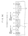
- Figs. 9A to 9D are schematic partial cross-sectional views of a semiconductor substrate for explaining the manufacturing steps of the semiconductor device of the eighth embodiment of the present invention.
- The present invention will then be explained on the basis of the preferred embodiments with reference to the accompanying drawings. Embodiment one relates to a semiconductor photosensitive element and a method for forming the same depending on the first profile of the present invention. Embodiment two relates to a semiconductor photosensitive element and a method for forming the same depending on the second profile of the present invention. Embodiment three relates to a semiconductor device including a semiconductor photosensitive element and a method for forming the same depending on the first profile of the present invention. Embodiment four relates to a semiconductor device including a semiconductor photosensitive element and a method for forming the same depending on the second profile of the present invention. In the embodiments described hereunder, the p type conductivity is selected as the first conductivity type and the n type conductivity as the second conductivity type.
- The semiconductor photosensitive element of the present invention has a first and a second photosensitive regions. The first photosensitive region has a structure different from the second photosensitive region and thereby has the photoelectric conversion characteristic and the frequency characteristic different from those of the second photosensitive region. In more practical terms, the first photosensitive region has the excellent frequency characteristic in comparison with the second photosensitive region. Meanwhile, the second photosensitive region has the excellent photoelectric conversion characteristic in comparison with the first photosensitive region.
- Embodiment one relates to a semiconductor photosensitive element and a method for forming the same depending on the first profile of the present invention. A schematic partial cross-sectional view of a semiconductor photosensitive element of embodiment one is shown in Fig. 2. The first photosensitive region is composed of a high
concentration impurity region 10 of a first conductivity type (p+ type) formed on a semiconductor substrate 1 of the first conductivity type (p type) and a photoelectric conversion layer 11 of a second conductivity type (n type) formed on the highconcentration impurity region 10. Meanwhile, the second photosensitive region is formed of aphotoelectric conversion layer 21 of the second conductivity type (n type) which is formed, on the semiconductor substrate 1, thicker than the photoelectric conversion layer 11 forming the first photosensitive region. The photosensitive regions are isolated by anelement isolation region 30 formed therebetween. In Fig. 2, a couple of the first photosensitive regions and a couple of the second photosensitive regions are illustrated. - The thickness of the photoelectric conversion layer 11 forming the first photosensitive region is set, for example, to 2 µm, while the thickness of the
photoelectric conversion layer 21 forming the second photosensitive region is set, for example, to 4 µm. Moreover, an impurity concentration of the semiconductor substrate 1 is set to 3 x 10¹⁵/cm3, while an impurity concentration of the highconcentration impurity region 10 to 5 x 10¹⁸/cm3 and an impurity concentration of the photoelectric conversion layers 11 and 21 to 5 x 10¹⁵/cm3. It has thereby been confirmed that the first photosensitive region operates with the frequency up to 30 MHz. However, the photoelectric conversion characteristic of the first photosensitive region has been 0.2A/W. Meanwhile, the photoelectric conversion characteristic of the second photosensitive region was 0.4A/W. However, it has also been confirmed that the first photosensitive region operates only with the frequency under 3 MHz. - In regard to the six photosensitive regions A, B, C, D, E, and F of the semiconductor photosensitive element for compact disc apparatus shown in Fig. 1A, four photosensitive regions A, B, C, and D correspond to the first photosensitive region. Meanwhile, the photosensitive regions E and F correspond to the second photosensitive region. In regard to eight photosensitive regions A, B, C, D, E, F, G, and H of the semiconductor photosensitive element for minidisc apparatus, the photosensitive regions G and H correspond to the first photosensitive region, while the photosensitive regions E and F correspond to the second photosensitive region. The photosensitive regions A, B, C and D are irradiated with an intensive light beam and the focus error signal has a comparatively lower frequency. Therefore, higher photoelectric conversion and frequency characteristics are not required for such photosensitive regions. Accordingly, the photosensitive regions A, B, C, and D may have the structure of the first photosensitive region or the second photosensitive region.
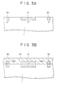
- Embodiment two of the present invention disclosing a method for forming a semiconductor photosensitive element as embodiment one will be explained with reference to a schematic partial cross-sectional view of a semiconductor substrate shown in Figs. 3A and 3B.
- First, a high
concentration impurity region 10 of the first conductivity type (p+ type) and anelement isolation region 30 are to be formed on a silicon semiconductor substrate 1 of the first conductivity type (p type) (Fig. 3A). For this purpose, a mask, provided with an aperture (not illustrated) in the region where the highconcentration impurity region 10 andelement isolation region 30 are to be formed, is formed on the surface of the semiconductor substrate 1. Thereafter, a high concentration p type impurity (for example, boron) is diffused or ion implanted to the semiconductor substrate 1 to form the highconcentration impurity region 10 of the first conductivity type (p+ type) and theelement isolation region 30. This highconcentration impurity region 10 is a buried type. - Thereafter, a
semiconductor layer 40 of the second conductivity type (n type) is formed (Fig. 3B), for example, by the CVD method on the semiconductor substrate 1 including theelement isolation region 30 and the highconcentration impurity region 10. Thesemiconductor layer 40 is composed of an n-type single crystal silicon epitaxially grown by the CVD method. In the CVD method, the SiH4/H2 gas is used, for example, as the raw gas, while AsH3 gas as the doping gas. Thesemiconductor layer 40 is formed on the semiconductor substrate 1 in the thickness of 4 µm. While thesemiconductor layer 40 is epitaxially grown, a part of thesemiconductor layer 40 above the highconcentration impurity region 10 and theelement isolation region 30 comes to have the first conductivity type (p+ type) due to outer diffusion and auto-doping of the p type impurity. As a result, thesemiconductor layer 40 of the second conductivity type (n type) above the highconcentration impurity region 10 and theclement isolation region 30 is reduced in thickness to about 2µm. - Thereafter, in order to complete the
clement isolation region 30, a mask (not illustrated) is provided on thesemiconductor layer 40 above theelement isolation region 30 and then boron is ion-implanted thereto. As explained above, a first photosensitive region formed of the photoelectric conversion region 11 composed of the highconcentration impurity region 10 formed on the semiconductor substrate 1 and thesemiconductor layer 40 formed on theimpurity region 10 and a second photosensitive region formed of thephotoelectric conversion layer 21 composed of thesemiconductor layer 40 formed on the semiconductor substrate 1 are formed (Fig. 2). Thereafter, an anode terminal and a cathode terminal (not illustrated) are formed with aluminum or aluminum alloy to each photosensitive region by the known method and the surface of each photosensitive region is covered with a covering material (not illustrated) for the protection purpose. - Embodiment three relates to a semiconductor photosensitive element depending on the second profile of the present invention and a method for forming the same. A schematic partial cross-sectional view of a semiconductor photosensitive element of embodiment three is shown in Fig. 4. The first photosensitive region is composed of a high
concentration impurity region 12 of the second conductivity type (n+ type) formed on a semiconductor substrate 1 of the first conductivity type (p type), aphotoelectric conversion layer 13 of the second conductivity type (n type) formed on the highconcentration impurity region 12 and a first conductivity type layer (p+ type layer) 14 formed thephotoelectric conversion layer 13. Meanwhile, the second photosensitive region is formed of aphotoelectric conversion layer 21 of the second conductivity type (n type) formed, on the semiconductor substrate 1, thicker than thephotoelectric conversion layer 13 forming the first photosensitive region. Moreover, the photosensitive regions are isolated by anelement isolation region 30. Fig. 4 illustrates a couple of the first photosensitive regions and a couple of the second photosensitive regions. - The
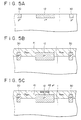
photoelectric conversion layer 13 forming the first photosensitive region is formed, for example, in the thickness of 2 µm, while thephotoelectric conversion layer 21 forming the second photosensitive region is formed, for example, in the thickness of 4 µm. Moreover, the semiconductor substrate 1 is given the impurity concentration of 3 x 10¹⁵/cm3, while the highconcentration impurity region 10 is given the impurity concentration of 5 x 10¹⁸/cm3 and the photoelectric conversion layers 13 and 14 are given the impurity concentration of 7 x 10¹⁷/cm3, respectively. - Embodiment four of the present invention disclosing a method for forming a semiconductor photosensitive element as embodiment three will be explained with reference to a schematic partial cross-sectional view of the semiconductor substrate shown in Figs. 5A to 5C.
- First, a high
concentration impurity region 12 of the second conductivity type (n+ type) and anelement isolation region 30 of the first conductivity type (p+ type) are to be formed on a silicon semiconductor substrate 1 of the first conductivity type (p type) (Fig. 5A). For this purpose, a mask provided with an aperture in the region where the highconcentration impurity region 12 is to be formed (not illustrated) is formed on the surface of the semiconductor substrate 1. Thereafter, a high concentration n type impurity (for example, arsenic) is diffused or ion-implanted to the semiconductor substrate 1 to form the highconcentration impurity region 12 of the second conductivity type (n+ type). Next, a mask provided with an aperture in the region where theelement isolation region 30 is to be formed (not illustrated) is formed on the surface of the semiconductor substrate 1. Thereafter, a high concentration p type impurity (for example, boron) is diffused or ion-implanted to the semiconductor substrate 1 to form anelement isolation region 30 of the first conductivity type (p+ type). Here, the formation sequence of the highconcentration impurity region 12 andclement isolation region 30 may be inverted. This highconcentration impurity region 12 is of the buried type. - Subsequently, a
first semiconductor layer 41 of the second conductivity type (n type) is formed, for example, by the CVD method on the semiconductor substrate 1 including theelement isolation region 30 and the high concentration impurity region 12 (Fig. 5B). Thefirst semiconductor layer 41 is formed of an n type single crystal silicon epitaxially grown by the CVD method. In the CVD method, SiH4/H2 gas, for example, is used as the raw gas, while the AsH3 gas as the doping gas. Thefirst semiconductor layer 41 is formed on the semiconductor substrate 1 in the thickness of 4 µm. While thefirst semiconductor layer 41 is epitaxially grown, a part of thefirst semiconductor layer 41 above the highconcentration impurity region 12 andelement isolation region 30 comes to have the second conductivity type (n+ type) and the first conductivity type (p+ type) due to the outer diffusion and auto-doping of the p type impurity. As a result, thefirst semiconductor layer 41 of the second conductivity type (n type) above the highconcentration impurity region 12 andelement isolation region 30 is reduced in the thickness to about 2 µm. - Next, a
second semiconductor layer 42 of the first conductivity type (p+ type) is formed on thefirst semiconductor layer 41 above the high concentration impurity region 12 (Fig. 5C). Thesecond semiconductor layer 42 may be formed by diffusion or ion-implantation of the p type impurity (for example, boron) into thefirst semiconductor layer 41. - Thereafter, in order to complete the
element isolation region 30, a mask (not illustrated) is provided on thefirst semiconductor layer 41 above theclement isolation region 30 and boron is ion-implanted to the mask. Thereby, the first photosensitive region is formed of the highconcentration impurity region 12 formed on the semiconductor substrate 1, thephotoelectric conversion layer 13 composed offirst semiconductor layer 41 formed on the impurity region and the second semiconductor layer 42 (first conductivity type layer 14) formed on thephotoelectric conversion layer 13. In addition, the second photosensitive region formed of thephotoelectric conversion layer 21 composed of thefirst semiconductor layer 41 formed on the semiconductor substrate 1 is also formed (Fig. 3). An anode terminal and a cathode terminal (not illustrated) are formed to each photosensitive region with aluminum or aluminum alloy by the known method to cover the surface of each photosensitive region with a covering material (not illustrated) for the protection purpose. Here, the ion-implantation for completing theelement isolation region 30 may be executed before the [Step 220]. - Embodiment five relates to a semiconductor device depending on the first profile of the present invention and a method for forming the same. The schematic partial cross-sectional view of the semiconductor device of embodiment five is shown in Fig. 6. The structures of the first and second photosensitive regions are the same as the structure of each photosensitive region explained with respect to embodiment one and detail explanation about the structures is omitted here. The semiconductor device of embodiment five is defined as a bipolar transistor, in more practical terms, a vertical npn type bipolar transistor formed on the high
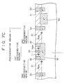
concentration impurity region 50 of the second conductivity type (n+ type) formed on the semiconductor substrate 1 of the first conductivity type (p type). - A method for forming the semiconductor device of embodiment five is substantially the same as a method for forming the semiconductor photosensitive element explained as embodiment one, except for the point that the manufacturing step of the semiconductor element is included. A method for forming the semiconductor device of embodiment five will be explained with reference to Figs. 7A to 7C.
- First, a high
concentration impurity region 10 of the first conductivity type (n+ type) and anelement isolation region 30 are to be formed on a silicon semiconductor substrate 1 of the first conductivity type (p type). For this purpose, a mask provided with an aperture in the region where the highconcentration impurity region 10 andelement isolation region 30 are to be formed (not illustrated) is formed on the surface of the semiconductor substrate 1. A high concentration p type impurity (for example, boron) is diffused or ion-implanted to the semiconductor substrate 1 to form the highconcentration impurity region 12 of the first conductivity type (p+ type) and theelement isolation region 30. Next, a mask provided with an aperture in the region where a second highconcentration impurity region 50 is to be formed (not illustrated) is formed on the surface of the semiconductor substrate 1. A high concentration n type impurity (for example, arsenic) is then diffused or ion-implanted to the semiconductor substrate 1 to form the second highconcentration impurity region 50 of the second conductivity type (n+ type) (Fig. 7A). Formation of the first highconcentration impurity region 10 of the first conductivity type andelement isolation region 30 and formation of the second highconcentration impurity region 50 of the second conductivity type may be executed in the inverted sequence. These highconcentration impurity regions concentration impurity region 50 provides a low resistance path extending to the collector from an active region of a bipolar transistor as the semiconductor clement to be formed later. - Next, a
semiconductor layer 40 of the second conductivity type (n type) is formed on the semiconductor substrate 1 including theelement isolation region 30 and the first and second highconcentration impurity regions 10 and 50 (Fig. 7B). This step may be executed in the same manner as the [Step 110] of embodiment one. - Thereafter, in order to complete the
element isolation layer 30, a mask (not illustrated) is provided on thesemiconductor layer 40 above theelement isolation region 30 and boron is ion-implanted to the mask. Thereby, the first photosensitive region, formed of the photoelectric conversion layer 11 composed of the first highconcentration impurity region 10 formed on the semiconductor substrate 1 and thesemiconductor layer 40 formed on the first highconcentration impurity region 10, may be formed. In addition, the second photosensitive region formed of thephotoelectric conversion layer 21 consisting of thesemiconductor layer 40 formed on the semiconductor substrate 1 may also be formed (fig. 7C). - Next, with the method of the related arts, a semiconductor element consisting of a vertical type npn bipolar transistor is to be formed on the
semiconductor layer 40 on the second highconcentration impurity region 50. For this purpose, abase 52 consisting of the p type conductive region is formed by diffusion or ion-implantation of the p type impurity (for example, boron) into thesemiconductor layer 40. Formation of the base 52 may be done simultaneously by ion-implantation of boron to complete theelement isolation region 30 in the [Step 320] (Fig. 7C). Next, acollector 51 and anemitter 53 consisting of the n+ type conductive region are formed by diffusion or ion-implantation of the n type impurity (for example, arsenic) into thesemiconductor layer 40 and a part of thebase 52. As explained above, the semiconductor device shown in Fig. 6 can be manufactured. - Thereafter, an anode terminal and a cathode terminal (not illustrated) are formed with aluminum or aluminum alloy by the known method to each photosensitive region and the surface of each photosensitive region is covered with a covering material (not illustrated) for the protection purpose. Meanwhile, electrodes are formed to the
collector 51,base 52 andemitter 53 of the semiconductor element and the semiconductor element and each photosensitive region are electrically connected, as required, with a wiring composed of a metal wiring material. - A schematic partial cross-sectional view of the semiconductor device of embodiment seven is illustrated in Fig. 8. The structures of the first and second photosensitive regions are similar to the structure of each photosensitive region explained regarding embodiment three and detail explanation thereof is omitted here. The semiconductor clement 6 of embodiment seven is also defined as a bipolar transistor, in more practical, a vertical npn type bipolar transistor formed above the high
concentration impurity region 50 of the second conductivity type (n+ type) formed on the semiconductor substrate 1 of the first conductivity type (p type). - A method for forming the semiconductor device of embodiment seven may substantially be set similar to the method for forming the semiconductor photosensitive element explained with reference to embodiment three, except for the point that the method for forming the semiconductor device is included. The method for forming the semiconductor device of embodiment seven will then be explained with reference to Figs. 9A to 9D.
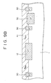
- First, a first high
concentration impurity region 12 and a second highconcentration impurity region 50 of the second conductivity type (n+ type) and anelement isolation region 30 of the first conductivity type (p+ type) are to be formed on a silicon semiconductor substrate 1 of the first conductivity type (p type) (Fig. 9A). For this purpose, a mask (not illustrated) provided with an aperture in the region where the first and second highconcentration impurity regions concentration impurity regions element isolation region 30 is to be formed is formed on the surface of the semiconductor substrate 1. Thereafter, theelement isolation region 30 of the first conductivity type (p+ type) is formed by diffusion or ion-implantation of the high concentration p type impurity (for example, boron) into the semiconductor substrate 1. Here, formation of the first and second highconcentration impurity regions element isolation region 30 may be inverted in the formation sequence. These highconcentration impurity regions - Next, a
first semiconductor layer 41 of the second conductivity type (n type) is formed on the semiconductor substrate 1 including theelement isolation region 30 and first and second highconcentration impurity regions 10 and 50 (Fig. 9B). This step may be similar to the [Step 210] of embodiment two. - Thereafter, in order to complete the
element isolation region 30, a mask (not illustrated) is provided on thefirst semiconductor layer 41 above theelement isolation region 30 and boron is then ion-implanted thereto. Thereby, the second photosensitive region formed of thephotoelectric conversion layer 21 consisting of thefirst semiconductor layer 41 formed on the semiconductor substrate 1 is formed (Fig. 9C). - Next, with the method of the related arts, a semiconductor element consisting of the vertical npn bipolar transistor is to be formed on the
first semiconductor layer 41 above the second highconcentration impurity region 50. For this purpose, abase 52 consisting of the p type conductive region is formed by diffusion or ion-implantation of the p type impurity (for example, boron) into thefirst semiconductor layer 41. Moreover, asecond semiconductor layer 42 of the first conductivity type (p+ type) is formed on thefirst semiconductor layer 41 above the first high concentration impurity region 12 (Fig. 9D). Thesecond semiconductor layer 42 may be formed simultaneously with the base 52 by diffusion or ion-implantation of the p type impurity (for example, boron) into thefirst semiconductor layer 41. Here, formation of thesecond semiconductor layer 42 may also be performed before or after the [Step 420], instead of simultaneous formation with thebase 52. Thereby, the first photosensitive region, formed of the first highconcentration impurity region 12 formed on the semiconductor substrate 1, thephotoelectric conversion layer 13 consisting of thefirst semiconductor layer 41 formed on the first highconcentration impurity region 12 and the second semiconductor layer 42 (first conductivity type layer 14) formed on thephotoelectric conversion layer 13, may be formed. - Next, the
collector 51 andemitter 53 consisting of the n+ type conductive region are formed by diffusion or ion-implantation of the n type impurity (for example, boron) into thefirst semiconductor layer 41 and a part of thebase 52. The semiconductor device illustrated in Fig. 8 may be formed as explained above. - Thereafter, an anode terminal and a cathode terminal (not illustrated) are formed to each photosensitive region with aluminum or aluminum alloy by the known method and the surface of each photosensitive region is covered with a covering material (not illustrated) for the protection purpose. On the other hand, electrodes are formed to the
collector 51,base 52 andemitter 53 of the semiconductor element and the semiconductor clement is electrically connected as required to each photosensitive region with a wiring 1 consisting of an metal wiring material. - The present invention has been explained on the basis of the preferred embodiments thereof. However, the present invention is not limited thereto and allows, as required, various modifications of numerical values explained in each embodiment and practical method disclosed in each step which are indicated only as the examples. In the embodiments explained above, the first conductivity type is defined as p type, while the second conductivity type as n type, but it is naturally possible to define the first conductivity type as n type, while the second conductivity type as p type. In the embodiments, moreover, a semiconductor element in the semiconductor device has been explained only as an example of the vertical npn type bipolar transistor, but the semiconductor clement is not limited thereto and may be explained as a variety of bipolar transistor such as a lateral pnp type bipolar transistor or as a field effect transistor.
- The semiconductor photosensitive element or semiconductor device of the present invention can be provided with a first photosensitive region having excellent frequency characteristic and a second photosensitive region having excellent photoelectric conversion characteristic. Thereby, the operation characteristic of the semiconductor photosensitive element or semiconductor device can be optimized, enabling improvement in total characteristic of the semiconductor photosensitive element or semiconductor device.
- In the method for forming the semiconductor device of the present invention, the manufacturing process, for example, of the bipolar transistor of the related art, the formation process of the
element isolation region 30 and the formation process of the semiconductor layer 40 (or first semiconductor layer 41) and thesecond semiconductor layer 42 may be introduced as the common process. Therefore, the first photosensitive region having excellent frequency characteristic and the second photosensitive region having excellent photoelectric conversion characteristic can be formed together with the semiconductor element only by modifying a little the conventional manufacturing process of the bipolar transistor. - Moreover, polarity of the signal outputted from the first photosensitive region can be changed by forming the first photosensitive region as the anode terminal common type or as the cathode terminal common type. Thereby, the amplifier for amplifying the signals outputted from the first photosensitive region and the signal processing circuit can be selected from wider range or the inverter for inverting polarity of signals can be ruled out.
Claims (17)
- A semiconductor photosensitive element comprising a first and a second photosensitive region (resp. (10, 11) and (21)), whereby said first photosensitive region is different from said second photosensitive region in structure and thereby said first photosensitive region has a photoelectric conversion characteristic and frequency characteristic which are different from those of said second photosensitive region, whereinsaid first photosensitive region is composed of a high concentration impurity region (10, 12) formed on a semiconductor substrate (1) of a first conductivity type and a first photoelectric conversion layer (11) of a second conductivity type formed on said impurity region;said second photosensitive region is composed of a second photoelectric conversion layer (21) of the second conductivity type, formed on said semiconductor substrate (1), thicker than the photoelectric conversion region consisting of said first photosensitive region; andrespective photosensitive regions are isolated by element isolation regions (30) formed therebetween.
- A semiconductor photosensitive element as recited in claim 1, further comprising a first conductivity type layer (14) formed on the first photoelectric conversion layer (11);
- A semiconductor device composed of a semiconductor photosensitive element as recited in claims 1 or 2 and a semiconductor element.
- A semiconductor device as recited in claim 3, comprising a signal processing circuit formed together with said semiconductor photosensitive element on the same substrate.
- An optical pickup device, comprising a semiconductor device as recited in claim 3.
- An optical recording and reproducing device, comprising an optical pickup device as recited in claim 5.
- A semiconductor device as recited in claim 3, comprising a bipolar transistor (51, 52, 53) formed above a high concentration impurity region (41) of the second conductivity type formed on said semiconductor substrate (1) of the first conductivity type.
- A semiconductor device as recited in claim 7, comprising a signal processing circuit utilizing a bipolar transistor (51, 52, 53) as said semiconductor element.
- A semiconductor device as recited in claim 3, comprising a photodiode for detecting focus error, tracking error or optical signal detection utilizing said semiconductor photosensitive element.
- A semiconductor device as recited in claim 8, comprising a current-voltage conversion circuit within said signal processing circuit utilizing said semiconductor element.
- An optical pickup device on which is mounted a semiconductor device as recited in claim 8.
- An optical recording and reproducing device, comprising an optical pickup device and a semiconductor device as recited in claim 8.
- A method for forming a semiconductor photosensitive element comprising the steps of:(A) forming a high concentration impurity region (10, 12) and an element isolation region (30) on a semiconductor substrate (1) of a first conductivity type;(B) forming a first semiconductor layer (40, 41) of the second conductivity type on said semiconductor substrate and high concentration impurity region, thereby to form; (a) a first photosensitive region formed of said high concentration impurity region (10, 12) formed on said semiconductor substrate (1) and a first photoelectric conversion layer (11, 13) consisting of said semiconductor layer formed on said impurity region; and (b) a second photosensitive region formed of a second photoelectric conversion layer (21) consisting of said semiconductor layer formed on said semiconductor substrate.
- A method for forming a semiconductor photosensitive element as recited in claim 13, further comprising the steps of:forming a second semiconductor layer (14) of the first conductivity type into the first semiconductor layer on said high concentration impurity region, thereby to form a second semiconductor layer formed on said photoelectric conversion layer.
- A method for forming a semiconductor device comprising steps of :(A) forming, on a semiconductor substrate (1) of the first conductivity type, a first high concentration impurity region (10, 12), an element isolation layer (30) and a second high concentration impurity region (50);(B) forming a first semiconductor layer (40, 41) of the second conductivity type on said semiconductor substrate and said first and second high concentration impurity regions, thereby to form; (a) a first photosensitive region formed of said first high concentration impurity region (10, 12) formed on said semiconductor substrate (1) and a first photoelectric conversion layer (11, 13) consisting of said semiconductor layer formed on said impurity region; and (b) a second photosensitive region formed of a second photoelectric conversion layer (21) consisting of said semiconductor layer formed on said semiconductor substrate; and(C) forming a semiconductor element on the first semiconductor layer (40, 41) above said second high concentration impurity region (50).
- A method for forming a semiconductor device as recited in claim 15 further comprising the steps of forming a second semiconductor layer (14) of the first conductivity type into the first semiconductor layer on the first high concentration impurity region to form a first photosensitive region formed of the photoelectric conversion layer (13) consisting of the first high concentration impurity region formed on said semiconductor substrate and the first semiconductor layer formed on said impurity region and a second semiconductor layer formed of said photoelectric conversion layer.
- A method for forming a semiconductor device as recited in claim 16 or 17, wherein said semiconductor element is a bipolar transistor.
Applications Claiming Priority (3)
| Application Number | Priority Date | Filing Date | Title |
|---|---|---|---|
| JP17183894 | 1994-06-30 | ||
| JP171838/94 | 1994-06-30 | ||
| JP6171838A JPH0818093A (en) | 1994-06-30 | 1994-06-30 | Semiconductor photoreceiver and semiconductor device and manufacture thereof |
Publications (3)
| Publication Number | Publication Date |
|---|---|
| EP0694974A2 EP0694974A2 (en) | 1996-01-31 |
| EP0694974A3 EP0694974A3 (en) | 1996-05-15 |
| EP0694974B1 true EP0694974B1 (en) | 2001-12-19 |
Family
ID=15930700
Family Applications (1)
| Application Number | Title | Priority Date | Filing Date |
|---|---|---|---|
| EP95401491A Expired - Lifetime EP0694974B1 (en) | 1994-06-30 | 1995-06-23 | Photosensor and method for forming the same |
Country Status (7)
| Country | Link |
|---|---|
| US (4) | US5898209A (en) |
| EP (1) | EP0694974B1 (en) |
| JP (1) | JPH0818093A (en) |
| KR (1) | KR100385306B1 (en) |
| DE (1) | DE69524684T2 (en) |
| MY (1) | MY117089A (en) |
| SG (2) | SG63728A1 (en) |
Families Citing this family (23)
| Publication number | Priority date | Publication date | Assignee | Title |
|---|---|---|---|---|
| JP2882354B2 (en) * | 1996-04-30 | 1999-04-12 | 日本電気株式会社 | Integrated circuit device with built-in light receiving element |
| JP3170463B2 (en) * | 1996-09-30 | 2001-05-28 | シャープ株式会社 | Photodetector with built-in circuit |
| JP3918220B2 (en) * | 1997-02-27 | 2007-05-23 | ソニー株式会社 | Semiconductor device and manufacturing method thereof |
| US5994162A (en) * | 1998-02-05 | 1999-11-30 | International Business Machines Corporation | Integrated circuit-compatible photo detector device and fabrication process |
| US6034407A (en) * | 1998-07-31 | 2000-03-07 | Boeing North American, Inc. | Multi-spectral planar photodiode infrared radiation detector pixels |
| EP0986110A1 (en) * | 1998-09-10 | 2000-03-15 | Electrowatt Technology Innovation AG | Light receiving semiconductor device and its use in flame control |
| US6118142A (en) * | 1998-11-09 | 2000-09-12 | United Microelectronics Corp. | CMOS sensor |
| US6168966B1 (en) * | 1999-02-18 | 2001-01-02 | Taiwan Semiconductor Manufacturing Company | Fabrication of uniform areal sensitivity image array |
| JP3317942B2 (en) * | 1999-11-08 | 2002-08-26 | シャープ株式会社 | Semiconductor device and manufacturing method thereof |
| JP4208172B2 (en) * | 2000-10-31 | 2009-01-14 | シャープ株式会社 | Photodiode and light receiving element with built-in circuit using the same |
| US7212240B1 (en) | 2001-05-25 | 2007-05-01 | Dalsa, Inc. | Imager with a row of photodiodes or pinned photo diodes |
| US6504196B1 (en) * | 2001-08-30 | 2003-01-07 | Micron Technology, Inc. | CMOS imager and method of formation |
| US6960796B2 (en) * | 2002-11-26 | 2005-11-01 | Micron Technology, Inc. | CMOS imager pixel designs with storage capacitor |
| KR100685892B1 (en) * | 2005-06-07 | 2007-02-26 | 동부일렉트로닉스 주식회사 | CMOS image sensor and method for manufacturing the same |
| JP4618064B2 (en) * | 2005-09-12 | 2011-01-26 | ソニー株式会社 | Semiconductor device and manufacturing method thereof |
| US7652313B2 (en) * | 2005-11-10 | 2010-01-26 | International Business Machines Corporation | Deep trench contact and isolation of buried photodetectors |
| JP4396684B2 (en) * | 2006-10-04 | 2010-01-13 | ソニー株式会社 | Method for manufacturing solid-state imaging device |
| JP5566457B2 (en) * | 2010-06-18 | 2014-08-06 | 富士フイルム株式会社 | Solid-state imaging device and digital camera |
| FR2969821A1 (en) * | 2010-12-23 | 2012-06-29 | St Microelectronics Sa | PHOTOCITY MATRIX IMAGING DEVICE WITH CHARGING TRANSFER MONOCOUP CONTROLS |
| JP6119184B2 (en) * | 2012-10-19 | 2017-04-26 | 株式会社ニコン | Solid-state imaging device, imaging apparatus, and manufacturing method of solid-state imaging device |
| EP3651213A4 (en) * | 2017-08-09 | 2020-05-20 | Kaneka Corporation | Photoelectric conversion element and photoelectric conversion device |
| WO2019053959A1 (en) * | 2017-09-13 | 2019-03-21 | 株式会社カネカ | Photoelectric conversion element and photoelectric conversion device |
| CN111052403B (en) | 2017-11-15 | 2023-01-31 | 株式会社钟化 | Photoelectric conversion device |
Family Cites Families (26)
| Publication number | Priority date | Publication date | Assignee | Title |
|---|---|---|---|---|
| US3448344A (en) * | 1966-03-15 | 1969-06-03 | Westinghouse Electric Corp | Mosaic of semiconductor elements interconnected in an xy matrix |
| JPS51113481A (en) * | 1975-03-28 | 1976-10-06 | Sony Corp | Semiconductor device |
| CA1119493A (en) * | 1978-07-21 | 1982-03-09 | Mamoru Fujieda | Fuel injection system for internal combustion engine |
| JPS5638697A (en) * | 1979-09-05 | 1981-04-13 | Mitsubishi Electric Corp | Detector for number of passed articles |
| DE3167682D1 (en) * | 1980-04-22 | 1985-01-24 | Semiconductor Res Found | Semiconductor image sensor |
| US4527182A (en) * | 1980-09-19 | 1985-07-02 | Nippon Electric Co., Ltd. | Semiconductor photoelectric converter making excessive charges flow vertically |
| EP0075192B1 (en) * | 1981-09-17 | 1990-03-14 | Kabushiki Kaisha Toshiba | An optical head |
| JPS5963778A (en) * | 1982-10-01 | 1984-04-11 | Hamamatsu Tv Kk | Silicon photodiode device and manufacture thereof |
| JPS59108344A (en) * | 1982-12-14 | 1984-06-22 | Olympus Optical Co Ltd | Solid-state image pickup element |
| US5210434A (en) * | 1983-07-02 | 1993-05-11 | Canon Kabushiki Kaisha | Photoelectric converter with scanning circuit |
| JPS6097681A (en) * | 1983-10-31 | 1985-05-31 | Matsushita Electric Works Ltd | Monolithic integrated circuit |
| JPS6161457A (en) * | 1984-09-01 | 1986-03-29 | Canon Inc | Photosensor and manufacture thereof |
| US5268309A (en) * | 1984-09-01 | 1993-12-07 | Canon Kabushiki Kaisha | Method for manufacturing a photosensor |
| JPH0654957B2 (en) * | 1985-11-13 | 1994-07-20 | キヤノン株式会社 | Photoelectric conversion device |
| DE3706278A1 (en) * | 1986-02-28 | 1987-09-03 | Canon Kk | Semiconductor device and method of fabricating it |
| JP2757985B2 (en) * | 1986-10-01 | 1998-05-25 | ソニー株式会社 | Light receiving device and manufacturing method thereof |
| JPS63122267A (en) * | 1986-11-12 | 1988-05-26 | Canon Inc | Optical sensor |
| JPS63132455U (en) * | 1987-02-20 | 1988-08-30 | ||
| JPS63299163A (en) * | 1987-05-28 | 1988-12-06 | Nec Corp | Photosemiconductor integrated circuit |
| JPH01211966A (en) * | 1988-02-18 | 1989-08-25 | Fujitsu Ltd | Solid-state sensing element and manufacture thereof |
| JPH01273364A (en) * | 1988-04-25 | 1989-11-01 | Clarion Co Ltd | Photodiode array and manufacture thereof |
| JPH02187079A (en) * | 1989-01-13 | 1990-07-23 | Sharp Corp | Photodiode |
| NL8901400A (en) * | 1989-06-02 | 1991-01-02 | Philips Nv | SEMICONDUCTOR DEVICE WITH A RADIATION-SENSITIVE ELEMENT. |
| US5410175A (en) * | 1989-08-31 | 1995-04-25 | Hamamatsu Photonics K.K. | Monolithic IC having pin photodiode and an electrically active element accommodated on the same semi-conductor substrate |
| JPH05145051A (en) * | 1991-11-18 | 1993-06-11 | Sanyo Electric Co Ltd | Optical semiconductor device |
| JPH05206500A (en) * | 1992-01-28 | 1993-08-13 | Nippondenso Co Ltd | Photoelectric conversion module |
-
1994
- 1994-06-30 JP JP6171838A patent/JPH0818093A/en active Pending
-
1995
- 1995-06-13 US US08/489,875 patent/US5898209A/en not_active Expired - Lifetime
- 1995-06-15 SG SG1997002581A patent/SG63728A1/en unknown
- 1995-06-15 SG SG1995000642A patent/SG52152A1/en unknown
- 1995-06-23 DE DE69524684T patent/DE69524684T2/en not_active Expired - Lifetime
- 1995-06-23 EP EP95401491A patent/EP0694974B1/en not_active Expired - Lifetime
- 1995-06-23 KR KR1019950017111A patent/KR100385306B1/en not_active IP Right Cessation
- 1995-06-28 MY MYPI95001785A patent/MY117089A/en unknown
-
1997
- 1997-05-27 US US08/863,354 patent/US6097074A/en not_active Expired - Lifetime
- 1997-05-27 US US08/863,310 patent/US5858810A/en not_active Expired - Lifetime
- 1997-05-27 US US08/863,587 patent/US5825071A/en not_active Expired - Lifetime
Also Published As
| Publication number | Publication date |
|---|---|
| US6097074A (en) | 2000-08-01 |
| KR960002909A (en) | 1996-01-26 |
| US5858810A (en) | 1999-01-12 |
| KR100385306B1 (en) | 2003-09-13 |
| SG63728A1 (en) | 1999-03-30 |
| SG52152A1 (en) | 1998-09-28 |
| EP0694974A3 (en) | 1996-05-15 |
| DE69524684D1 (en) | 2002-01-31 |
| JPH0818093A (en) | 1996-01-19 |
| MY117089A (en) | 2004-05-31 |
| DE69524684T2 (en) | 2002-08-08 |
| US5898209A (en) | 1999-04-27 |
| US5825071A (en) | 1998-10-20 |
| EP0694974A2 (en) | 1996-01-31 |
Similar Documents
| Publication | Publication Date | Title |
|---|---|---|
| EP0694974B1 (en) | Photosensor and method for forming the same | |
| US4831430A (en) | Optical semiconductor device and method of manufacturing the same | |
| US7982276B2 (en) | Optical semiconductor device and method for manufacturing the same | |
| US6380603B1 (en) | Photosensitive device with internal circuitry that includes on the same substrate | |
| US7928511B2 (en) | Semiconductor device and method for manufacturing semiconductor device | |
| US6376871B1 (en) | Semiconductor device having photodetector and optical pickup system using the same | |
| KR100428926B1 (en) | Circuit-incorporating light receiving device | |
| US4649409A (en) | Photoelectric transducer element | |
| US7851839B2 (en) | High-sensitivity image sensor and fabrication method thereof | |
| US4903103A (en) | Semiconductor photodiode device | |
| US20060151814A1 (en) | Optical semiconductor device | |
| JP3510500B2 (en) | Method for manufacturing semiconductor light receiving device | |
| JP2568074B2 (en) | Optical sensor integrated circuit | |
| JP2957834B2 (en) | Photodetector with built-in circuit | |
| JPH05145051A (en) | Optical semiconductor device | |
| JP4100474B2 (en) | Optical semiconductor device and manufacturing method thereof | |
| JP2839413B2 (en) | Photodetector with built-in circuit | |
| JPH04151874A (en) | Semiconductor device | |
| US5593902A (en) | Method of making photodiodes for low dark current operation having geometric enhancement | |
| JP3553715B2 (en) | Optical semiconductor device | |
| JP3086514B2 (en) | Optical semiconductor device | |
| JPH09321265A (en) | Semiconductor device | |
| JP2002280536A (en) | Optical semiconductor device | |
| JPH02254767A (en) | Optical semiconductor device | |
| KR20020048342A (en) | PIN Diode, PhotoDetector Using PIN Diode And Manufacturing Method Thereof |
Legal Events
| Date | Code | Title | Description |
|---|---|---|---|
| PUAI | Public reference made under article 153(3) epc to a published international application that has entered the european phase |
Free format text: ORIGINAL CODE: 0009012 |
|
| AK | Designated contracting states |
Kind code of ref document: A2 Designated state(s): DE FR GB |
|
| PUAL | Search report despatched |
Free format text: ORIGINAL CODE: 0009013 |
|
| AK | Designated contracting states |
Kind code of ref document: A3 Designated state(s): DE FR GB |
|
| 17P | Request for examination filed |
Effective date: 19961025 |
|
| 17Q | First examination report despatched |
Effective date: 19980409 |
|
| GRAG | Despatch of communication of intention to grant |
Free format text: ORIGINAL CODE: EPIDOS AGRA |
|
| GRAG | Despatch of communication of intention to grant |
Free format text: ORIGINAL CODE: EPIDOS AGRA |
|
| GRAH | Despatch of communication of intention to grant a patent |
Free format text: ORIGINAL CODE: EPIDOS IGRA |
|
| GRAH | Despatch of communication of intention to grant a patent |
Free format text: ORIGINAL CODE: EPIDOS IGRA |
|
| GRAA | (expected) grant |
Free format text: ORIGINAL CODE: 0009210 |
|
| AK | Designated contracting states |
Kind code of ref document: B1 Designated state(s): DE FR GB |
|
| REG | Reference to a national code |
Ref country code: GB Ref legal event code: IF02 |
|
| REF | Corresponds to: |
Ref document number: 69524684 Country of ref document: DE Date of ref document: 20020131 |
|
| ET | Fr: translation filed | ||
| PLBE | No opposition filed within time limit |
Free format text: ORIGINAL CODE: 0009261 |
|
| STAA | Information on the status of an ep patent application or granted ep patent |
Free format text: STATUS: NO OPPOSITION FILED WITHIN TIME LIMIT |
|
| 26N | No opposition filed | ||
| PGFP | Annual fee paid to national office [announced via postgrant information from national office to epo] |
Ref country code: FR Payment date: 20110630 Year of fee payment: 17 |
|
| PGFP | Annual fee paid to national office [announced via postgrant information from national office to epo] |
Ref country code: GB Payment date: 20110620 Year of fee payment: 17 |
|
| PGFP | Annual fee paid to national office [announced via postgrant information from national office to epo] |
Ref country code: DE Payment date: 20110622 Year of fee payment: 17 |
|
| GBPC | Gb: european patent ceased through non-payment of renewal fee |
Effective date: 20120623 |
|
| REG | Reference to a national code |
Ref country code: FR Ref legal event code: ST Effective date: 20130228 |
|
| REG | Reference to a national code |
Ref country code: DE Ref legal event code: R119 Ref document number: 69524684 Country of ref document: DE Effective date: 20130101 |
|
| PG25 | Lapsed in a contracting state [announced via postgrant information from national office to epo] |
Ref country code: FR Free format text: LAPSE BECAUSE OF NON-PAYMENT OF DUE FEES Effective date: 20120702 Ref country code: DE Free format text: LAPSE BECAUSE OF NON-PAYMENT OF DUE FEES Effective date: 20130101 Ref country code: GB Free format text: LAPSE BECAUSE OF NON-PAYMENT OF DUE FEES Effective date: 20120623 |