EP1079430B1 - A method of manufacturing a semiconductor device - Google Patents
A method of manufacturing a semiconductor device Download PDFInfo
- Publication number
- EP1079430B1 EP1079430B1 EP00302139A EP00302139A EP1079430B1 EP 1079430 B1 EP1079430 B1 EP 1079430B1 EP 00302139 A EP00302139 A EP 00302139A EP 00302139 A EP00302139 A EP 00302139A EP 1079430 B1 EP1079430 B1 EP 1079430B1
- Authority
- EP
- European Patent Office
- Prior art keywords
- areas
- area
- pads
- chip
- cut
- Prior art date
- Legal status (The legal status is an assumption and is not a legal conclusion. Google has not performed a legal analysis and makes no representation as to the accuracy of the status listed.)
- Expired - Lifetime
Links
Images








Classifications
-
- H—ELECTRICITY
- H10—SEMICONDUCTOR DEVICES; ELECTRIC SOLID-STATE DEVICES NOT OTHERWISE PROVIDED FOR
- H10P—GENERIC PROCESSES OR APPARATUS FOR THE MANUFACTURE OR TREATMENT OF DEVICES COVERED BY CLASS H10
- H10P74/00—Testing or measuring during manufacture or treatment of wafers, substrates or devices
- H10P74/27—Structural arrangements therefor
- H10P74/273—Interconnections for measuring or testing, e.g. probe pads
-
- H—ELECTRICITY
- H10—SEMICONDUCTOR DEVICES; ELECTRIC SOLID-STATE DEVICES NOT OTHERWISE PROVIDED FOR
- H10B—ELECTRONIC MEMORY DEVICES
- H10B20/00—Read-only memory [ROM] devices
-
- H—ELECTRICITY
- H10—SEMICONDUCTOR DEVICES; ELECTRIC SOLID-STATE DEVICES NOT OTHERWISE PROVIDED FOR
- H10W—GENERIC PACKAGES, INTERCONNECTIONS, CONNECTORS OR OTHER CONSTRUCTIONAL DETAILS OF DEVICES COVERED BY CLASS H10
- H10W72/00—Interconnections or connectors in packages
- H10W72/90—Bond pads, in general
-
- H—ELECTRICITY
- H10—SEMICONDUCTOR DEVICES; ELECTRIC SOLID-STATE DEVICES NOT OTHERWISE PROVIDED FOR
- H10W—GENERIC PACKAGES, INTERCONNECTIONS, CONNECTORS OR OTHER CONSTRUCTIONAL DETAILS OF DEVICES COVERED BY CLASS H10
- H10W72/00—Interconnections or connectors in packages
- H10W72/071—Connecting or disconnecting
- H10W72/075—Connecting or disconnecting of bond wires
- H10W72/07551—Connecting or disconnecting of bond wires characterised by changes in properties of the bond wires during the connecting
- H10W72/07554—Connecting or disconnecting of bond wires characterised by changes in properties of the bond wires during the connecting changes in dispositions
-
- H—ELECTRICITY
- H10—SEMICONDUCTOR DEVICES; ELECTRIC SOLID-STATE DEVICES NOT OTHERWISE PROVIDED FOR
- H10W—GENERIC PACKAGES, INTERCONNECTIONS, CONNECTORS OR OTHER CONSTRUCTIONAL DETAILS OF DEVICES COVERED BY CLASS H10
- H10W72/00—Interconnections or connectors in packages
- H10W72/50—Bond wires
- H10W72/541—Dispositions of bond wires
- H10W72/547—Dispositions of multiple bond wires
-
- H—ELECTRICITY
- H10—SEMICONDUCTOR DEVICES; ELECTRIC SOLID-STATE DEVICES NOT OTHERWISE PROVIDED FOR
- H10W—GENERIC PACKAGES, INTERCONNECTIONS, CONNECTORS OR OTHER CONSTRUCTIONAL DETAILS OF DEVICES COVERED BY CLASS H10
- H10W72/00—Interconnections or connectors in packages
- H10W72/90—Bond pads, in general
- H10W72/931—Shapes of bond pads
- H10W72/932—Plan-view shape, i.e. in top view
Definitions
- the present invention relates to a method of manufacturing a semiconductor device. More particularly this invention relates to a method of manufacturing a semiconductor device such as IC (integrated circuit) chips used for IC cards.
- IC integrated circuit
- IC cards such as, for example, railway ticket cards and electronic money cards in the field of electronic commerce.
- the IC cards are mounted with IC chips that store various kinds of information.
- the IC chips are generally constructed of nonvolatile memories, such as, for example, ferroelectric memories (FeRAM).
- Information about fare and a section of a railway a person travels, etc. are stored in the IC chips used as the railway ticket card.
- Information about a password, amount, a bank account number, a credit number, etc. is stored in IC chips used as the electronic money card. It is important that this information must not be made known to other persons, and that the information regarding money can not be rewritten by a third party.
- a plurality of square chip areas each chip area having a size of the order of a few millimeters on one side, are formed on a semiconductor wafer.
- the IC chips are then manufactured by cutting and separating these chip areas.
- Fig. 1 is a top plan view schematically illustrating an enlarged main portion of a prior-art semiconductor wafer.
- a plurality of chip areas 11 are formed on a semiconductor wafer 1.
- circuit elements such as transistors are formed in each chip area 11.
- a plurality of pads 12 are also formed within each chip area 11.
- the pads 12 are electrically connected to various circuit elements with wires 13.
- Four pads 12 are illustrated in this figure. However, in general, several to a hundred pads 12 are present in one wafer.
- a scribe area 14 is formed between the chip areas 11.
- the wafer 1 is cut along the scribe areas 14 using a diamond cutter or using laser beams at the time of dicing. Individual IC chips are obtained by such cutting.
- EP-A-0438 127 describes a semiconductor wafer, wherein upon the making of a die-sort testing for a predetermined IC pattern formed on each chip area; a plurality of sets of output pads selectively supplied with output signals are formed on the chip area and connected with a connection pattern on a dicing line area, and one testing pad is provided for the respective set of the pads.
- the IC patterns are tested by electrically contacting the testing pad with corresponding probe needle of probe card in a die-sort machine.
- WO 83/00244 describes an integrated circuit chip having a digital memory wherein direct access to at least a portion of the memory is prevented.
- Contact pads having coupling lines to couple the contact pads to the memory bus are provided.
- a security code can be programmed into a portion of the memory during wafer probe and test. When the integrated circuit chip is removed from the wafer the coupling lines between the contact pads and the memory bus are destroyed since the coupling lines are made to extend off of the chip.
- Embodiments of the present invention aim to provide a method of manufacturing a semiconductor device capable of preventing highly secret information written in the semiconductor device before dicing from being read out or corrupted after dicing.
- the pads and the lead wires may be formed on the same metal wired layer. Alternatively, the pads and the lead wires may be formed on different wired layers, and they are electrically connected together through contact sections. Alternatively the lead wires may be formed on a plurality of divided wired layers, and the lead wires are electrically connected with the pads through contact sections.
- the invention even if a part of the pad remains in the semiconductor chip after dicing, it is possible to isolate this pad from the inside memory area. Accordingly, after the semiconductor wafer has been disconnected to obtain the semiconductor chips, it is possible to prevent more securely the written data from being read out from the memory areas of the semiconductor chips and to prevent corruption of the written data.
- a part of the lead wires is disconnected together with the scribe area at the time of dicing, so that the lead wires are separated from the pads.
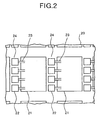
- Fig. 2 is a top plan view schematically illustrating an enlarged main portion of a semiconductor wafer manufactured using the method of a first example which is not an embodiment of the present invention.
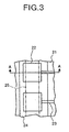
- Fig. 3 is a top plan view schematically illustrating an enlarged part of a scribe area of the semiconductor wafer shown in Fig. 2 .
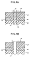
- Fig. 4A and Fig. 4B are vertical cross-sectional views of a portion cut along a line A-A of the semiconductor wafer shown in Fig.3 .
- Fig. 4A shows a state before dicing
- Fig. 4B shows a state after dicing.
- a plurality of chip areas 21 are formed on a semiconductor wafer 20.
- circuit elements such as transistors (not shown).
- a memory area is constructed of the circuit elements. This memory area is used for storing encrypted secret information or the like.
- a scribe area 24 is formed between adjacent chip areas 21.
- a plurality of pads 22 are formed in each scribe area 24.
- the pads 22 are used to supply electric signals from the outside at the time of writing information into the memory areas within the chip areas 21.
- the pads 22 are electrically connected to the circuit elements in the memory areas through lead wires 23.
- Four pads 22 are illustrated in this figure. However, in general, several to a hundred and dozens of pads 22 are provided per chip.
- Fig. 3 shows an area (hereinafter to be referred to as a cut area) 25 in which the IC chips are actually cut by dicing.
- Each pad 22 is disposed so that most (or all) of it is superimposed on the cut area 25. Accordingly, as shown in Fig. 4B , most (or all) of each pad 22 is cut out by dicing. In other words, in the IC chip obtained after dicing, almost no portion of the pad is left that can be used for reading out secret information stored in the memory area or for corrupting the secret information.
- the pads 22 and the wires 23 are formed on the same wired layer, although there is no special limit to this arrangement.
- an interlayer insulating film 27 may be laminated on a field oxide film 26 which is laminated on a semiconductor substrate (or a semiconductor area) 20.
- a wired layer may be laminated on this.
- the pads 22 and the lead wires 23 are formed continuously on the wired layer.
- the wired layer is made of aluminum or copper, for example.
- the field oxide film 26 is formed on the semiconductor substrate 20 to divide the wafer into the chip areas 21 and the scribe areas 24.
- the circuit elements like transistors are formed within the chip areas 21.
- the interlayer insulating film 27 is laminated on the semiconductor substrate 20.
- Contact holes are formed at predetermined portions of the interlayer insulating film 27.
- the aluminum or copper wired layer is laminated on the semiconductor substrate 20. This wired layer is patterned to form the pads 22 and the lead wires 23. Thus, the chip areas 21 have been formed. A state obtained by the above process is shown in Fig. 4A .
- the pads 22 are disposed in the scribe areas 24.
- the lead wires 23 are electrically connected to the circuit elements within the chip areas 21 through contact sections made of aluminum or copper filled in the contact holes.
- Electric signals are supplied to the pads 22 from the outside to write data into the memory areas within the chip areas 21. Thereafter, the semiconductor substrate 20 is cut along the scribe areas 24 using a diamond cutter or using laser beams. When the semiconductor substrate 20 is cut, the cut areas 25 within the scribe areas 24 are cut out. Thus, individual IC chips are obtained. A state obtained by the above process is shown in Fig. 4B .
- the IC chips obtained are packaged. Then, individual IC chips are mounted on cards having approximately a rectangular shape, thereby manufacturing the IC cards.
- the pads 22 are formed in the scribe areas 24. Data is written into the memory areas within the chip areas 21 by using the pads 22. The wafer is diced to cut the pads 22 together with the scribe areas 24. Accordingly, after the chip areas 21 have been cut and the IC chips are obtained, there remains almost no pad 22 or there remains no pad at all in the IC chips. Therefore, it is possible to prevent the written data from being read out from the memory areas of the IC chips and to prevent corruption of the written data.
- Fig. 5 is a top plan view schematically illustrating an enlarged part of a scribe area of a semiconductor wafer manufactured using a method of a second example which is not an embodiment of the present invention.
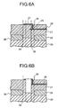
- Fig. 6A and Fig. 6B are vertical cross-sectional views of a portion cut along a B-B line of the semiconductor wafer shown in Fig. 5 .
- Fig. 6A shows a state before dicing
- Fig. 6B shows a state after dicing. Parts having structures identical to those of the first example are attached with the same reference numerals, and their explanation will be omitted.
- the second example is different from the first example in the following. That is, as shown in Fig. 5 , Fig. 6A, and Fig. 6B , and contact pads 29 and lead wires 28 connected to the pads 29 are formed on a wired layer which is below the layer on which the pads 22 are formed.
- the pads 22 are electrically connected to the pads 29 through contact sections 30 that pierce through an interlayer insulating film 27.
- the lead wires 28 are electrically connected to circuit elements of memory areas not shown.
- the lead wires 28 are made of tungsten, titanium, titanium nitride or copper.
- a method of manufacturing the semiconductor device according to the second example is different from that of the first example in that a multi-layer wiring technique is used to form wires.
- a multi-layer wiring technique is used to form wires.
- the wiring using the multi-layer wiring technique is not a gist of the present invention, this will not be explained here.
- the data-writing pads 22 are cut at the time of dicing in a similar manner to that of the first example. Accordingly, after the chip areas 21 have been cut and the IC chips are obtained, there remains almost no pad 22 or there remains no pad at all in the IC chips. Therefore, it is possible to prevent the write data from being read out from the memory areas of the IC chips and to prevent corruption of the written data.
- the lead wires 28 are formed on the wired layer of titanium nitride or copper.
- the structure is not limited to this.
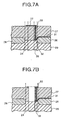
- lead wires 31 and contact pads 32 are continuously formed on a gate-wired layer as shown in Fig. 7A and Fig. 7B.
- Fig. 7A shows a state before dicing
- Fig. 7B shows a state after dicing.
- each pad 32 and each data-writing pad 22 are electrically connected with each other through a contact section 33 that pierces through an interlayer insulating film 27.
- the lead wires 31 are constructed of polysilicon, or by two layers of tungsten and polysilicon, or by tungsten.
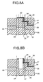
- lead wires 34 and 36 may be structured in a plurality of divided wired layers, as shown in Fig. 8A and Fig. 8B , for example.
- the lead wires 34 and contact pads 35 are formed continuously on a gate-wired layer made of polysilicon, for example.
- the lead wires 36 and contact pads 37 are continuously formed on a titanium nitride wired layer of an upper layer, for example.
- Fig. 8A shows a state before dicing
- Fig. 8B shows a state after dicing.
- each pad 35 and each upper-layer lead wire 36 are electrically connected with each other through a contact section 38 that pierces through the interlayer insulating film 27.
- each pad 37 and each data-writing pad 22 are electrically connected with each other through a contact section 39 that pierces through the interlayer insulating film 27.
- Fig. 9A, Fig. 9B , Fig. 10A, and Fig. 10B are vertical cross-sectional views of main portions of a semiconductor device illustrated in the order of manufacturing the device based on a manufacturing method relating to a third example which is not an embodiment of the present invention.
- chip areas 21, scribe areas 24, pads 22 and lead wires 23 are formed on a semiconductor substrate 20 (refer to Fig. 9A ). Data is written into memory areas not shown within the chip areas 21 through the pads 22. Then, a resist is coated onto the semiconductor substrate 20. Thereafter, light beams are irradiated onto the substrate after forming a mask.
- the irradiated surface is developed to expose the scribe areas 24 (refer to Fig. 9B ).
- the surface is then etched utilizing the remaining resist 40 as a mask, thereby removing the pads 22 on the scribe areas 24 (refer to Fig. 10A ).
- the wafer is cut to obtain the IC chips (refer to Fig. 10B ).
- the pads 22 are removed before dicing. Therefore, it is possible to prevent a part of the pad 22 from remaining in the IC chips after dicing when the width of the cut area 25 is smaller than the width of each pad 22. Therefore, after the wafer has been cut and the IC chips are obtained, it is possible to prevent the written data from being read out from the memory areas of the IC chips and to prevent corruption of the written data.
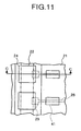
- Fig. 11 is a top plan view schematically illustrating an enlarged part of a scribe area of a semiconductor wafer manufactured by a method of a fourth example which is not an embodiment of the present invention.
- Fig. 12A and Fig. 12B are vertical cross-sectional invention.
- Fig. 12A and Fig. 12B are vertical cross-sectional views of a portion cut along a C-C line of the semiconductor wafer shown in Fig. 11 .
- Fig. 12A shows a state before dicing
- Fig. 12B shows a state after dicing.
- chip areas 21, scribe areas 24, data-writing pads 22, lead wires 28, contact pads 29, and contact sections 30 are formed on a semiconductor substrate 20. Further, fuse windows 41 are formed on the lead wires 28, based on a photolithographic technique or by etching, for example (refer to Fig. 11 and Fig. 12A ).
- the lead wires 28 are removed before dicing. Therefore, even if a part of the pad 22 remains in the IC chip after dicing, it is possible to isolate this pad from the inside memory area when the width of the cut area 25 is smaller than the width of each pad 22. Therefore, after the wafer has been cut and the IC chips are obtained, it is possible to prevent the written data from being read out from the memory areas of the IC chips and to prevent corruption of the written data.
- a MOS transistor 51 is provided in advance in the middle of each lead wire 28 within the chip area 21, as shown in Fig. 13 , and this transistor 51 is destroyed before dicing.
- a source and a drain of the MOS transistor 51 are connected to the data-writing pad 22 and the inside memory area respectively.
- a pad 52 for supplying a gate signal to the MOS transistor 51.
- a suitable gate signal is supplied from the outside to turn on the MOS transistor 51.
- a high voltage is applied to the pad 52, thereby destroying the transistor 51.
- the lead wire 28 is cut. Thereafter, dicing is carried out.
- another MOS transistor 53 may be formed between the MOS transistor 51 and the memory area, and the two MOS transistors 51 and 53 are connected in series.
- a pad 54 for supplying a gate signal to the MOS transistor 53.
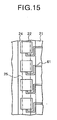
- Fig. 15 is a top plan view schematically illustrating an enlarged part of a scribe area of a semiconductor wafer manufactured by a method of a fifth example which is rot an embodiment of the present invention. Parts having the structures identical to those of the other examples are attached with the same reference numerals, and their explanation will be omitted.
- each lead wire 61 for electrically connecting each pad 22 with each memory area not shown within each chip area 21 is extended to surround the pad 22 by one quarter of the whole surrounding including one corner of the pad 22, and is connected to the pad 22 within the cut area 25. With this arrangement, the lead wire 61 is separated from the pad 22 at a connection portion.
- the lead wire 61 is cut in the middle by dicing. Therefore, even if a part of the pad 22 remains in the IC chip after dicing, it is possible to isolate this pad from the memory area. Accordingly, after the wafer has been cut and the IC chips are obtained, it is possible to prevent the written data from being read out from the memory areas of the IC chips and to prevent corruption of the written data.
- a lead wire 62 is extended to surround a pad 22 by one half of the whole surrounding across area 25, as shown in Fig. 16 .
- lead wires 63, 64 and 65 are extended in a length larger than the size of the pad 22 and turned within a scribe area 24 to exceed the cut area 25.
- Fig. 18 is a top plan view schematically illustrating an enlarged part of a scribe area of a semiconductor wafer manufactured by a method of a sixth example which is not an embodiment of the present invention. Parts having the structures identical to those of the other examples are attached with the same reference numerals, and their explanation will be omitted.
- pads 22a and 22b of adjacent chip areas 21a and 21b respectively are disposed within a scribe area 24 of both chip areas 21a and 21b.
- the pad 22a of one chip area 21a is disposed closer to the other chip area 21b.
- the pad 22b of the other chip area 21b is disposed closer to the other chip area 21a.
- the pads 22a and 22b are connected to memory areas within the respective chip areas 21a and 21b through lead wires 23a and 23b respectively.
- the pads 22a and 22b of the chip areas 21a and 21b are formed to extend over the cut area 25. Therefore, even if a part of the respective pads 22a and 22b remains in the IC chip after dicing, it is possible to isolate these pads from the respective memory areas as the respective pads were originally formed on the other IC chip. Accordingly, it is possible to prevent the write data from being read out from the memory areas of the IC chips and to prevent corruption of the written data.
- Fig. 19 is a top plan view schematically illustrating an enlarged part of a semiconductor wafer manufactured by a method of a seventh example which is not an embodiment of the present invention. Parts having the structures identical to those of the other examples are attached with the same reference numerals, and their explanation will be omitted.
- lead wires 71, 72, 73 and 74 for connecting pads 22 formed within a scribe area 24 to memory areas not shown within a chip area 21 are wired in a mutually insulated but complex and cris-crossed manner through a plurality of wired layers.
- the lead wires 71, 72, 73 and 74 that appear to be crossing when the chip area 21 is observed from the above are not actually in contact with each other as the lead wires 71, 72, 73 and 74 are formed on different levels of wired layers.
- the seventh example it is difficult to understand the wired routes of the lead wires 71, 72, 73 and 74 when the IC chip after dicing is observed from the above. Therefore, even if a part of the pad 22 remains after dicing, it is difficult to know which one of the pads is to be used to read the write data from the memory area within the IC chip. Accordingly, it is possible to prevent the written data from being read out from the memory areas of the IC chips and to prevent corruption of the written data from being.
- Fig. 20 is a top plan view schematically illustrating an enlarged part of a scribe area of a semiconductor wafer manufactured by a method of an embodiment of the present invention. Parts having the structures identical to those of the previously described examples are attached with the same reference numerals, and their explanation will be omitted.
- each pad 22 is formed within a chip area 21.
- a lead wire 81 electrically connected to a memory area not shown within the chip area 21 is extended to within a scribe area 24.
- the lead wire 81 is returned within the cut area 25 and is electrically connected to the pad 22 within the original chip area 21.
- the lead wire 81 is patterned to pass through the cut area 25. A part of the lead wire 81 is completely cut when the wafer is cut in the cut area 25 at the time of dicing.
- the pad 22 and the lead wire 81 may be formed on the same wired layer or on different wired layers, and they may be mutually electrically connected through a contact section.
- the lead wire 81 may extend over the cut area 25 and may be returned at an external portion of the cut area 25 within the scribe area 24.
- the lead wire 81 is cut in the middle at the time of dicing, it is possible to isolate the pad 22 from the memory area after dicing. Therefore, after the wafer has been cut and the IC chips are obtained, it is possible to prevent the written data from being read out from the memory areas of the IC chips and to prevent corruption of the written data.
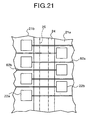
- Fig. 21 is a top plan view schematically illustrating an enlarged part of a scribe area of a semiconductor wafer manufactured by a method an eighth example which is not an embodiment of the present invention. Parts having the structures identical to those of the other examples are attached with the same reference numerals, and their explanation will be omitted.
- a lead wire connected to a memory area not shown within one chip area is extended over the cut area within a scribe area, and is electrically connected to a pad formed in another chip area.
- a pad 22a for writing data into a memory area not shown within one chip area 21a is formed within the other adjacent chip area 21b.
- a lead wire 82a extended from within one chip area 21a crosses the cut area 25 and is electrically connected to the pad 22a.
- a lead wire 82b extended from within the other chip area 21b crosses the cut area 25 and is electrically connected to the pad 22b.
- the two chip areas for forming pads are not limited to the adjacent chip areas.
- the pads 22a and 22b remain in the IC chip after dicing, these pads were originally formed in other IC chip. Therefore, it is possible to isolate these pads from the memory areas. Accordingly, after the wafer has been cut and the IC chips are obtained, it is possible to prevent the written data from being read out from the memory areas of the IC chips and to prevent corruption of the written data.
- pads for writing data into memory areas within chip areas are formed within the scribe areas. After the data has been written into the memory areas within the chip areas, the pads are cut together with the scribe areas when the wafer is diced. Therefore, after the wafer has been cut and the semiconductor chips are obtained, it is possible to prevent the written data from being read out from the memory areas of the semiconductor chips and to prevent corruption of the written data. Further, since the pads are formed in the scribe areas, it is possible to manufacture the chips in small sizes, which leads to a cost reduction.
- lead wires connected to pads are drawn out into the scribe areas.
- the lead wires are separated from the pads within the scribe areas, and parts of the wires are cut together with the scribe areas. Therefore, the lead wires are isolated from the pads, and they are electrically insulated. Accordingly, after the wafer has been cut and individual semiconductor chips are obtained, it is possible to prevent the written data from being read out from the memory areas of the semiconductor chips and to prevent corruption of the written data.
Landscapes
- Semiconductor Integrated Circuits (AREA)
- Semiconductor Memories (AREA)
- Dicing (AREA)
Description
- The present invention relates to a method of manufacturing a semiconductor device. More particularly this invention relates to a method of manufacturing a semiconductor device such as IC (integrated circuit) chips used for IC cards.
- It is expected in the future that there will be a wide distribution of IC cards such as, for example, railway ticket cards and electronic money cards in the field of electronic commerce. The IC cards are mounted with IC chips that store various kinds of information. The IC chips are generally constructed of nonvolatile memories, such as, for example, ferroelectric memories (FeRAM).
- Information about fare and a section of a railway a person travels, etc. are stored in the IC chips used as the railway ticket card. Information about a password, amount, a bank account number, a credit number, etc. is stored in IC chips used as the electronic money card. It is important that this information must not be made known to other persons, and that the information regarding money can not be rewritten by a third party.
- In general, a plurality of square chip areas, each chip area having a size of the order of a few millimeters on one side, are formed on a semiconductor wafer. The IC chips are then manufactured by cutting and separating these chip areas.
Fig. 1 is a top plan view schematically illustrating an enlarged main portion of a prior-art semiconductor wafer. A plurality ofchip areas 11 are formed on a semiconductor wafer 1. - Although not shown, circuit elements such as transistors are formed in each
chip area 11. A plurality ofpads 12 are also formed within eachchip area 11. Thepads 12 are electrically connected to various circuit elements withwires 13. Fourpads 12 are illustrated in this figure. However, in general, several to a hundredpads 12 are present in one wafer. - A
scribe area 14 is formed between thechip areas 11. The wafer 1 is cut along thescribe areas 14 using a diamond cutter or using laser beams at the time of dicing. Individual IC chips are obtained by such cutting. - In order to use these IC chips in the IC cards, it is necessary to write various information in a memory area within each chip before dicing, that is, when the IC chips are in the form of a wafer. As this information is extremely secret, it is necessary to provide various measures to prevent the information from being leaked to other persons or from being corrupted. Therefore, the technique of encryption or the like is utilized so as to prevent the written information from being easily stolen.
- When the conventional IC chips having a structure as shown in
Fig. 1 are to be used directly for IC cards, various pieces of secret information are written into the IC chips through thepads 12 before dicing. Accordingly, when IC cards mounted with the IC chips are handed over to users after dicing, there is a risk that the information written on the IC cards may be read out through thepads 12 that remain in thechip areas 11. Further, if a person succeeds in decoding the read out information, then he can easily corrupt the written information through the remainingpads 12. -
EP-A-0438 127 describes a semiconductor wafer, wherein upon the making of a die-sort testing for a predetermined IC pattern formed on each chip area; a plurality of sets of output pads selectively supplied with output signals are formed on the chip area and connected with a connection pattern on a dicing line area, and one testing pad is provided for the respective set of the pads. The IC patterns are tested by electrically contacting the testing pad with corresponding probe needle of probe card in a die-sort machine. -
WO 83/00244 - Embodiments of the present invention aim to provide a method of manufacturing a semiconductor device capable of preventing highly secret information written in the semiconductor device before dicing from being read out or corrupted after dicing.
- The invention is defined in the attached independent claim to which reference should now be made.
- The pads and the lead wires may be formed on the same metal wired layer. Alternatively, the pads and the lead wires may be formed on different wired layers, and they are electrically connected together through contact sections. Alternatively the lead wires may be formed on a plurality of divided wired layers, and the lead wires are electrically connected with the pads through contact sections.
- According to the invention, even if a part of the pad remains in the semiconductor chip after dicing, it is possible to isolate this pad from the inside memory area. Accordingly, after the semiconductor wafer has been disconnected to obtain the semiconductor chips, it is possible to prevent more securely the written data from being read out from the memory areas of the semiconductor chips and to prevent corruption of the written data.
- Based on the inventive method, a part of the lead wires is disconnected together with the scribe area at the time of dicing, so that the lead wires are separated from the pads. In other words, it is possible to electrically isolate the lead wires from the pads. Accordingly, after the semiconductor wafer has been cut and individual semiconductor chips are obtained, it is possible to prevent the written data from being read out from the memory areas of the semiconductor chips and to present corruption of the written data.
- A preferred embodiment of the present invention will now be described, by way of example only, with reference to the accompanying drawings, in which:
-
Fig. 1 is a top plan view schematically illustrating an enlarged main portion of a prior-art semiconductor wafer. -
Fig. 2 is a top plan view schematically illustrating an enlarged main portion of a semiconductor wafer manufactured by a method of a first example wich is not an embodiment of the present invention. -
Fig. 3 is a top plan view schematically illustrating an enlarged part of a scribe area of the semiconductor wafer shown inFig. 2 . -
Fig. 4A and Fig. 4B are vertical cross-sectional views of a portion cut along a line A-A of the semiconductor wafer shown inFig.3 . -
Fig. 5 is a top plan view schematically illustrating an enlarged part of a scribe area of a semiconductor wafer manufactured by a method of a second example which is not an embodiment of the present invention. -
Fig. 6A and Fig. 6B are vertical cross-sectional views of a portion cut along a B-B line of the semiconductor wafer shown inFig. 5 . -
Fig. 7A and Fig. 7B are vertical cross-sectional views illustrating a semiconductor wafer manufactured by a modification of the method of the second example. -
Fig. 8A and Fig. 8B are vertical cross-sectional views illustrating a semiconductor wafer manufactured by another modification of the method of the second example. -
Fig. 9A and Fig. 9B are vertical cross-sectional views of main portions of a semiconductor device illustrated in the order of manufacturing the device based on a manufacturing method relating to a third example which is not an embodiment of the present invention. -
Fig. 10A and Fig. 10B are vertical cross-sectional views of main portions of a semiconductor device illustrated in the order of manufacturing the device based on a manufacturing method relating to the third example. -
Fig. 11 is a top plan view schematically illustrating an enlarged part of a semiconductor wafer manufactured by a method of a fourth example which is not an embodiment of the present invention. -
Fig. 12A and Fig. 12B are vertical cross-sectional views of a portion cut along a C-C line of the semiconductor wafer shown inFig. 11 . -
Fig. 13 is a top plan view schematically illustrating a modification of the method of the fourth example. -
Fig. 14 is a top plan view schematically illustrating another modification of the method of the fourth example. -
Fig. 15 is a top plan view schematically illustrating an enlarged part of a scribe area of a semiconductor wafer manufactured by a method of a fifth example which is not an embodiment of the present invention. -
Fig. 16 is a top plan view schematically illustrating a modification of the method of the fifth example. -
Fig. 17 is a top plan view schematically illustrating another modification of the method of the fifth example. -
Fig. 18 is a top plan view schematically illustrating an enlarged part of a scribe area of a semiconductor wafer manufactured by a method of a sixth example which is not an embodiment of the present invention. -
Fig. 19 is a top plan view schematically illustrating an enlarged part of a semiconductor wafer manufactured by a method of a seventh example which is not an embodiment of the present invention. -
Fig. 20 is a top plan view schematically illustrating an enlarged part of a scribe area of a semiconductor wafer manufactured by a method of an embodiment of the present invention. -
Fig. 21 is a top plan view schematically illustrating an enlarged part of a scribe area of a semiconductor wafer manufactured by a method of an eighth example which is not an embodiment of the present invention. - Embodiments of a method of manufacturing a semiconductor device relating to the present invention will be explained in detail with reference to drawings.
-
Fig. 2 is a top plan view schematically illustrating an enlarged main portion of a semiconductor wafer manufactured using the method of a first example which is not an embodiment of the present invention.Fig. 3 is a top plan view schematically illustrating an enlarged part of a scribe area of the semiconductor wafer shown inFig. 2 .Fig. 4A and Fig. 4B are vertical cross-sectional views of a portion cut along a line A-A of the semiconductor wafer shown inFig.3 .Fig. 4A shows a state before dicing, andFig. 4B shows a state after dicing. - As shown in
Fig. 2 , a plurality ofchip areas 21 are formed on asemiconductor wafer 20. In eachchip area 21, there are formed circuit elements such as transistors (not shown). A memory area is constructed of the circuit elements. This memory area is used for storing encrypted secret information or the like. - A
scribe area 24 is formed betweenadjacent chip areas 21. A plurality ofpads 22 are formed in eachscribe area 24. Thepads 22 are used to supply electric signals from the outside at the time of writing information into the memory areas within thechip areas 21. In other words, thepads 22 are electrically connected to the circuit elements in the memory areas throughlead wires 23. Fourpads 22 are illustrated in this figure. However, in general, several to a hundred and dozens ofpads 22 are provided per chip. - At the time of dicing, the
semiconductor wafer 20 is cut along thescribe areas 24 using a diamond cutter or using laser beams. Individual IC chips are obtained after such cutting.Fig. 3 shows an area (hereinafter to be referred to as a cut area) 25 in which the IC chips are actually cut by dicing. - Each
pad 22 is disposed so that most (or all) of it is superimposed on thecut area 25. Accordingly, as shown inFig. 4B , most (or all) of eachpad 22 is cut out by dicing. In other words, in the IC chip obtained after dicing, almost no portion of the pad is left that can be used for reading out secret information stored in the memory area or for corrupting the secret information. - In the first example, the
pads 22 and thewires 23 are formed on the same wired layer, although there is no special limit to this arrangement. In other words, as shown inFig. 4A , aninterlayer insulating film 27 may be laminated on afield oxide film 26 which is laminated on a semiconductor substrate (or a semiconductor area) 20. Then, a wired layer may be laminated on this. Thepads 22 and thelead wires 23 are formed continuously on the wired layer. The wired layer is made of aluminum or copper, for example. - A method of manufacturing the semiconductor device according to the first example will be explained next. At first, the
field oxide film 26 is formed on thesemiconductor substrate 20 to divide the wafer into thechip areas 21 and thescribe areas 24. The circuit elements like transistors are formed within thechip areas 21. Then, theinterlayer insulating film 27 is laminated on thesemiconductor substrate 20. - Contact holes (not shown) are formed at predetermined portions of the
interlayer insulating film 27. The aluminum or copper wired layer is laminated on thesemiconductor substrate 20. This wired layer is patterned to form thepads 22 and thelead wires 23. Thus, thechip areas 21 have been formed. A state obtained by the above process is shown inFig. 4A . - The
pads 22 are disposed in thescribe areas 24. Thelead wires 23 are electrically connected to the circuit elements within thechip areas 21 through contact sections made of aluminum or copper filled in the contact holes. - Electric signals are supplied to the
pads 22 from the outside to write data into the memory areas within thechip areas 21. Thereafter, thesemiconductor substrate 20 is cut along thescribe areas 24 using a diamond cutter or using laser beams. When thesemiconductor substrate 20 is cut, thecut areas 25 within thescribe areas 24 are cut out. Thus, individual IC chips are obtained. A state obtained by the above process is shown inFig. 4B . - The IC chips obtained are packaged. Then, individual IC chips are mounted on cards having approximately a rectangular shape, thereby manufacturing the IC cards.
- According to the first example described above, the
pads 22 are formed in thescribe areas 24. Data is written into the memory areas within thechip areas 21 by using thepads 22. The wafer is diced to cut thepads 22 together with thescribe areas 24. Accordingly, after thechip areas 21 have been cut and the IC chips are obtained, there remains almost nopad 22 or there remains no pad at all in the IC chips. Therefore, it is possible to prevent the written data from being read out from the memory areas of the IC chips and to prevent corruption of the written data. -
Fig. 5 is a top plan view schematically illustrating an enlarged part of a scribe area of a semiconductor wafer manufactured using a method of a second example which is not an embodiment of the present invention.Fig. 6A and Fig. 6B are vertical cross-sectional views of a portion cut along a B-B line of the semiconductor wafer shown inFig. 5 .Fig. 6A shows a state before dicing, andFig. 6B shows a state after dicing. Parts having structures identical to those of the first example are attached with the same reference numerals, and their explanation will be omitted. - While the
lead wires 23 and thepads 22 are formed on the same wired layer in the first example, the second example is different from the first example in the following. That is, as shown inFig. 5 ,Fig. 6A, and Fig. 6B , andcontact pads 29 andlead wires 28 connected to thepads 29 are formed on a wired layer which is below the layer on which thepads 22 are formed. - The
pads 22 are electrically connected to thepads 29 throughcontact sections 30 that pierce through aninterlayer insulating film 27. Thelead wires 28 are electrically connected to circuit elements of memory areas not shown. Thelead wires 28 are made of tungsten, titanium, titanium nitride or copper. - A method of manufacturing the semiconductor device according to the second example is different from that of the first example in that a multi-layer wiring technique is used to form wires. However, as the wiring using the multi-layer wiring technique is not a gist of the present invention, this will not be explained here.
- According to the second example, the data-
writing pads 22 are cut at the time of dicing in a similar manner to that of the first example. Accordingly, after thechip areas 21 have been cut and the IC chips are obtained, there remains almost nopad 22 or there remains no pad at all in the IC chips. Therefore, it is possible to prevent the write data from being read out from the memory areas of the IC chips and to prevent corruption of the written data. - In the above-described second example , the
lead wires 28 are formed on the wired layer of titanium nitride or copper. However, the structure is not limited to this. For example, it is also possible to have such a structure that leadwires 31 andcontact pads 32 are continuously formed on a gate-wired layer as shown inFig. 7A and Fig. 7B. Fig. 7A shows a state before dicing, andFig. 7B shows a state after dicing. - In this case, each
pad 32 and each data-writing pad 22 are electrically connected with each other through acontact section 33 that pierces through aninterlayer insulating film 27. Thelead wires 31 are constructed of polysilicon, or by two layers of tungsten and polysilicon, or by tungsten. - Alternatively, lead
wires Fig. 8A and Fig. 8B , for example. Thelead wires 34 andcontact pads 35 are formed continuously on a gate-wired layer made of polysilicon, for example. Thelead wires 36 andcontact pads 37 are continuously formed on a titanium nitride wired layer of an upper layer, for example.Fig. 8A shows a state before dicing, andFig. 8B shows a state after dicing. - In this case, each
pad 35 and each upper-layer lead wire 36 are electrically connected with each other through acontact section 38 that pierces through theinterlayer insulating film 27. Further, eachpad 37 and each data-writing pad 22 are electrically connected with each other through acontact section 39 that pierces through theinterlayer insulating film 27. When thelead wires Fig. 8 , there is an advantage that it is difficult to understand the wired routes of thelead wires -
Fig. 9A, Fig. 9B ,Fig. 10A, and Fig. 10B are vertical cross-sectional views of main portions of a semiconductor device illustrated in the order of manufacturing the device based on a manufacturing method relating to a third example which is not an embodiment of the present invention. - According to the third example, in
Fig. 3 ,Fig. 4A, and Fig. 4B of the first example, for example, data is written into the memory areas within thechip areas 21, then thepads 22 are removed, and the wafer is diced thereafter. Parts having the structures identical to those of the first example are attached with the same reference numerals, and their explanation will be omitted. - At first,
chip areas 21,scribe areas 24,pads 22 andlead wires 23 are formed on a semiconductor substrate 20 (refer toFig. 9A ). Data is written into memory areas not shown within thechip areas 21 through thepads 22. Then, a resist is coated onto thesemiconductor substrate 20. Thereafter, light beams are irradiated onto the substrate after forming a mask. - Subsequently, the irradiated surface is developed to expose the scribe areas 24 (refer to
Fig. 9B ). The surface is then etched utilizing the remaining resist 40 as a mask, thereby removing thepads 22 on the scribe areas 24 (refer toFig. 10A ). Thereafter, the wafer is cut to obtain the IC chips (refer toFig. 10B ). - According to the third example, the
pads 22 are removed before dicing. Therefore, it is possible to prevent a part of thepad 22 from remaining in the IC chips after dicing when the width of thecut area 25 is smaller than the width of eachpad 22. Therefore, after the wafer has been cut and the IC chips are obtained, it is possible to prevent the written data from being read out from the memory areas of the IC chips and to prevent corruption of the written data. -
Fig. 11 is a top plan view schematically illustrating an enlarged part of a scribe area of a semiconductor wafer manufactured by a method of a fourth example which is not an embodiment of the present invention.Fig. 12A and Fig. 12B are vertical cross-sectional invention.Fig. 12A and Fig. 12B are vertical cross-sectional views of a portion cut along a C-C line of the semiconductor wafer shown inFig. 11 .Fig. 12A shows a state before dicing, andFig. 12B shows a state after dicing. - According to the fourth example, in
Fig. 5 ,Fig. 6A, and Fig. 6B of the second example, for example, data is written into the memory areas not shown within thechip areas 21, then thelead wires 28 are cut, and the wafer is diced thereafter. Parts having the structures identical to those of the second example are attached with the same reference numerals, and their explanation will be omitted. - At first,
chip areas 21,scribe areas 24, data-writing pads 22,lead wires 28,contact pads 29, andcontact sections 30 are formed on asemiconductor substrate 20. Further, fusewindows 41 are formed on thelead wires 28, based on a photolithographic technique or by etching, for example (refer toFig. 11 andFig. 12A ). - Then, data is written into memory areas not shown within the
chip areas 21 through thepads 22. Thereafter, laser beams are irradiated onto thefuse windows 41, thereby cutting thelead wires 28. Then, the wafer is diced to obtain IC chips (refer toFig. 12B ). - According to the fourth example, the
lead wires 28 are removed before dicing. Therefore, even if a part of thepad 22 remains in the IC chip after dicing, it is possible to isolate this pad from the inside memory area when the width of thecut area 25 is smaller than the width of eachpad 22. Therefore, after the wafer has been cut and the IC chips are obtained, it is possible to prevent the written data from being read out from the memory areas of the IC chips and to prevent corruption of the written data. - As a method of cutting the
lead wires 28, it may be so arranged that aMOS transistor 51 is provided in advance in the middle of eachlead wire 28 within thechip area 21, as shown inFig. 13 , and thistransistor 51 is destroyed before dicing. A source and a drain of theMOS transistor 51 are connected to the data-writing pad 22 and the inside memory area respectively. Further, inside thescribe area 24, there is formed apad 52 for supplying a gate signal to theMOS transistor 51. - At the time of writing data into each memory area, a suitable gate signal is supplied from the outside to turn on the
MOS transistor 51. After the data writing has been completed, a high voltage is applied to thepad 52, thereby destroying thetransistor 51. When eachtransistor 51 has been destroyed, thelead wire 28 is cut. Thereafter, dicing is carried out. - Further, as shown in
Fig. 14 , anotherMOS transistor 53 may be formed between theMOS transistor 51 and the memory area, and the twoMOS transistors scribe area 24, there is additionally formed apad 54 for supplying a gate signal to theMOS transistor 53. - At the time of writing data into each memory area, suitable gate signals are supplied from the outside to the two
MOS transistors MOS transistors transistor 53 at the memory area side is turned off, and then theother transistor 51 is destroyed. - With the above-described arrangement, it is possible to prevent the memory areas from being affected by the destruction of the
transistors 51. When all thetransistors 51 have been destroyed, thelead wires 28 are cut. The wafer is diced thereafter. -
Fig. 15 is a top plan view schematically illustrating an enlarged part of a scribe area of a semiconductor wafer manufactured by a method of a fifth example which is rot an embodiment of the present invention. Parts having the structures identical to those of the other examples are attached with the same reference numerals, and their explanation will be omitted. - In the fifth example, each
lead wire 61 for electrically connecting eachpad 22 with each memory area not shown within eachchip area 21 is extended to surround thepad 22 by one quarter of the whole surrounding including one corner of thepad 22, and is connected to thepad 22 within thecut area 25. With this arrangement, thelead wire 61 is separated from thepad 22 at a connection portion. - According to the fifth example, the
lead wire 61 is cut in the middle by dicing. Therefore, even if a part of thepad 22 remains in the IC chip after dicing, it is possible to isolate this pad from the memory area. Accordingly, after the wafer has been cut and the IC chips are obtained, it is possible to prevent the written data from being read out from the memory areas of the IC chips and to prevent corruption of the written data. - Further, in place of the
lead wire 61, alead wire 62 is extended to surround apad 22 by one half of the whole surrounding acrossarea 25, as shown inFig. 16 . Alternatively, as shown inFig. 17 ,lead wires pad 22 and turned within ascribe area 24 to exceed thecut area 25. - When the lead wires are arranged as shown in
Fig. 16 orFig. 17 , a part of thelead wires lead wires pads 22 respectively. Accordingly, even if a part of thepad 22 remains in the IC chip after dicing, it is possible to isolate this pad from the memory area. -
Fig. 18 is a top plan view schematically illustrating an enlarged part of a scribe area of a semiconductor wafer manufactured by a method of a sixth example which is not an embodiment of the present invention. Parts having the structures identical to those of the other examples are attached with the same reference numerals, and their explanation will be omitted. - In the sixth example,
pads adjacent chip areas scribe area 24 of bothchip areas - The
pad 22a of onechip area 21a is disposed closer to theother chip area 21b. Similarly, thepad 22b of theother chip area 21b is disposed closer to theother chip area 21a. Thepads respective chip areas lead wires - According to the sixth example , the
pads chip areas cut area 25. Therefore, even if a part of therespective pads -
Fig. 19 is a top plan view schematically illustrating an enlarged part of a semiconductor wafer manufactured by a method of a seventh example which is not an embodiment of the present invention. Parts having the structures identical to those of the other examples are attached with the same reference numerals, and their explanation will be omitted. - In the seventh
example lead wires pads 22 formed within ascribe area 24 to memory areas not shown within achip area 21 are wired in a mutually insulated but complex and cris-crossed manner through a plurality of wired layers. Thelead wires chip area 21 is observed from the above are not actually in contact with each other as thelead wires - According to the seventh example , it is difficult to understand the wired routes of the
lead wires pad 22 remains after dicing, it is difficult to know which one of the pads is to be used to read the write data from the memory area within the IC chip. Accordingly, it is possible to prevent the written data from being read out from the memory areas of the IC chips and to prevent corruption of the written data from being. -
Fig. 20 is a top plan view schematically illustrating an enlarged part of a scribe area of a semiconductor wafer manufactured by a method of an embodiment of the present invention. Parts having the structures identical to those of the previously described examples are attached with the same reference numerals, and their explanation will be omitted. - In the embodiment, each
pad 22 is formed within achip area 21. Alead wire 81 electrically connected to a memory area not shown within thechip area 21 is extended to within ascribe area 24. Thelead wire 81 is returned within thecut area 25 and is electrically connected to thepad 22 within theoriginal chip area 21. In other words, in the embodiment, thelead wire 81 is patterned to pass through thecut area 25. A part of thelead wire 81 is completely cut when the wafer is cut in thecut area 25 at the time of dicing. - The
pad 22 and thelead wire 81 may be formed on the same wired layer or on different wired layers, and they may be mutually electrically connected through a contact section. Alternatively, thelead wire 81 may extend over thecut area 25 and may be returned at an external portion of thecut area 25 within thescribe area 24. - According to the embodiment, as the
lead wire 81 is cut in the middle at the time of dicing, it is possible to isolate thepad 22 from the memory area after dicing. Therefore, after the wafer has been cut and the IC chips are obtained, it is possible to prevent the written data from being read out from the memory areas of the IC chips and to prevent corruption of the written data. -
Fig. 21 is a top plan view schematically illustrating an enlarged part of a scribe area of a semiconductor wafer manufactured by a method an eighth example which is not an embodiment of the present invention. Parts having the structures identical to those of the other examples are attached with the same reference numerals, and their explanation will be omitted. - In the eighth example, a lead wire connected to a memory area not shown within one chip area is extended over the cut area within a scribe area, and is electrically connected to a pad formed in another chip area. In the example shown in
Fig. 21 , in theadjacent chip areas pad 22a for writing data into a memory area not shown within onechip area 21a is formed within the otheradjacent chip area 21b. Then, alead wire 82a extended from within onechip area 21a crosses thecut area 25 and is electrically connected to thepad 22a. Similarly, alead wire 82b extended from within theother chip area 21b crosses thecut area 25 and is electrically connected to thepad 22b. The two chip areas for forming pads are not limited to the adjacent chip areas. - According to the eighth example, even if the
pads - According to the present invention, pads for writing data into memory areas within chip areas are formed within the scribe areas. After the data has been written into the memory areas within the chip areas, the pads are cut together with the scribe areas when the wafer is diced. Therefore, after the wafer has been cut and the semiconductor chips are obtained, it is possible to prevent the written data from being read out from the memory areas of the semiconductor chips and to prevent corruption of the written data. Further, since the pads are formed in the scribe areas, it is possible to manufacture the chips in small sizes, which leads to a cost reduction.
- Further, in accordance with one embodiment, lead wires connected to pads are drawn out into the scribe areas. The lead wires are separated from the pads within the scribe areas, and parts of the wires are cut together with the scribe areas. Therefore, the lead wires are isolated from the pads, and they are electrically insulated. Accordingly, after the wafer has been cut and individual semiconductor chips are obtained, it is possible to prevent the written data from being read out from the memory areas of the semiconductor chips and to prevent corruption of the written data.
- Although the invention has been described with respect to a specific embodiment for a complete and clear disclosure, the appended claims are not to be thus limited but are to be construed as embodying all modifications and alternative constructions that may occur to one skilled in the art which fairly fall within the basic teaching herein set forth.
Claims (1)
- A method of manufacturing a semiconductor device, the method comprising the steps of:forming a plurality of chip areas (21) having scribe areas (24) in between on a semiconductor wafer, the chip areas (21) including memory areas;forming pads (22) on the chip areas for writing data into the memory areas
wherein the method further includes providing lead wires (81), each connecting a memory area of a chip area to a pad formed on said chip area wherein a portion of each lead wire (81) is located within a cut area (25), the cut area (25) being a portion of the scribe area (24) where the semiconductor wafer is to be cut;writing data into the memory areas through the pads (22); andcutting the semiconductor wafer along the cut areas (25), within the scribe areas (24) after the data has been written, such that the lead wires (81) become electrically disconnected from the pads (22), thereby separating the chip areas (21) and obtaining semiconductor chips.
Priority Applications (1)
| Application Number | Priority Date | Filing Date | Title |
|---|---|---|---|
| EP07108693A EP1833086A3 (en) | 1999-08-26 | 2000-03-16 | A method of manufacturing a semiconductor device |
Applications Claiming Priority (4)
| Application Number | Priority Date | Filing Date | Title |
|---|---|---|---|
| JP24022799 | 1999-08-26 | ||
| JP24022799 | 1999-08-26 | ||
| JP2000038777A JP2001135597A (en) | 1999-08-26 | 2000-02-16 | Method for manufacturing semiconductor device |
| JP2000038777 | 2000-02-16 |
Related Child Applications (1)
| Application Number | Title | Priority Date | Filing Date |
|---|---|---|---|
| EP07108693A Division EP1833086A3 (en) | 1999-08-26 | 2000-03-16 | A method of manufacturing a semiconductor device |
Publications (3)
| Publication Number | Publication Date |
|---|---|
| EP1079430A2 EP1079430A2 (en) | 2001-02-28 |
| EP1079430A3 EP1079430A3 (en) | 2002-10-16 |
| EP1079430B1 true EP1079430B1 (en) | 2009-05-27 |
Family
ID=26534628
Family Applications (2)
| Application Number | Title | Priority Date | Filing Date |
|---|---|---|---|
| EP07108693A Withdrawn EP1833086A3 (en) | 1999-08-26 | 2000-03-16 | A method of manufacturing a semiconductor device |
| EP00302139A Expired - Lifetime EP1079430B1 (en) | 1999-08-26 | 2000-03-16 | A method of manufacturing a semiconductor device |
Family Applications Before (1)
| Application Number | Title | Priority Date | Filing Date |
|---|---|---|---|
| EP07108693A Withdrawn EP1833086A3 (en) | 1999-08-26 | 2000-03-16 | A method of manufacturing a semiconductor device |
Country Status (4)
| Country | Link |
|---|---|
| US (1) | US6365443B1 (en) |
| EP (2) | EP1833086A3 (en) |
| JP (1) | JP2001135597A (en) |
| DE (1) | DE60042254D1 (en) |
Families Citing this family (36)
| Publication number | Priority date | Publication date | Assignee | Title |
|---|---|---|---|---|
| JP3583662B2 (en) * | 1999-08-12 | 2004-11-04 | 株式会社 沖マイクロデザイン | Semiconductor device and method of manufacturing semiconductor device |
| US7678836B2 (en) * | 1999-11-04 | 2010-03-16 | Fxs Ventures, Llc | Method for rendering a contact lens wettable |
| US6730989B1 (en) * | 2000-06-16 | 2004-05-04 | Infineon Technologies Ag | Semiconductor package and method |
| US6815803B1 (en) | 2000-06-16 | 2004-11-09 | Infineon Technologies Ag | Multiple chip semiconductor arrangement having electrical components in separating regions |
| US6770544B2 (en) * | 2001-02-21 | 2004-08-03 | Nec Machinery Corporation | Substrate cutting method |
| JP3737405B2 (en) * | 2001-09-13 | 2006-01-18 | Necマイクロシステム株式会社 | Chip manufacturing method and system, circuit board, and circuit chip |
| US7183623B2 (en) * | 2001-10-02 | 2007-02-27 | Agere Systems Inc. | Trimmed integrated circuits with fuse circuits |
| US6759311B2 (en) * | 2001-10-31 | 2004-07-06 | Formfactor, Inc. | Fan out of interconnect elements attached to semiconductor wafer |
| JP4189902B2 (en) | 2002-02-06 | 2008-12-03 | 富士通株式会社 | Authentication circuit, semiconductor element and method of use thereof, and IC card and method of use thereof |
| US7259043B2 (en) * | 2002-05-14 | 2007-08-21 | Texas Instruments Incorporated | Circular test pads on scribe street area |
| US7026646B2 (en) | 2002-06-20 | 2006-04-11 | Micron Technology, Inc. | Isolation circuit |
| JP4405719B2 (en) * | 2002-10-17 | 2010-01-27 | 株式会社ルネサステクノロジ | Semiconductor wafer |
| US20060258135A1 (en) * | 2003-09-22 | 2006-11-16 | Matsushita Electtric Industrial Co., Ltd. | Semiconductor integrated circuit |
| JP4462903B2 (en) | 2003-11-18 | 2010-05-12 | パナソニック株式会社 | Semiconductor wafer |
| JP2005252196A (en) * | 2004-03-08 | 2005-09-15 | Toshiba Corp | Semiconductor device and manufacturing method thereof |
| DE102004014644A1 (en) * | 2004-03-25 | 2005-10-13 | Atmel Germany Gmbh | Integrated circuit |
| JP4595416B2 (en) * | 2004-07-15 | 2010-12-08 | ソニー株式会社 | Semiconductor wafer, semiconductor device, and manufacturing method of semiconductor device |
| FR2875624A1 (en) * | 2004-09-23 | 2006-03-24 | St Microelectronics Sa | DETERMINISTIC GENERATION OF AN IDENTIFIER NUMBER OF AN INTEGRATED CIRCUIT |
| JP2006140338A (en) * | 2004-11-12 | 2006-06-01 | Matsushita Electric Ind Co Ltd | Semiconductor device |
| US20060125508A1 (en) * | 2004-12-15 | 2006-06-15 | Impinj, Inc. | On wafer testing of RFID tag circuit with pseudo antenna signal |
| JP2006253402A (en) * | 2005-03-10 | 2006-09-21 | Nec Electronics Corp | Manufacturing method of semiconductor device |
| DE102005022600A1 (en) | 2005-05-10 | 2006-11-23 | Atmel Germany Gmbh | Integrated circuit with balancing elements and method of making the same |
| JP2006344795A (en) * | 2005-06-09 | 2006-12-21 | Disco Abrasive Syst Ltd | Wafer division method |
| JP4661383B2 (en) * | 2005-06-15 | 2011-03-30 | エプソントヨコム株式会社 | Method for manufacturing piezoelectric oscillator |
| KR100881108B1 (en) * | 2005-11-24 | 2009-02-02 | 가부시키가이샤 리코 | Semiconductor wafer comprising semiconductor chip partitioned by scribe lines and process-monitor electrode pads formed on scribe line |
| JP4861022B2 (en) | 2006-02-28 | 2012-01-25 | 富士通セミコンダクター株式会社 | Semiconductor device test circuit and test method, semiconductor wafer, and semiconductor chip manufacturing method |
| JP4907678B2 (en) * | 2009-02-20 | 2012-04-04 | ルネサスエレクトロニクス株式会社 | Manufacturing method of semiconductor device |
| ITMI20111418A1 (en) | 2011-07-28 | 2013-01-29 | St Microelectronics Srl | TESTING ARCHITECTURE OF CIRCUITS INTEGRATED ON A WAFER |
| US8552534B2 (en) * | 2011-11-01 | 2013-10-08 | Headway Technologies, Inc. | Laminated semiconductor substrate, semiconductor substrate, laminated chip package and method of manufacturing the same |
| US9508618B2 (en) * | 2014-04-11 | 2016-11-29 | Globalfoundries Inc. | Staggered electrical frame structures for frame area reduction |
| JP6558213B2 (en) | 2014-11-19 | 2019-08-14 | 株式会社デンソー | Manufacturing method of semiconductor wafer and semiconductor device |
| US10312091B1 (en) * | 2015-10-13 | 2019-06-04 | Multibeam Corporation | Secure permanent integrated circuit personalization |
| US10103116B2 (en) | 2016-02-01 | 2018-10-16 | Qualcomm Incorporated | Open-passivation ball grid array pads |
| DE102017207046B4 (en) * | 2017-04-26 | 2019-09-12 | Fraunhofer-Gesellschaft zur Förderung der angewandten Forschung e.V. | Method for producing and reading out a cryptographic circuit |
| US9818656B1 (en) * | 2017-05-23 | 2017-11-14 | Nxp Usa, Inc. | Devices and methods for testing integrated circuit devices |
| EP4734151A1 (en) * | 2024-10-22 | 2026-04-29 | Infineon Technologies Austria AG | Semiconductor chip, semiconductor wafer and method of fabricating a semiconductor chip |
Family Cites Families (15)
| Publication number | Priority date | Publication date | Assignee | Title |
|---|---|---|---|---|
| US4446475A (en) * | 1981-07-10 | 1984-05-01 | Motorola, Inc. | Means and method for disabling access to a memory |
| JPS59172243A (en) | 1983-03-18 | 1984-09-28 | Nippon Denso Co Ltd | Ic wafer |
| JPS60121599A (en) * | 1983-12-06 | 1985-06-29 | Fujitsu Ltd | integrated circuit device |
| JPS6187349A (en) | 1984-10-04 | 1986-05-02 | Nippon Denso Co Ltd | Semiconductor wafer |
| JPH0676000B2 (en) | 1985-09-30 | 1994-09-28 | カシオ計算機株式会社 | IC card manufacturing method |
| US4845351A (en) * | 1985-09-30 | 1989-07-04 | Casio Computer Co., Ltd. | IC card |
| JPH0758725B2 (en) * | 1990-01-19 | 1995-06-21 | 株式会社東芝 | Semiconductor wafer |
| US5059899A (en) * | 1990-08-16 | 1991-10-22 | Micron Technology, Inc. | Semiconductor dies and wafers and methods for making |
| DE69219165T2 (en) * | 1991-01-11 | 1997-08-07 | Texas Instruments Inc | Testing and baking system for a wafer and method for its manufacture |
| JPH0621188A (en) * | 1991-12-13 | 1994-01-28 | Yamaha Corp | Semiconductor wafer |
| JPH0737950A (en) * | 1993-07-20 | 1995-02-07 | Matsushita Electric Ind Co Ltd | Semiconductor device having circuit inspection pad |
| JPH07169807A (en) * | 1993-12-16 | 1995-07-04 | Nippondenso Co Ltd | Semiconductor wafer |
| JPH07302773A (en) * | 1994-05-06 | 1995-11-14 | Texas Instr Japan Ltd | Semiconductor wafer and semiconductor device |
| US5895942A (en) * | 1996-06-18 | 1999-04-20 | Kabushiki Kaisha Toshiba | Fuse selectable modules |
| JP3529581B2 (en) * | 1997-03-14 | 2004-05-24 | 東芝マイクロエレクトロニクス株式会社 | Semiconductor wafer and IC card |
-
2000
- 2000-02-16 JP JP2000038777A patent/JP2001135597A/en active Pending
- 2000-03-16 EP EP07108693A patent/EP1833086A3/en not_active Withdrawn
- 2000-03-16 EP EP00302139A patent/EP1079430B1/en not_active Expired - Lifetime
- 2000-03-16 DE DE60042254T patent/DE60042254D1/en not_active Expired - Lifetime
- 2000-03-30 US US09/538,231 patent/US6365443B1/en not_active Expired - Lifetime
Also Published As
| Publication number | Publication date |
|---|---|
| EP1079430A2 (en) | 2001-02-28 |
| EP1079430A3 (en) | 2002-10-16 |
| DE60042254D1 (en) | 2009-07-09 |
| EP1833086A2 (en) | 2007-09-12 |
| JP2001135597A (en) | 2001-05-18 |
| EP1833086A3 (en) | 2008-08-13 |
| US6365443B1 (en) | 2002-04-02 |
Similar Documents
| Publication | Publication Date | Title |
|---|---|---|
| US6365443B1 (en) | Method of manufacturing a semiconductor device having data pads formed in scribed area | |
| US5981971A (en) | Semiconductor ROM wafer test structure, and IC card | |
| US4446475A (en) | Means and method for disabling access to a memory | |
| KR100570241B1 (en) | Semiconductor integrated circuit device and manufacturing method thereof | |
| US7652363B2 (en) | Semiconductor device including an arrangement for detection of tampering | |
| KR20010046035A (en) | Architecture of LASER fuse box in semiconductor intergreated circuit device and method for fabricating the same | |
| CN102082145A (en) | Wafer and method for forming the same | |
| US6614080B2 (en) | Mask programmed ROM inviolable by reverse engineering inspections and method of fabrication | |
| JP4275110B2 (en) | Semiconductor device and IC card | |
| CN100555622C (en) | Semiconductor chip with identification code, manufacturing method and management system thereof | |
| KR100551932B1 (en) | Semiconductor memory device | |
| JP2520857B2 (en) | Integrated semiconductor circuit | |
| US20100193958A1 (en) | Semiconductor Device and a Method of Manufacturing the Same | |
| US6291844B1 (en) | Semiconductor memory device with an improved layout of programmable fuses | |
| JP2006344989A (en) | Manufacturing method of semiconductor device | |
| JP3670449B2 (en) | Semiconductor device | |
| JP3442994B2 (en) | Semiconductor device and manufacturing method thereof | |
| JP4386570B2 (en) | Safety integrated circuit device and manufacturing method thereof | |
| KR19980020175A (en) | A reel-type printed circuit board | |
| JP3383551B2 (en) | Semiconductor device and manufacturing method thereof | |
| JP3937813B2 (en) | Integrated circuit | |
| JP4246984B2 (en) | Manufacturing method of semiconductor device | |
| CN101083260A (en) | Semiconductor chip with die area | |
| JPS62160292A (en) | Card with built-in integrated circuit | |
| JPH11177024A (en) | Semiconductor device |
Legal Events
| Date | Code | Title | Description |
|---|---|---|---|
| PUAI | Public reference made under article 153(3) epc to a published international application that has entered the european phase |
Free format text: ORIGINAL CODE: 0009012 |
|
| AK | Designated contracting states |
Kind code of ref document: A2 Designated state(s): AT BE CH CY DE DK ES FI FR GB GR IE IT LI LU MC NL PT SE |
|
| AX | Request for extension of the european patent |
Free format text: AL;LT;LV;MK;RO;SI |
|
| PUAL | Search report despatched |
Free format text: ORIGINAL CODE: 0009013 |
|
| AK | Designated contracting states |
Kind code of ref document: A3 Designated state(s): AT BE CH CY DE DK ES FI FR GB GR IE IT LI LU MC NL PT SE |
|
| AX | Request for extension of the european patent |
Free format text: AL;LT;LV;MK;RO;SI |
|
| RIC1 | Information provided on ipc code assigned before grant |
Free format text: 7H 01L 21/82 A, 7H 01L 27/02 B, 7H 01L 23/58 B |
|
| 17P | Request for examination filed |
Effective date: 20021127 |
|
| AKX | Designation fees paid |
Designated state(s): DE FR GB |
|
| 17Q | First examination report despatched |
Effective date: 20051128 |
|
| GRAP | Despatch of communication of intention to grant a patent |
Free format text: ORIGINAL CODE: EPIDOSNIGR1 |
|
| GRAP | Despatch of communication of intention to grant a patent |
Free format text: ORIGINAL CODE: EPIDOSNIGR1 |
|
| RAP1 | Party data changed (applicant data changed or rights of an application transferred) |
Owner name: FUJITSU MICROELECTRONICS LIMITED |
|
| GRAS | Grant fee paid |
Free format text: ORIGINAL CODE: EPIDOSNIGR3 |
|
| GRAA | (expected) grant |
Free format text: ORIGINAL CODE: 0009210 |
|
| AK | Designated contracting states |
Kind code of ref document: B1 Designated state(s): DE FR GB |
|
| REG | Reference to a national code |
Ref country code: GB Ref legal event code: FG4D |
|
| REF | Corresponds to: |
Ref document number: 60042254 Country of ref document: DE Date of ref document: 20090709 Kind code of ref document: P |
|
| PLBE | No opposition filed within time limit |
Free format text: ORIGINAL CODE: 0009261 |
|
| STAA | Information on the status of an ep patent application or granted ep patent |
Free format text: STATUS: NO OPPOSITION FILED WITHIN TIME LIMIT |
|
| 26N | No opposition filed |
Effective date: 20100302 |
|
| GBPC | Gb: european patent ceased through non-payment of renewal fee |
Effective date: 20100316 |
|
| REG | Reference to a national code |
Ref country code: FR Ref legal event code: ST Effective date: 20101130 |
|
| PG25 | Lapsed in a contracting state [announced via postgrant information from national office to epo] |
Ref country code: FR Free format text: LAPSE BECAUSE OF NON-PAYMENT OF DUE FEES Effective date: 20100331 |
|
| PG25 | Lapsed in a contracting state [announced via postgrant information from national office to epo] |
Ref country code: GB Free format text: LAPSE BECAUSE OF NON-PAYMENT OF DUE FEES Effective date: 20100316 |
|
| PGFP | Annual fee paid to national office [announced via postgrant information from national office to epo] |
Ref country code: DE Payment date: 20170307 Year of fee payment: 18 |
|
| REG | Reference to a national code |
Ref country code: DE Ref legal event code: R119 Ref document number: 60042254 Country of ref document: DE |
|
| PG25 | Lapsed in a contracting state [announced via postgrant information from national office to epo] |
Ref country code: DE Free format text: LAPSE BECAUSE OF NON-PAYMENT OF DUE FEES Effective date: 20181002 |