EP1078459B1 - Device having a variable-speed motor - Google Patents
Device having a variable-speed motor Download PDFInfo
- Publication number
- EP1078459B1 EP1078459B1 EP00906250A EP00906250A EP1078459B1 EP 1078459 B1 EP1078459 B1 EP 1078459B1 EP 00906250 A EP00906250 A EP 00906250A EP 00906250 A EP00906250 A EP 00906250A EP 1078459 B1 EP1078459 B1 EP 1078459B1
- Authority
- EP
- European Patent Office
- Prior art keywords
- voltage
- motor
- switching means
- control
- coil arrangement
- Prior art date
- Legal status (The legal status is an assumption and is not a legal conclusion. Google has not performed a legal analysis and makes no representation as to the accuracy of the status listed.)
- Expired - Lifetime
Links
- 238000001208 nuclear magnetic resonance pulse sequence Methods 0.000 claims description 10
- 230000005669 field effect Effects 0.000 claims description 4
- 239000003990 capacitor Substances 0.000 description 21
- 229910005580 NiCd Inorganic materials 0.000 description 6
- 238000010276 construction Methods 0.000 description 6
- 125000004122 cyclic group Chemical group 0.000 description 5
- 238000000034 method Methods 0.000 description 5
- 230000008569 process Effects 0.000 description 5
- 230000009471 action Effects 0.000 description 4
- 230000003993 interaction Effects 0.000 description 4
- 230000007423 decrease Effects 0.000 description 3
- 230000000694 effects Effects 0.000 description 3
- 230000008878 coupling Effects 0.000 description 2
- 238000010168 coupling process Methods 0.000 description 2
- 238000005859 coupling reaction Methods 0.000 description 2
- 230000001052 transient effect Effects 0.000 description 2
- 230000032683 aging Effects 0.000 description 1
- 230000003247 decreasing effect Effects 0.000 description 1
- 238000010586 diagram Methods 0.000 description 1
- 230000002349 favourable effect Effects 0.000 description 1
- 230000001939 inductive effect Effects 0.000 description 1
Images

Classifications
-
- H—ELECTRICITY
- H03—ELECTRONIC CIRCUITRY
- H03K—PULSE TECHNIQUE
- H03K17/00—Electronic switching or gating, i.e. not by contact-making and –breaking
- H03K17/06—Modifications for ensuring a fully conducting state
- H03K17/063—Modifications for ensuring a fully conducting state in field-effect transistor switches
-
- H—ELECTRICITY
- H03—ELECTRONIC CIRCUITRY
- H03K—PULSE TECHNIQUE
- H03K17/00—Electronic switching or gating, i.e. not by contact-making and –breaking
- H03K17/51—Electronic switching or gating, i.e. not by contact-making and –breaking characterised by the components used
- H03K17/56—Electronic switching or gating, i.e. not by contact-making and –breaking characterised by the components used by the use, as active elements, of semiconductor devices
- H03K17/687—Electronic switching or gating, i.e. not by contact-making and –breaking characterised by the components used by the use, as active elements, of semiconductor devices the devices being field-effect transistors
Definitions
- the invention relates to a device as defined in the opening part of Claim 1.
- the known device includes two separate switching means, of which a first switching means serves for connecting and disconnecting the coil arrangement of the motor in a pulsating fashion for the purpose of influencing the speed of the motor and of which a second switching means serves for the purpose of producing turn-off voltage transients across the coil arrangement.
- the known device further includes a control pulse generator for each of the two switching means. Two such switching means and two such control pulse generators are comparatively expensive and further have the problem that an undesired interaction may occur between the processes caused by the switching means, which may lead to invalidation of the results of these processes.
- WO 99/30418 teaches a FET driver using inductive switching spikes from the inductance of the supply lead to boost the supply voltage to the driver.
- a device of the type defined in the opening sentence has the characteristic features defined in the characterizing part of Claim 1.
- the characteristic features provided in accordance with the invention result in a substantially simplified device in which an interaction between switching means is avoided and, consequently, no interactions between the processes caused by the switching means can occur, as a result of which the results of such processes cannot be invalidated.
- the single switching means may be constituted, for example, by a bipolar transistor, but when such a bipolar transistor is used care must be taken that the available d.c. supply voltage is at least a factor of ten (10) but preferably an even greater factor, as high as the saturation voltage of the bipolar transistor used, because otherwise a comparatively large portion of the energy provided by the d.c. supply voltage is transformed into heat. It has proved to be particularly advantageous if a device in accordance with the invention has the characteristic feature defined in Claim 2, because the construction of the single switching means as a field-effect transistor (FET) makes it possible to achieve an energy-saving and simple voltage supply to the control electrode.
- FET field-effect transistor
- the FET can be given a low turn-on resistance when the motor is connected to the d.c. supply voltage, which is of particular importance for the connection of a variable-speed motor to a d.c. supply voltage.
- a device in accordance with the invention can be operated with a d.c. supply voltage which is only slightly higher than the direct voltage required for controlling the control electrode of the single switching means.
- a variant of the device having the characteristic features defined in Claim 3 has proved to be particularly advantageous because a reliable starting of the motor is then even guaranteed if the value of the d.c. supply voltage available during operation is smaller than the minimum value of the control voltage required for the control electrode of the single switching means.
- the starting means may take the form of, for example, a wiper contact or a bipolar transistor.
- a wiper contact or a bipolar transistor.
- This measure guarantees a particularly reliable starting of the motor, starting being highly independent of aging as compared with a wiper contact.
- Figure 1 shows a device 1 having a motor 2.
- the motor 2 includes a coil arrangement 3 having two coil terminals 3a and 3b.
- the device 1 has two terminal means 4 and 5 arranged to receive a d.c. supply voltage V in operation, which voltage has a nominal value of 1.2 V in the present case.
- the first terminal means 4 of the device 1 has an electrically conductive connection to the first coil terminal 3a of the coil arrangement 3, as a result of which the d.c. supply voltage V is available across the coil arrangement 3.
- the device 1 further includes a circuit 6 adapted to power the motor 2.
- the source for the d.c. supply voltage V of the device 1 shown in Figure 1 takes the form of an external NiCd battery, which can be disconnected from and connected to the terminal means 4 and 5 of the device 1 by means of a switch 8.
- an NiCd battery 7 any other direct voltage source may be used in order to provide a d.c. supply voltage V.
- the d.c. supply voltage V may alternatively be applied to the terminal means 4 and 5 of the device 1 from a direct voltage source accommodated inside the device 1.
- the circuit 6 of the device 1 includes a switching means 9, which is advantageous formed by a field-effect transistor (FET) 9 and which has a first electrode D arranged in series with the second coil terminal 3b of the coil arrangement 3 and which, in its conductive state, enables an electrically conductive connection to be established between the second terminal means 5 and the second coil terminal 3b via a second electrode S.
- the switching means 9 has a control electrode G which serves for controlling the switching means 9.
- the switching means 9 serves both for connecting and disconnecting the coil arrangement 3 of the motor 2 to the d.c. supply voltage V in a pulsating fashion for the purpose of influencing the speed of the motor 2 and for producing turn-off voltage transients SP on the second coil terminal 3b of the coil arrangement 3 of the motor 2.
- the device 1 includes a control pulse generator 10 which is shown diagrammatically and of which only a transistor 11 at the output side and a collector resistance 12 connected to the collector electrode C of this transistor are shown.
- the control pulse generator 10 receives the d.c. supply voltage V when the switch 8 is closed.
- the emitter electrode E of the transistor 11 is connected to the second terminal means 5 of the device 1.
- the control pulse generator 10 is adapted to generate and supply a control pulse sequence Ci to the collector electrode C of the transistor 11. This control pulse sequence Ci can be applied to the control electrode G of the switching means 9 via a capacitor 13 and a circuit node A.
- a control pulse generator 10 which is typical of the device 1 as shown in Figure 1 takes the form of a constant-frequency astable multivibrator having means for duty cycle modulation.
- a control pulse generator may alternatively include a variable-frequency astable multivibrator.
- the output transistor 11 of the control pulse generator 10 is powered via a voltage boosting means 14 which precedes the collector resistor 12.
- the voltage boosting means 14 in the device 1 is formed by a series arrangement of a diode 15 and a parallel arrangement of a capacitor 16 and a zener diode 17.
- the voltage boosting means 14 has an input 18 connected to the anode of the diode 15, whose cathode is connected directly to an output 19 of the voltage boosting means 14.
- the input 15 of the voltage boosting means 14 is connected to the second coil terminal 3b and the first electrode D of the switching means 9.
- the device 1 further includes a starting means 20 comprising the capacitor 13 and a series arrangement of a resistor 21, a diode 22 and a further resistor 23, the capacitor 13 being connected to the node between the diode 22 and the resistor 23 and the further resistor 23 being connected to the second terminal means 5 of the device 1.
- a starting means 20 comprising the capacitor 13 and a series arrangement of a resistor 21, a diode 22 and a further resistor 23, the capacitor 13 being connected to the node between the diode 22 and the resistor 23 and the further resistor 23 being connected to the second terminal means 5 of the device 1.
- the device i.e. its circuit 2, further includes a means 24 for reducing the action time of the starting means 20.
- the means 24 comprises a capacitor 25 connected to the first terminal means 4 and, arranged in series with this capacitor, a resistor 26 connected to the second terminal means 5.
- a node B between the capacitor 25 and the resistor 26 is connected to the resistor 21 of the starting means 20 and is thus coupled to the starting means 20.
- the d.c. supply voltage V supplied by the NiCd battery 7 is applied to the device 1 via the two terminal means 4 and 5.
- the voltage appearing across the resistor 26 corresponds exactly to the d.c. supply voltage V at the closing instant of the switch 8 and decreases as an exponential function of time, which is defined by a time constant determined by the value of the resistor 26 and the value of the capacitor 25.
- the means 24 for reducing the action time of the starting means 20 and formed by the combination of the resistor 26 and the capacitor 25 is connected to the starting means 20 via the node B, as a result of which the voltage which appears on the node B and which decreases exponentially as a function of time is applied to the starting means 20 as a d.c. supply voltage which varies as a function of time, the action time of the starting means 20 being consequently dictated by the time characteristic of this voltage.
- the coil arrangement 3 of the motor 2 is also connected for the first time to the d.c. supply voltage V from the NiCd battery 7 via a current path which extends from the first terminal means 4 to the second terminal means 5 via the coil arrangement 3, the voltage boosting means 14, the resistor 12 and the transistor 11.
- the capacitor 13 is charged to a voltage value via the resistor 21 and the diode 22.
- a time constant determined by the combination of the capacitor 13 and the resistor 21 is small in comparison with the time constant determined by the combination of the capacitor 25 and the resistor 26 of the means 24. Furthermore, it is to be noted that the value of the resistor 23 of the starting means 20 is high in comparison with the value of the resistor 21 of the starting means 20. It has proved to be particularly advantageous to make the value of the resistor 21 so low that the control pulse generator 10 still starts in a reliable manner. Moreover, it is pointed out that in the case of an initial turn-on period of the transistor 11 shorter than the time constant defined by the capacitor 13 and the resistor 21 a voltage appears on the node which is smaller than the d.c. supply voltage V minus the voltage drop across the diode 22. Another effect which reduces the voltage across the capacitor 13 is obtained as a result of the variation in time of the voltage on the node B.
- the cyclic turn-off and turn-on of the transistor 11 causes a continual rise of the voltage on the node A in dependence on the turn-on/turn-off frequency and in dependence on the two above-mentioned time constants, which voltage is superimposed on the control pulse sequence Ci.
- the overall voltage on the node A assumes a value which is higher than the minimum value required for the d.c. control voltage for the control electrode G of the switching means 9, i.e. of the FET 9, to drive the switching means 9 into its conductive state.
- the starting means 20 is formed by a clamping circuit.
- the device 1 shown in Figure 1 uses a FET 9 for which the minimum d.c. control voltage required on the gate electrode G of the FET 9 to drive this FET into its conductive state is smaller than the maximum control voltage which can be generated on node A.
- Schottky diodes may be used for the diodes 15 and 22.
- the coil arrangement 3 of the motor 2 is for the first time connected to the d.c. supply voltage V via the internal resistance which then exists between the first electrode D and the second electrode S of the FET.
- the continued cyclic turn-on and turn-off of the transistor 11 causes a cyclic connection and disconnection of the coil arrangement 3 of the motor 2 to and from the d.c. supply voltage V and gives rise to a series of turn-off voltage transients SP on the second coil terminal 3b of the coil arrangement 3 of the motor 2.
- the turn-off voltage transients SP are applied to the capacitor 16 of the voltage boosting means 14 via the diode 15 and charge the capacitor 16, the maximum voltage which can build up on the output 19 of the voltage boosting means 14 being defined by the zener voltage of the zener diode 17 provided in the voltage boosting means 14. During each turn-on period of the transistor 11 the voltage which appears instantaneously across the capacitor 13 is added to the voltage which builds up on the output 19 of the voltage boosting means 14.
- the internal resistance of the FET 9 decreases as the voltage on the gate electrode G of the FET 9 increases, which voltage has been applied, via the collector electrode of the transistor 11, as the sum of the voltage on the output 19 of the voltage boosting means 14 and the instantaneous voltage across the capacitor 13 and reaches a minimum value when a nominal value is reached on the output 19 of the voltage boosting means 14.
- the starting means 20 has already lost most of its effect owing to the fact that the voltage on the node B has already decreased distinctly. This ensures that the minimum voltage of the control pulse sequence Ci appearing on the gate electrode G of the FET 9 during the turn-off period of the transistor 11 lies below the minimum value of the d.c. control voltage required on the gate electrode G of the FET 9 in order to drive the FET 9 into its conductive state, as a result of which a reliable turn-off of the FET 9 is guaranteed.
- the speed of the motor 2 is influenced, namely in that the coil arrangement 3 of the motor 2 is connected and disconnected in a pulsating fashion with the aid of the single switching means 9, i.e. the FET 9, the speed of the motor 2 being variable in a range from approximately 1 % to approximately 99 % of the maximum possible speed of the motor 2 by means of the single control pulse sequence Ci which can be supplied to the control electrode G of the single switching element 9 by the single control pulse generator 10.
- the single control pulse generator 10 is adapted to effect pulse width modulation, i.e. to influence the duty cycle of a constant-frequency control pulse sequence Ci.
- the duty cycle is influenced via a manual control by which the resistance value of a potentiometer, not shown in Figure 1 , of the control pulse generator 10.
- control pulse generator 10 is adapted to supply the control pulse sequence Ci for the connection and disconnection of the coil arrangement 3 in a pulsating fashion, i.e. for influencing the speed of the motor 2, and consequently the energization and de-energization of the coil arrangement 3 of the motor 2 for the purpose of generating turn-off transients SP used for powering the voltage boosting means are identical to the connection and disconnection of the coil arrangement 3, it is to be noted in this respect that the limits of the attainable speed variation of the motor 2 are dictated by the requirement of sustaining the output voltage on the output 19 of the voltage boosting means 14.
- the measures in accordance with the invention have resulted in a highly simplified construction. Since only a single switching means 9, namely the FET 9, has been provided for the connection and disconnection of the coil arrangement 3 of the motor 2 to and from the d.c. supply voltage V and for the energization and deenergization of the coil arrangement 3 of the motor 2, interaction between switching means is avoided and, as a consequence, processes caused by switching means cannot influence one another.
- the measures in accordance with the invention, particularly the provision of the voltage boosting means 14, enable the use of a comparatively favorable FET 9 in a standard version, which - if no voltage boosting means 14 had been provided - could only be used as a switching means 9 for influencing the speed of the motor 2 at a d.c. supply voltage V of at least 2. 5 V but which in the device 1 can be used correctly and without any problems in spite of the low d.c. supply voltage V of only 1.2 V for the device 1.
- the maximum voltage available on the output 19 of the voltage boosting means 14 is given by the nominal voltage of the zener diode 17, which is 6.8 V in the device shown information Figure 1 .
- the starting means 20 used in the device 1, which starting means has an action time limited by the means 24 and takes the form of a clamping circuit enables a reliable and dependable starting of the motor 2 for the given voltage values mentioned above.
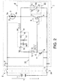
- FIG. 2 shows a second embodiment of a device 1 in accordance with the invention.
- This device 1 also includes a variable-speed motor 2 which has a coil arrangement 3 having two coil terminals 3a and 3b, a single control pulse generator 10, a voltage boosting means 14 and a starting means 20.
- the starting means 20 is realized by means of a switch 27 having a normally-closed contact Ta, a wiper contact Tb, a normally-open contact Tc and a fixed contact Td.
- the switch 27 of the starting means 20 is functionally coupled to the switch 8, as is shown by a dash-dot line 28 in Figure 2 .
- the motor 2 is started by actuation of the switch 8.
- the wiper contact Tb of the switch 27 is briefly connected to the fixed contact Td, after which the normally-open contact Tc is connected to the fixed contact Td.
- the coil arrangement 3 of the motor 2 is briefly connected to the d.c.
- the voltage on the output 19 of the starting means 14 appears on the collector electrode C of the control pulse generator 10 via the resistor 12 and is applied to the control electrode G of the single switching means 9 in the form of a control pulse sequence Ci.
- the subsequently continued cyclic turn-on and turn-off of the transistor 11 causes a cyclic connection and disconnection of the coil arrangement 3 of the motor 2 to and from the d.c. supply voltage V and thus the energization and deenergization of the coil arrangement 3 with the aid of the single switching means 9.
- the turn-off voltage transients SP generated upon the deenergization subsequently serve to build up a nominal output voltage on the output 19 of the voltage boosting means 14.
- an optimum conduction is achieved between the two terminals D and S of the single switching means 9.
- the implementation of the starting means 20 with the aid of the switch 27 results in a very robust and low-cost construction.
- the construction of the switch 27 as a printed circuit switch has proved to be very advantageous in view of the cost of the switch 27 and a good starting performance of the motor 2.
- the contact faces of the switch 27 are formed on a printed circuit board which also accommodates the circuit 6 and one switching contact of the switch 27 wipes over these contact faces on the printed circuit board.
- the wiper contact Tb takes the form of a series of separate contacts, as a result of which a series of turn-off voltage transients SP can be applied to the voltage boosting means 14 when the device 1 is put into operation by actuation of the switch 8 and, at the same time, the switch 27.
- a reliable starting of the motor 2 is achieved in a highly simple, robust, compact and cheap manner by the construction of the starting means 20 with the aid of the switch 27.
- the device 1 shown in Figure 2 also includes only one switching means 9 and one control pulse generator 10, which guarantees that also in this case the advantages of the device shown in Figure 1 are obtained.
Landscapes
- Control Of Direct Current Motors (AREA)
- Motor And Converter Starters (AREA)
- Electronic Switches (AREA)
- Dc-Dc Converters (AREA)
- Control Of Electric Motors In General (AREA)
- Control Of Stepping Motors (AREA)
Abstract
Description
- The invention relates to a device as defined in the opening part of
Claim 1. - Such a device of the type defined in the opening sentence is commercially available and frequently used in practice, and it is consequently known. For such a device reference can be made, for example, to the patent document
EP 0 222 042 A1 , Figure 3. - The known device includes two separate switching means, of which a first switching means serves for connecting and disconnecting the coil arrangement of the motor in a pulsating fashion for the purpose of influencing the speed of the motor and of which a second switching means serves for the purpose of producing turn-off voltage transients across the coil arrangement. The known device further includes a control pulse generator for each of the two switching means. Two such switching means and two such control pulse generators are comparatively expensive and further have the problem that an undesired interaction may occur between the processes caused by the switching means, which may lead to invalidation of the results of these processes.
WO 99/30418 - It is an object of the invention to improve a device of the type defined in the opening sentence and to provide an improved device having a simple construction, which precludes an invalidation of results by switching means, as is possible in a prior-art device.
- According to the invention, in order to achieve the afore-mentioned object, a device of the type defined in the opening sentence has the characteristic features defined in the characterizing part of
Claim 1. - The characteristic features provided in accordance with the invention result in a substantially simplified device in which an interaction between switching means is avoided and, consequently, no interactions between the processes caused by the switching means can occur, as a result of which the results of such processes cannot be invalidated.
- The single switching means may be constituted, for example, by a bipolar transistor, but when such a bipolar transistor is used care must be taken that the available d.c. supply voltage is at least a factor of ten (10) but preferably an even greater factor, as high as the saturation voltage of the bipolar transistor used, because otherwise a comparatively large portion of the energy provided by the d.c. supply voltage is transformed into heat. It has proved to be particularly advantageous if a device in accordance with the invention has the characteristic feature defined in Claim 2, because the construction of the single switching means as a field-effect transistor (FET) makes it possible to achieve an energy-saving and simple voltage supply to the control electrode. Moreover, by an appropriate dimensioning of the voltage boosting means the FET can be given a low turn-on resistance when the motor is connected to the d.c. supply voltage, which is of particular importance for the connection of a variable-speed motor to a d.c. supply voltage.
- A device in accordance with the invention can be operated with a d.c. supply voltage which is only slightly higher than the direct voltage required for controlling the control electrode of the single switching means. A variant of the device having the characteristic features defined in
Claim 3 has proved to be particularly advantageous because a reliable starting of the motor is then even guaranteed if the value of the d.c. supply voltage available during operation is smaller than the minimum value of the control voltage required for the control electrode of the single switching means. - The starting means may take the form of, for example, a wiper contact or a bipolar transistor. However, it has proved to be advantageous when the measure defined in Claim 4 is taken. This measure guarantees a particularly reliable starting of the motor, starting being highly independent of aging as compared with a wiper contact.
- For a highly reliable starting of the motor of the device in accordance with the invention the measure defined in
Claim 5 has proved to be very advantageous. The coupling of a timing means to the starting means constructed as a clamping circuit enables a well-controlled and efficient use of the clamping circuit. - The above-mentioned as well as further aspects of the invention will become apparent from the two examples embodiments described hereinafter and will be elucidated with reference to these examples.
- The invention will now be described in more detail with reference to the drawings, which shows two embodiments given by way of example but to which the invention is not limited.
-
Figure 1 shows diagrammatically and partly in the form of a block diagram a device in a first embodiment of the invention. -
Figure 2 shows, in the same way asFigure 1 , a device in a second embodiment of the invention. -
Figure 1 shows adevice 1 having a motor 2. The motor 2 includes acoil arrangement 3 having twocoil terminals device 1 has two terminal means 4 and 5 arranged to receive a d.c. supply voltage V in operation, which voltage has a nominal value of 1.2 V in the present case. The first terminal means 4 of thedevice 1 has an electrically conductive connection to thefirst coil terminal 3a of thecoil arrangement 3, as a result of which the d.c. supply voltage V is available across thecoil arrangement 3. - The
device 1 further includes a circuit 6 adapted to power the motor 2. It is to be noted that the source for the d.c. supply voltage V of thedevice 1 shown inFigure 1 takes the form of an external NiCd battery, which can be disconnected from and connected to the terminal means 4 and 5 of thedevice 1 by means of aswitch 8. It is to be noted that instead of an NiCd battery 7 any other direct voltage source may be used in order to provide a d.c. supply voltage V. Furthermore, it is to be noted that the d.c. supply voltage V may alternatively be applied to the terminal means 4 and 5 of thedevice 1 from a direct voltage source accommodated inside thedevice 1. - The circuit 6 of the
device 1 includes a switching means 9, which is advantageous formed by a field-effect transistor (FET) 9 and which has a first electrode D arranged in series with thesecond coil terminal 3b of thecoil arrangement 3 and which, in its conductive state, enables an electrically conductive connection to be established between the second terminal means 5 and thesecond coil terminal 3b via a second electrode S. The switching means 9 has a control electrode G which serves for controlling the switching means 9. The switching means 9 serves both for connecting and disconnecting thecoil arrangement 3 of the motor 2 to the d.c. supply voltage V in a pulsating fashion for the purpose of influencing the speed of the motor 2 and for producing turn-off voltage transients SP on thesecond coil terminal 3b of thecoil arrangement 3 of the motor 2. - The
device 1 includes acontrol pulse generator 10 which is shown diagrammatically and of which only atransistor 11 at the output side and acollector resistance 12 connected to the collector electrode C of this transistor are shown. Thecontrol pulse generator 10 receives the d.c. supply voltage V when theswitch 8 is closed. The emitter electrode E of thetransistor 11 is connected to the second terminal means 5 of thedevice 1. Thecontrol pulse generator 10 is adapted to generate and supply a control pulse sequence Ci to the collector electrode C of thetransistor 11. This control pulse sequence Ci can be applied to the control electrode G of the switching means 9 via acapacitor 13 and a circuit node A. It is to be noted that acontrol pulse generator 10 which is typical of thedevice 1 as shown inFigure 1 takes the form of a constant-frequency astable multivibrator having means for duty cycle modulation. However, such a control pulse generator may alternatively include a variable-frequency astable multivibrator. - The
output transistor 11 of thecontrol pulse generator 10 is powered via a voltage boosting means 14 which precedes thecollector resistor 12. The voltage boosting means 14 in thedevice 1 is formed by a series arrangement of adiode 15 and a parallel arrangement of acapacitor 16 and azener diode 17. The voltage boosting means 14 has aninput 18 connected to the anode of thediode 15, whose cathode is connected directly to anoutput 19 of the voltage boosting means 14. Theinput 15 of the voltage boosting means 14 is connected to thesecond coil terminal 3b and the first electrode D of the switching means 9. - The
device 1 further includes astarting means 20 comprising thecapacitor 13 and a series arrangement of aresistor 21, adiode 22 and afurther resistor 23, thecapacitor 13 being connected to the node between thediode 22 and theresistor 23 and thefurther resistor 23 being connected to the second terminal means 5 of thedevice 1. - The
device 1, i.e. its circuit 2, further includes ameans 24 for reducing the action time of thestarting means 20. Themeans 24 comprises acapacitor 25 connected to the first terminal means 4 and, arranged in series with this capacitor, aresistor 26 connected to the second terminal means 5. A node B between thecapacitor 25 and theresistor 26 is connected to theresistor 21 of the startingmeans 20 and is thus coupled to the startingmeans 20. - The operation of the circuit 6, and consequently of the
device 1, will be described in more detail hereinafter. - Upon closure of the
switch 8 the d.c. supply voltage V supplied by the NiCd battery 7 is applied to thedevice 1 via the two terminal means 4 and 5. The voltage appearing across theresistor 26 corresponds exactly to the d.c. supply voltage V at the closing instant of theswitch 8 and decreases as an exponential function of time, which is defined by a time constant determined by the value of theresistor 26 and the value of thecapacitor 25. The means 24 for reducing the action time of the starting means 20 and formed by the combination of theresistor 26 and thecapacitor 25 is connected to the starting means 20 via the node B, as a result of which the voltage which appears on the node B and which decreases exponentially as a function of time is applied to the starting means 20 as a d.c. supply voltage which varies as a function of time, the action time of the starting means 20 being consequently dictated by the time characteristic of this voltage. - At the instant at which the
switch 8 is closed for the first time and the d.c. supply voltage V is supplied from the NiCd battery 7 to thedevice 1 via the two terminal means 4 and 5 and at which thetransistor 11 of thecontrol pulse generator 10 is turned on by virtue of the operation of thecontrol pulse generator 10, thecoil arrangement 3 of the motor 2 is also connected for the first time to the d.c. supply voltage V from the NiCd battery 7 via a current path which extends from the first terminal means 4 to the second terminal means 5 via thecoil arrangement 3, thevoltage boosting means 14, theresistor 12 and thetransistor 11. In this state of the circuit thecapacitor 13 is charged to a voltage value via theresistor 21 and thediode 22. A time constant determined by the combination of thecapacitor 13 and theresistor 21 is small in comparison with the time constant determined by the combination of thecapacitor 25 and theresistor 26 of themeans 24. Furthermore, it is to be noted that the value of theresistor 23 of the starting means 20 is high in comparison with the value of theresistor 21 of the starting means 20. It has proved to be particularly advantageous to make the value of theresistor 21 so low that thecontrol pulse generator 10 still starts in a reliable manner. Moreover, it is pointed out that in the case of an initial turn-on period of thetransistor 11 shorter than the time constant defined by thecapacitor 13 and the resistor 21 a voltage appears on the node which is smaller than the d.c. supply voltage V minus the voltage drop across thediode 22. Another effect which reduces the voltage across thecapacitor 13 is obtained as a result of the variation in time of the voltage on the node B. - When the
transistor 11 is turned on for the first time under control of thecontrol pulse generator 10 thecoil arrangement 3 of the motor 2 is disconnected from the d.c. supply voltage V. On theoutput 19 of the voltage boosting means 14 a voltage is built up which corresponds to the d.c. supply voltage V minus the forward voltage of thediode 15. The interruption of the current flow through thetransistor 11 of thecontrol pulse generator 10 causes a voltage swing on the collector electrode C of thetransistor 11, which voltage swing corresponds to the voltage on theoutput 19 of thevoltage boosting means 14. As a result of this, the voltage which appears on the node A of the starting means 20 is also raised by the voltage drop across thecapacitor 13. Owing to the provision of thediode 22 and the high value of theresistor 23 in comparison with the value of he resistor 21 the charge of thecapacitor 13 remains substantially unchanged. Thus, after thetransistor 11 has been turned off and turned on for the first time it is achieved with the aid of the starting means 20 that on the control electrode G of the switching means 9 a voltage is obtained which corresponds to substantially twice the d.c. supply voltage V minus the voltage drops across thediodes - The cyclic turn-off and turn-on of the
transistor 11 causes a continual rise of the voltage on the node A in dependence on the turn-on/turn-off frequency and in dependence on the two above-mentioned time constants, which voltage is superimposed on the control pulse sequence Ci. Already after a few switching cycles of thetransistor 11, or more precisely during each turn-on period of thetransistor 11, the overall voltage on the node A assumes a value which is higher than the minimum value required for the d.c. control voltage for the control electrode G of the switching means 9, i.e. of theFET 9, to drive the switching means 9 into its conductive state. During each turn-off period of thetransistor 11 the minimum voltage appearing on the gate electrode G of theFET 9 is clamped by the voltage appearing across thecapacitor 20. Thus, the starting means 20 is formed by a clamping circuit. Furthermore, it is to be noted that thedevice 1 shown inFigure 1 uses aFET 9 for which the minimum d.c. control voltage required on the gate electrode G of theFET 9 to drive this FET into its conductive state is smaller than the maximum control voltage which can be generated on node A. Moreover, it is to be noted that in the case of an extremely low d.c. supply voltage V, as supplied by the NiCd battery 7 in thedevice 1 shown inFigure 1 , Schottky diodes may be used for thediodes - As soon as the voltage which appears on the node A, i.e. on the gate electrode G of the
FET 9 reaches a value at which theFET 9 is driven into its conductive state, thecoil arrangement 3 of the motor 2 is for the first time connected to the d.c. supply voltage V via the internal resistance which then exists between the first electrode D and the second electrode S of the FET. The continued cyclic turn-on and turn-off of thetransistor 11 causes a cyclic connection and disconnection of thecoil arrangement 3 of the motor 2 to and from the d.c. supply voltage V and gives rise to a series of turn-off voltage transients SP on thesecond coil terminal 3b of thecoil arrangement 3 of the motor 2. The turn-off voltage transients SP are applied to thecapacitor 16 of the voltage boosting means 14 via thediode 15 and charge thecapacitor 16, the maximum voltage which can build up on theoutput 19 of the voltage boosting means 14 being defined by the zener voltage of thezener diode 17 provided in thevoltage boosting means 14. During each turn-on period of thetransistor 11 the voltage which appears instantaneously across thecapacitor 13 is added to the voltage which builds up on theoutput 19 of thevoltage boosting means 14. The internal resistance of theFET 9 decreases as the voltage on the gate electrode G of theFET 9 increases, which voltage has been applied, via the collector electrode of thetransistor 11, as the sum of the voltage on theoutput 19 of thevoltage boosting means 14 and the instantaneous voltage across thecapacitor 13 and reaches a minimum value when a nominal value is reached on theoutput 19 of thevoltage boosting means 14. At this instant the starting means 20 has already lost most of its effect owing to the fact that the voltage on the node B has already decreased distinctly. This ensures that the minimum voltage of the control pulse sequence Ci appearing on the gate electrode G of theFET 9 during the turn-off period of thetransistor 11 lies below the minimum value of the d.c. control voltage required on the gate electrode G of theFET 9 in order to drive theFET 9 into its conductive state, as a result of which a reliable turn-off of theFET 9 is guaranteed. - During subsequent operation of the
device 1 the speed of the motor 2 is influenced, namely in that thecoil arrangement 3 of the motor 2 is connected and disconnected in a pulsating fashion with the aid of the single switching means 9, i.e. theFET 9, the speed of the motor 2 being variable in a range from approximately 1 % to approximately 99 % of the maximum possible speed of the motor 2 by means of the single control pulse sequence Ci which can be supplied to the control electrode G of thesingle switching element 9 by the singlecontrol pulse generator 10. In thedevice 1 shown inFigure 1 the singlecontrol pulse generator 10 is adapted to effect pulse width modulation, i.e. to influence the duty cycle of a constant-frequency control pulse sequence Ci. In thedevice 1 the duty cycle is influenced via a manual control by which the resistance value of a potentiometer, not shown inFigure 1 , of thecontrol pulse generator 10. - Since the
control pulse generator 10 is adapted to supply the control pulse sequence Ci for the connection and disconnection of thecoil arrangement 3 in a pulsating fashion, i.e. for influencing the speed of the motor 2, and consequently the energization and de-energization of thecoil arrangement 3 of the motor 2 for the purpose of generating turn-off transients SP used for powering the voltage boosting means are identical to the connection and disconnection of thecoil arrangement 3, it is to be noted in this respect that the limits of the attainable speed variation of the motor 2 are dictated by the requirement of sustaining the output voltage on theoutput 19 of thevoltage boosting means 14. - In the
device 1 the measures in accordance with the invention have resulted in a highly simplified construction. Since only a single switching means 9, namely theFET 9, has been provided for the connection and disconnection of thecoil arrangement 3 of the motor 2 to and from the d.c. supply voltage V and for the energization and deenergization of thecoil arrangement 3 of the motor 2, interaction between switching means is avoided and, as a consequence, processes caused by switching means cannot influence one another. Moreover, the measures in accordance with the invention, particularly the provision of thevoltage boosting means 14, enable the use of a comparativelyfavorable FET 9 in a standard version, which - if no voltage boosting means 14 had been provided - could only be used as a switching means 9 for influencing the speed of the motor 2 at a d.c. supply voltage V of at least 2. 5 V but which in thedevice 1 can be used correctly and without any problems in spite of the low d.c. supply voltage V of only 1.2 V for thedevice 1. The maximum voltage available on theoutput 19 of thevoltage boosting means 14 is given by the nominal voltage of thezener diode 17, which is 6.8 V in the device shown informationFigure 1 . In addition, the starting means 20 used in thedevice 1, which starting means has an action time limited by themeans 24 and takes the form of a clamping circuit, enables a reliable and dependable starting of the motor 2 for the given voltage values mentioned above. -
Figure 2 shows a second embodiment of adevice 1 in accordance with the invention. Thisdevice 1 also includes a variable-speed motor 2 which has acoil arrangement 3 having twocoil terminals control pulse generator 10, avoltage boosting means 14 and a starting means 20. However, in the present case the starting means 20 is realized by means of aswitch 27 having a normally-closed contact Ta, a wiper contact Tb, a normally-open contact Tc and a fixed contact Td. Theswitch 27 of the starting means 20 is functionally coupled to theswitch 8, as is shown by a dash-dot line 28 inFigure 2 . - In the
device 1 shown inFigure 2 the motor 2 is started by actuation of theswitch 8. By means of themechanical coupling 28 the wiper contact Tb of theswitch 27 is briefly connected to the fixed contact Td, after which the normally-open contact Tc is connected to the fixed contact Td. Owing to the temporary connection of the wiper contact Tb with the fixed contact Td thecoil arrangement 3 of the motor 2 is briefly connected to the d.c. supply voltage V, as a result of which a current flows through thecoil arrangement 3, after which the current flow through the coil arrangement 2 is interrupted and, consequently, a turn-off voltage transient SP is produced on thecoil terminal 3b, which transient is applied to the voltage boosting means 14 on whoseoutput 19 it produces for the first time a voltage having a higher value than the minimum value required for the d.c. control voltage for the control electrode G of the single switching means 9 to drive the switching means 9 into its conductive state, which switching means also takes the form of a field-effect transistor (FET) in the device shown informationFigure 2 . The voltage on theoutput 19 of the starting means 14 appears on the collector electrode C of thecontrol pulse generator 10 via theresistor 12 and is applied to the control electrode G of the single switching means 9 in the form of a control pulse sequence Ci. As already stated for thedevice 1 shown informationFigure 1 , the subsequently continued cyclic turn-on and turn-off of thetransistor 11 causes a cyclic connection and disconnection of thecoil arrangement 3 of the motor 2 to and from the d.c. supply voltage V and thus the energization and deenergization of thecoil arrangement 3 with the aid of the single switching means 9. The turn-off voltage transients SP generated upon the deenergization subsequently serve to build up a nominal output voltage on theoutput 19 of thevoltage boosting means 14. As a result of this, as already explained for thedevice 1 shown inFigure 1 , an optimum conduction is achieved between the two terminals D and S of the single switching means 9. - The implementation of the starting means 20 with the aid of the
switch 27 results in a very robust and low-cost construction. The construction of theswitch 27 as a printed circuit switch has proved to be very advantageous in view of the cost of theswitch 27 and a good starting performance of the motor 2. In this variant the contact faces of theswitch 27 are formed on a printed circuit board which also accommodates the circuit 6 and one switching contact of theswitch 27 wipes over these contact faces on the printed circuit board. In this variant it is very advantageous when the wiper contact Tb takes the form of a series of separate contacts, as a result of which a series of turn-off voltage transients SP can be applied to thevoltage boosting means 14 when thedevice 1 is put into operation by actuation of theswitch 8 and, at the same time, theswitch 27. Thus, a reliable starting of the motor 2 is achieved in a highly simple, robust, compact and cheap manner by the construction of the starting means 20 with the aid of theswitch 27. - In an advantageous manner the
device 1 shown inFigure 2 also includes only one switching means 9 and onecontrol pulse generator 10, which guarantees that also in this case the advantages of the device shown inFigure 1 are obtained.
Claims (5)
- A device (1) comprising:a motor (2) having a coil arrangement (3),a circuit (6) for powering the motor (2) by energization and deenergization in a pulsating fashion to influence a speed of the motor (2),two terminal means (4, 5) arranged to receive a d.c. supply voltage (V) in operation,a single switching means (9) arranged in series with the motor (2) and having a control electrode (G), which switching means serves for: (i) the connection and disconnection of the coil arrangement (3) of the motor (2) to and from the d.c. supply voltage (V) in a pulsating fashion for the purpose of influencing the speed of the motor (2), and (ii) the energization and deenergization of the coil arrangement (3) and consequently producing turn-off voltage transients (SP) on a coil terminal (3b) of the coil arrangement (3), wherein the coil terminal (3b) is a junction between the motor (2) and the switching means (9),a control pulse generator (10) for generating and supplying a control pulse sequence (Ci) to the control electrode (G) of the switching means (9) which serves for the connection and disconnection of the coil arrangement (3), and for the energization and deenergization of the coil arrangement (3), andvoltage boosting means (14) for receiving the turn-off voltage transients (SP) on the junction and for generating a d.c. control voltage in dependence on the turn-off voltage transients (SP) and for supplying the generated d.c. control voltage to the switching means (9) which serves for the connection and disconnection of the coil arrangement (3), andwherein the d.c. control voltage from the voltage boosting means (14) and the control pulse sequence (Ci) from the control pulse generator (10), in operation, are applied to said control electrode (G), and the connection and disconnection of the coil arrangement (3) and the energization and deenergization of said coil arrangement are identical.
- A device (1) as claimed in Claim 1, characterized in that the single switching means (9) is formed by a field-effect transistor (9).
- A device (1) as claimed in Claim 1 or 2, characterized in that the device (1) is adapted to operate at a d.c. supply voltage (V) whose value is smaller than the minimum value required for the d.c. control voltage for the control electrode (G) of the single switching means (9) to drive the single switching means (9) into its conductive state, and a starting means (20) has been provided by which a minimum d.c. control voltage required for the control electrode (G) of the single switching means (9) in order to drive the single switching means (9) into its conductive state can be built up for a first time.
- A device (1) as claimed in Claim 3, characterized in that the starting means (20) is formed by a clamping circuit arranged before the control electrode (G) of the single switching means (9).
- A device (1) as claimed in Claim 4, characterized in that the starting means (20) is coupled to a means (24) for making reducing the time during which the starting means (20) is active by a given time interval.
Priority Applications (1)
| Application Number | Priority Date | Filing Date | Title |
|---|---|---|---|
| EP00906250A EP1078459B1 (en) | 1999-03-01 | 2000-01-31 | Device having a variable-speed motor |
Applications Claiming Priority (4)
| Application Number | Priority Date | Filing Date | Title |
|---|---|---|---|
| EP99890069 | 1999-03-01 | ||
| EP99890069 | 1999-03-01 | ||
| PCT/EP2000/000742 WO2000052823A1 (en) | 1999-03-01 | 2000-01-31 | Device having a variable-speed motor |
| EP00906250A EP1078459B1 (en) | 1999-03-01 | 2000-01-31 | Device having a variable-speed motor |
Publications (2)
| Publication Number | Publication Date |
|---|---|
| EP1078459A1 EP1078459A1 (en) | 2001-02-28 |
| EP1078459B1 true EP1078459B1 (en) | 2009-03-11 |
Family
ID=8243962
Family Applications (1)
| Application Number | Title | Priority Date | Filing Date |
|---|---|---|---|
| EP00906250A Expired - Lifetime EP1078459B1 (en) | 1999-03-01 | 2000-01-31 | Device having a variable-speed motor |
Country Status (7)
| Country | Link |
|---|---|
| US (1) | US6310449B1 (en) |
| EP (1) | EP1078459B1 (en) |
| JP (1) | JP4597381B2 (en) |
| CN (1) | CN1162971C (en) |
| AT (1) | ATE425584T1 (en) |
| DE (1) | DE60041743D1 (en) |
| WO (1) | WO2000052823A1 (en) |
Families Citing this family (9)
| Publication number | Priority date | Publication date | Assignee | Title |
|---|---|---|---|---|
| KR100417116B1 (en) * | 2002-02-19 | 2004-02-05 | 디알에스테크 주식회사 | A power supply of wiper for a railway vehicle |
| US8618805B2 (en) * | 2004-03-25 | 2013-12-31 | 02Micro, Inc. | Battery pack with a battery protection circuit |
| US7589499B2 (en) * | 2004-03-25 | 2009-09-15 | O2Micro International Limited | Over voltage transient controller |
| NL1029586C2 (en) * | 2005-07-22 | 2007-01-23 | Electrische App Nfabriek Capax | Control circuit for DC motor power supply, used for battery driven electric hand tools, includes semiconductor switch with anti parallel zener diode |
| WO2010034162A1 (en) * | 2008-09-28 | 2010-04-01 | Bosch Power Tools (China) Co., Ltd. | Control device for controlling a motor in a low voltage dc power tool and control method thereof |
| EP2571150A3 (en) * | 2011-09-16 | 2018-02-28 | Braun GmbH | Power-supply circuit for an electrical appliance having a battery and a dc-to-dc converter |
| TW201345780A (en) * | 2012-05-08 | 2013-11-16 | Univ Nat Chiao Tung | Embedded industrial controller with bicycle frame shape |
| US9531373B2 (en) | 2013-07-04 | 2016-12-27 | Nxp Usa, Inc. | Gate drive circuit and a method for setting up a gate drive circuit |
| US12476569B2 (en) | 2020-12-11 | 2025-11-18 | Snap-On Incorporated | Tool brownout management |
Family Cites Families (15)
| Publication number | Priority date | Publication date | Assignee | Title |
|---|---|---|---|---|
| JPS6042715B2 (en) * | 1980-12-10 | 1985-09-24 | 三洋電機株式会社 | Motor control method |
| GB2114323B (en) * | 1981-10-15 | 1985-06-26 | Univ Dundee | Automatic control of d.c motors |
| EP0222042A1 (en) | 1985-11-15 | 1987-05-20 | Deutsche ITT Industries GmbH | Circuit arrangement of an isolation layer field effect transistor and a coil |
| US4774624A (en) * | 1987-07-06 | 1988-09-27 | Motorola, Inc. | Boost voltage power supply for vehicle control system |
| JP2773476B2 (en) * | 1991-07-23 | 1998-07-09 | 日産自動車株式会社 | Load control power supply |
| JPH05146190A (en) * | 1991-11-20 | 1993-06-11 | Makita Corp | Speed controller for dc motor |
| DE4325899C2 (en) * | 1993-08-02 | 1995-11-16 | Siemens Ag | MOS switching stage |
| CN1050576C (en) * | 1993-09-14 | 2000-03-22 | 株式会社利肯 | electric bicycle |
| JP3325697B2 (en) * | 1994-01-20 | 2002-09-17 | 三菱電機株式会社 | Power device control device and motor drive control device |
| JP3003399U (en) * | 1994-04-21 | 1994-10-18 | 船井電機株式会社 | Motor drive circuit powered by batteries |
| DE69535329T2 (en) * | 1994-05-12 | 2007-04-05 | Komatsu Ltd. | LAST DRIVER DEVICE |
| JPH0833314A (en) * | 1994-05-12 | 1996-02-02 | Komatsu Ltd | Load drive |
| JP3067601B2 (en) * | 1995-08-02 | 2000-07-17 | 株式会社デンソー | Electric motor control device |
| JPH11113283A (en) * | 1997-09-30 | 1999-04-23 | Toshiba Corp | Motor drive |
| DE19754574A1 (en) * | 1997-12-09 | 1999-06-10 | Mannesmann Vdo Ag | Circuit arrangement for clocked control of a load |
-
2000
- 2000-01-31 AT AT00906250T patent/ATE425584T1/en not_active IP Right Cessation
- 2000-01-31 DE DE60041743T patent/DE60041743D1/en not_active Expired - Lifetime
- 2000-01-31 WO PCT/EP2000/000742 patent/WO2000052823A1/en not_active Ceased
- 2000-01-31 EP EP00906250A patent/EP1078459B1/en not_active Expired - Lifetime
- 2000-01-31 JP JP2000603147A patent/JP4597381B2/en not_active Expired - Fee Related
- 2000-01-31 CN CNB008002061A patent/CN1162971C/en not_active Expired - Fee Related
- 2000-02-28 US US09/514,173 patent/US6310449B1/en not_active Expired - Fee Related
Also Published As
| Publication number | Publication date |
|---|---|
| DE60041743D1 (en) | 2009-04-23 |
| CN1162971C (en) | 2004-08-18 |
| JP4597381B2 (en) | 2010-12-15 |
| US6310449B1 (en) | 2001-10-30 |
| CN1297612A (en) | 2001-05-30 |
| EP1078459A1 (en) | 2001-02-28 |
| WO2000052823A1 (en) | 2000-09-08 |
| ATE425584T1 (en) | 2009-03-15 |
| JP2002538708A (en) | 2002-11-12 |
Similar Documents
| Publication | Publication Date | Title |
|---|---|---|
| US5479089A (en) | Power converter apparatus having instantaneous commutation switching system | |
| US4878147A (en) | Electromagnetic coil drive device | |
| EP0763882B1 (en) | Load driving device | |
| US11894657B2 (en) | Pulse generator circuit, related system and method | |
| US6310449B1 (en) | Device having a variable-speed motor | |
| EP0726394B1 (en) | A power supply for vibrating compressors | |
| JP3298624B2 (en) | Switching power supply | |
| US6559625B2 (en) | Circuit arrangement and electrical appliance with an inductive load and a buck converter | |
| CN206041860U (en) | Motor drive device | |
| RU2187161C2 (en) | Device controlling electromagnet | |
| JPH10248256A (en) | Switching power-supply apparatus with electricity-saving function | |
| US6016261A (en) | Switching voltage converter with synchronous rectification | |
| JP2507147B2 (en) | Strobe device | |
| US20220205305A1 (en) | Automatic door operator and method for driving the same | |
| JPH08107669A (en) | Step-up chopper regulator | |
| CN116331059B (en) | Battery connectors and vehicle battery systems | |
| JP3963590B2 (en) | Power supply | |
| CN215679105U (en) | Intelligent switch and intelligent household electrical appliance | |
| CN110324028A (en) | Control device for power semiconductor switch | |
| JP2003500990A (en) | Method for controlling at least one inductive load using a pulse width modulated control signal | |
| CN101277090A (en) | Insulation triggering circuit for vehicle magnetoelectric generator controlled rectifier | |
| JP2001340276A (en) | Electric vacuum cleaner | |
| JPS61142963A (en) | power supply | |
| SU1683164A1 (en) | Dc electric drive | |
| JPH0717274Y2 (en) | Self-excited DC / DC converter |
Legal Events
| Date | Code | Title | Description |
|---|---|---|---|
| PUAI | Public reference made under article 153(3) epc to a published international application that has entered the european phase |
Free format text: ORIGINAL CODE: 0009012 |
|
| AK | Designated contracting states |
Kind code of ref document: A1 Designated state(s): AT BE CH CY DE DK ES FI FR GB GR IE IT LI LU MC NL PT SE |
|
| 17P | Request for examination filed |
Effective date: 20010308 |
|
| RBV | Designated contracting states (corrected) |
Designated state(s): AT DE ES FR GB IT |
|
| 17Q | First examination report despatched |
Effective date: 20070817 |
|
| GRAP | Despatch of communication of intention to grant a patent |
Free format text: ORIGINAL CODE: EPIDOSNIGR1 |
|
| GRAS | Grant fee paid |
Free format text: ORIGINAL CODE: EPIDOSNIGR3 |
|
| GRAA | (expected) grant |
Free format text: ORIGINAL CODE: 0009210 |
|
| AK | Designated contracting states |
Kind code of ref document: B1 Designated state(s): AT DE ES FR GB IT |
|
| REG | Reference to a national code |
Ref country code: GB Ref legal event code: FG4D |
|
| REF | Corresponds to: |
Ref document number: 60041743 Country of ref document: DE Date of ref document: 20090423 Kind code of ref document: P |
|
| PG25 | Lapsed in a contracting state [announced via postgrant information from national office to epo] |
Ref country code: AT Free format text: LAPSE BECAUSE OF FAILURE TO SUBMIT A TRANSLATION OF THE DESCRIPTION OR TO PAY THE FEE WITHIN THE PRESCRIBED TIME-LIMIT Effective date: 20090311 |
|
| PG25 | Lapsed in a contracting state [announced via postgrant information from national office to epo] |
Ref country code: ES Free format text: LAPSE BECAUSE OF FAILURE TO SUBMIT A TRANSLATION OF THE DESCRIPTION OR TO PAY THE FEE WITHIN THE PRESCRIBED TIME-LIMIT Effective date: 20090622 |
|
| PLBE | No opposition filed within time limit |
Free format text: ORIGINAL CODE: 0009261 |
|
| STAA | Information on the status of an ep patent application or granted ep patent |
Free format text: STATUS: NO OPPOSITION FILED WITHIN TIME LIMIT |
|
| 26N | No opposition filed |
Effective date: 20091214 |
|
| PG25 | Lapsed in a contracting state [announced via postgrant information from national office to epo] |
Ref country code: IT Free format text: LAPSE BECAUSE OF FAILURE TO SUBMIT A TRANSLATION OF THE DESCRIPTION OR TO PAY THE FEE WITHIN THE PRESCRIBED TIME-LIMIT Effective date: 20090311 |
|
| PGFP | Annual fee paid to national office [announced via postgrant information from national office to epo] |
Ref country code: DE Payment date: 20120402 Year of fee payment: 13 |
|
| PGFP | Annual fee paid to national office [announced via postgrant information from national office to epo] |
Ref country code: GB Payment date: 20130201 Year of fee payment: 14 Ref country code: FR Payment date: 20130219 Year of fee payment: 14 |
|
| PG25 | Lapsed in a contracting state [announced via postgrant information from national office to epo] |
Ref country code: DE Free format text: LAPSE BECAUSE OF NON-PAYMENT OF DUE FEES Effective date: 20130801 |
|
| REG | Reference to a national code |
Ref country code: DE Ref legal event code: R119 Ref document number: 60041743 Country of ref document: DE Effective date: 20130801 |
|
| GBPC | Gb: european patent ceased through non-payment of renewal fee |
Effective date: 20140131 |
|
| REG | Reference to a national code |
Ref country code: FR Ref legal event code: ST Effective date: 20140930 |
|
| PG25 | Lapsed in a contracting state [announced via postgrant information from national office to epo] |
Ref country code: GB Free format text: LAPSE BECAUSE OF NON-PAYMENT OF DUE FEES Effective date: 20140131 Ref country code: FR Free format text: LAPSE BECAUSE OF NON-PAYMENT OF DUE FEES Effective date: 20140131 |