JP3963590B2 - Power supply - Google Patents
Power supply Download PDFInfo
- Publication number
- JP3963590B2 JP3963590B2 JP26418298A JP26418298A JP3963590B2 JP 3963590 B2 JP3963590 B2 JP 3963590B2 JP 26418298 A JP26418298 A JP 26418298A JP 26418298 A JP26418298 A JP 26418298A JP 3963590 B2 JP3963590 B2 JP 3963590B2
- Authority
- JP
- Japan
- Prior art keywords
- voltage
- terminal
- coil
- output
- level
- Prior art date
- Legal status (The legal status is an assumption and is not a legal conclusion. Google has not performed a legal analysis and makes no representation as to the accuracy of the status listed.)
- Expired - Fee Related
Links
Images


Description
【0001】
【発明の属する技術分野】
本発明は、入力電圧をチョッパ方式により所定の電圧に変換して出力する電源装置に関し、より詳しくは、降圧用同期整流回路と昇降圧用回路の機能を兼ね備えた電源装置に関する。
【0002】
【従来の技術】
所定電圧よりも高い入力電圧を効率よく所定電圧まで下降させるチョッパ方式の同期整流回路と、所定電圧よりも低い入力電圧を所定電圧まで上昇させ、所定電圧よりも高い入力電圧を所定電圧まで下降させる、同じくチョッパ方式の昇降圧用回路がある。従来の降圧用同期整流回路と昇降圧用回路の構成をそれぞれ図6および7に示す。
【0003】
図6の降圧用同期整流回路6は、入力端子51と出力端子52間にトランジスタ53とコイル55とを直列に接続するとともに、トランジスタ53とコイル55との接続点と接地ライン間にトランジスタ54とツェナーダイオード57を並列に接続し、出力端子52と接地ラインをコンデンサ56で接続して成る。トランジスタ53、54はそれぞれ駆動回路61、62によって駆動される。
【0004】
駆動回路61および62の制御のために、発振器63、電圧シフト回路64、2つの比較器65、66、およびインバータ67が備えられている。発振器63は鋸歯状の電圧を一定の短周期で発振して、比較器65、66に与える。比較器65は、出力端子52に現れる電圧VOUTを抵抗68、69によって分割した電圧を与えられ、この電圧が発振器63の発振電圧よりも高いときに出力電圧をHレベル(高レベル)とし、低いときにLレベル(低レベル)とする。駆動回路61は比較器65から与えられる電圧が、Hレベルのときにトランジスタ53を導通させず、Lレベルのときに導通させる。
【0005】
電圧シフト回路64は出力端子52の分割電圧を所定値だけ低下させる。比較器66は、電圧シフト回路64の出力電圧が発振器63の発振電圧よりも高いときに出力電圧をHレベルとし、低いときにLレベルとする。インバータ67は比較器66の出力電圧のレベルを反転して駆動回路62に与える。駆動回路62はインバータ67から与えられる電圧が、Hレベルのときにトランジスタ54を導通させず、Lレベルのときに導通させる。
【0006】
この制御により、トランジスタ53および54は、発振器63の発振周波数によって定まる一定周期で交互に導通することになり、しかも同一時点で両者がともに導通することはない。トランジスタ53が導通しているとき、入力電圧VINを与えられている入力端子51から出力端子52に電流が流れ、同時にコイル55にエネルギーが蓄積される。トランジスタ53が導通を停止すると、コイル55に蓄積されたエネルギーにより逆起電力が生じ、ダイオード57を介して接地ラインから電流が流れ込む。また、トランジスタ54が導通すると主としてトランジスタ54を介して接地ラインから電流が流れ込む。
【0007】
入力端子51から流れる電流と接地ラインから流れ込む電流はコイル55およびコンデンサ56によって平滑化される。出力端子52に現れる電圧の高低に応じて、比較器65、66の出力がHレベルまたはLレベルとなる時間長は変化し、したがって、トランジスタ53、54の導通時間も変化し、これにより、降圧用同期整流回路6の出力電圧VOUTは略一定に保たれる。
【0008】
図7の昇降圧用回路7は、入力端子71と出力端子72間にトランジスタ73とコイル75とダイオード78を直列に接続するとともに、コイル75とダイオード78との接続点と接地ライン間にトランジスタ74を接続し、トランジスタ73とコイル75との接続点と接地ライン間にダイオード77を接続し、さらに出力端子72と接地ラインをコンデンサ76で接続して成る。トランジスタ73、74はそれぞれ駆動回路81、82によって駆動される。
【0009】
駆動回路81および82の制御のために、発振器83および比較器85が備えられている。発振器83は鋸歯状の電圧を一定周期で発振して比較器85に与える。比較器85は、出力端子72に現れる電圧VOUTを抵抗88、89によって分割した電圧を与えられ、この電圧が発振器83の発振電圧よりも高いときに出力電圧をHレベルとし、低いときにLレベルとする。比較器85の出力電圧は2つの駆動回路81、82に与えられる。駆動回路81は比較器85から与えられる電圧が、Hレベルのときにトランジスタ73を導通させず、Lレベルのときに導通させる。駆動回路82も同様に、比較器85から与えられる電圧が、Hレベルのときにトランジスタ74を導通させず、Lレベルのときに導通させる。
【0010】
この制御により、トランジスタ73および74は、発振器83の発振周波数によって定まる一定周期で全く同時に導通することになる。トランジスタ73、74が導通しているとき、入力端子71からコイル75を介して接地ラインに電流が流れ、コイル75にエネルギーが蓄積される。このとき、ダイオード78には電流は流れず、コンデンサー76の充電はされない。トランジスタ73、74が導通を停止すると、コイル75に蓄積されたエネルギーにより逆起電力が生じてダイオード77を介して接地ラインから電流が流れ込み、流れ込んだ電流はダイオード78を通る。これによりコンデンサー76が充電される。
【0011】
出力端子72に現れる電圧の高低に応じて、比較器85の出力がHレベルまたはLレベルとなる時間長は変化し、したがって、トランジスタ73、74の導通時間も変化し、これにより、昇降圧用回路7の出力電圧VOUTは略一定に保たれる。
【0012】
降圧用同期整流回路は、入力端子から出力端子に電流を流す上、ダイオードのみならずトランジスタを介して接地ラインから電流を流れ込ませるため、きわめて電圧変換の効率がよい。その反面、入力電圧が出力電圧として定められた所定電圧以上のときに限り、その所定電圧を出力することができる。一方、昇降圧用回路は、入力端子から出力端子に電流を流さず、その電流を逆起電力を発生させるためにのみ使用するから、あまり変換効率はよくない。その反面、入力電圧が出力電圧として定められた所定電圧以上であっても所定電圧未満であっても、その所定電圧を出力することができる。
【0013】
【発明が解決しようとする課題】
供給される電圧が必要な所定電圧よりも高ければ、降圧用同期整流回路を用いるのが有利である。しかしながら、供給される電圧が必ずしも必要な所定電圧より高いとは限らず、そのような場合、効率の劣る昇降圧用回路を用いるか、あるいは両回路を備えて、供給される電圧に応じてどちらかの回路で所定電圧を得ることにより効率の向上を図ることになる。このため、降圧用同期整流回路と昇降圧用回路を備えた電源装置も用いられている。
【0014】
図6と図7を比較して明らかなように、降圧用同期整流回路と昇降圧用回路の構成は類似している。ところが、従来は、降圧用同期整流回路と昇降圧用回路とを単に並存させているため、同一の機能を司る構成要素が2つ存在することになり、無駄の多い構成となっていた。
【0015】
本発明は、上記問題点に鑑みてなされたもので、降圧用同期整流回路の機能と昇降圧用回路の機能を併せもち、構成に無駄のない電源装置を提供することを目的とする。
【0016】
【課題を解決するための手段】
上記目的を達成するために、本発明では、入力端子に与えられる電圧をチョッパ方式により所定の電圧に変換して出力端子より出力する電源装置に、グランド電位に接続された接地ライン、コイル、一端が出力端子に接続され他端が接地ラインに接続されたコンデンサ、一端が入力端子に接続され他端がコイルの第1の端子に接続された導通状態と非導通状態をとる第1のスイッチ素子、アノードが接地ラインに接続されカソードがコイルの第1の端子に接続された第1のダイオード、一端が接地ラインに接続された導通状態と非導通状態をとる第2のスイッチ素子、アノードがコイルの第2の端子に接続されカソードが出力端子に接続された第2のダイオード、コイルの第2の端子と出力端子とを短絡接続するか第2のダイオードを介して接続するかを切り換える第1の切り換え手段、コイルの第1の端子と第2の端子を排他的に第2のスイッチ素子の他端に接続する第2の切り換え手段、ならびに第1のスイッチ素子および第2のスイッチ素子を所定の短周期でそれぞれ断続的に導通させる制御部を備える。
【0017】
そして、第1の切り換え手段によりコイルの第2の端子と出力端子を接続し、第2の切り換え手段によりコイルの第1の端子を第2のスイッチ素子に接続するときには、制御部により第1のスイッチ素子と第2のスイッチ素子を略交互に導通させることにより、与えられる電圧を所定の電圧まで下降させて出力する。これにより、降圧用同期整流回路の機能が実現され、入力端子に与えられる電圧が所定の電圧よりも高いときに、効率よく電圧を所定の電圧に変換することができる。
【0018】
また、第1の切り換え手段によりコイルの第2の端子と出力端子との間に第2のダイオードを接続し、第2の切り換え手段によりコイルの第2の端子を第2のスイッチ素子に接続するときには、制御部により第1のスイッチ素子と第2のスイッチ素子を略同時に導通させることにより、与えられる電圧を所定の電圧まで上昇または下降させて出力する。これにより、昇降圧用回路の機能が実現され、入力端子に与えられる電圧が所定の電圧よりも高くても低くても、所定の電圧に変換することができる。
【0019】
【発明の実施の形態】
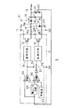
以下、本発明の電源装置の実施形態について図面を参照して説明する。図1に第1の実施形態の電源装置1の構成を示す。電源装置1は、入力端子11、出力端子12、スイッチ素子である2つのNMOSトランジスタ(以下、単にトランジスタと称す)13、14、コイル15、電解コンデンサ16、2つのツェナーダイオード(以下、単にダイオードと称す)17、18、2つのスイッチ19、20、および2つの抵抗21、22を備えている。
【0020】
入力端子11には変換の対象である電圧VINが与えられ、出力端子12には変換後の電圧VOUTを出力する。トランジスタ13は入力端子11とコイル15の一方の端子15aに接続されており、トランジスタ14の一端子は接地ライン23に接続されている。コイル15の他方の端子15bにはダイオード18のアノードが接続されており、ダイオード18のカソードは出力端子12に接続されている。ダイオード17のアノードは接地ライン23に接続されており、カソードはコイル15の端子15aに接続されている。コンデンサ16は出力端子12と接地ライン23に接続されている。抵抗21、22は直列に接続されており、出力端子12と接地ライン23とを接続している。
【0021】
スイッチ19は、コイル15の端子15bと出力端子12間に設けられており、閉結または開放の2状態をとる。スイッチ19の状態は端子S1を介して外部から与えられる制御信号によって切り換えられる。スイッチ19が閉結しているとき、コイル15と出力端子12は直接接続され、スイッチ19が開放しているとき、コイル15と出力端子12はダイオード18のみを介して接続される。
【0022】
スイッチ20は、トランジスタ14をコイル15の2つの端子15a、15bのどちらかに接続した2状態をとる。スイッチ20の状態は端子S2を介して外部から与えられる制御信号によって切り換えられる。スイッチ20がトランジスタ14を端子15aに接続させているとき、トランジスタ13とトランジスタ14は直接接続され、スイッチ20がトランジスタ14を端子15bに接続させているとき、トランジスタ13とトランジスタ14はコイル15を介して接続される。
【0023】
電源装置1は、また、トランジスタ13、14の動作を制御するために、2つの駆動回路31、32、発振器33、電圧シフト回路34、2つの比較器35、36、インバータ37、およびスイッチ38から成る制御部を備えている。駆動回路31、32は、それぞれトランジスタ13、14を駆動してそれらの導通と非導通の動作状態を切り換える。
【0024】
発振器33は、所定の最低値と所定の最高値間で変動する鋸歯状の電圧を、所定の短周期で発振して出力する。電圧シフト回路34は出力端子12に現れる電圧VOUTを抵抗21、22で分割した電圧を与えられる。電圧シフト回路34は2状態をとるスイッチ34aを備えており、スイッチ34aが一方の状態にあるときは、与えられた電圧を小さな所定値だけ低下させて出力し、スイッチ34aが他方の状態にあるときは与えられた電圧をそのまま出力する。スイッチ34aの状態は端子S3を介して外部から与えられる制御信号によって切り換えられる。
【0025】
比較器35は、出力端子12に現れる電圧VOUTを抵抗21、22で分割した電圧と発振器33の出力電圧を与えられて両者を比較し、前者が後者以上のときに出力する電圧をHレベルとし、前者が後者未満のときに出力する電圧をLレベルとする。比較器35の出力電圧は駆動回路31に与えられる。比較器36は、電圧シフト回路34の出力電圧と発振器33の出力電圧を与えられて両者を比較し、前者が後者以上のときに出力する電圧をHレベルとし、前者が後者未満のときに出力する電圧をLレベルとする。
【0026】
比較器36の出力電圧はインバータ37に与えられ、インバータ37は与えられた電圧のレベルを反転して出力する。スイッチ38は、比較器36の出力電圧を駆動回路32に与える状態と、インバータ37の出力電圧を駆動回路32に与える状態のいずれかをとる。スイッチ38の状態は端子S4を介して外部から与えられる制御信号によって切り換えられる。
【0027】
駆動回路31は、比較器35の出力電圧がHレベルのときにトランジスタ13を導通させず、Lレベルのときに導通させる。駆動回路32は、与えられる比較器36またはインバータ37の出力電圧が、Hレベルのときにトランジスタ14を導通させず、Lレベルのときに導通させる。比較器35、36は、トランジスタ13、14に与える駆動電圧をパルス幅変調(PWM)することになる。
【0028】
上記構成の電源装置1は、制御信号によって外部から与えられる指示に応じて2つの動作状態をとる。第1の状態においては、スイッチ19は閉結し、スイッチ20はコイル15の端子15aをトランジスタ14に接続し、電圧シフト回路34は分圧された出力電圧VOUTを低下させて出力し、スイッチ38はインバータ37の出力電圧を駆動回路32に与える。図1はこの状態に設定されている電源装置1を示している。
【0029】
この設定にあるとき、駆動回路31にLレベルが与えられている期間は、駆動回路32にはHレベルが与えられ、駆動回路31にHレベルが与えられている期間は、その最初と最後の一部を除き、駆動回路32にはLレベルが与えられることになる。駆動回路31にHレベルが与えられている期間の最初と最後には、駆動回路32にもHレベルが与えられる。したがって、トランジスタ13、14は発振器33の発振周波数によって定まる一定周期で略交互に導通し、しかも、同一時に導通することはない。
【0030】
トランジスタ13が導通しているとき、入力端子11から出力端子12に電流が流れ、同時にコイル15にエネルギーが蓄積される。トランジスタ13が導通を停止すると、コイル15に蓄積されたエネルギーにより逆起電力が生じ、ダイオード17を介して接地ライン23から電流が流れ込み、さらに、トランジスタ14が導通するとトランジスタ14を介して接地ライン23から電流が流れ込む。
【0031】
入力端子11から流れる電流と接地ライン23から流れ込む電流はコイル15およびコンデンサ16によって平滑化される。出力端子12に現れる電圧VOUTの高低に応じて、比較器35、36に与えられる分割電圧も変化する。この分割電圧が発振器33の出力電圧よりも高ければ比較器35の出力電圧がHレベルになる期間は増大し、低ければ減少する。同様に、分割電圧が電圧シフト回路34の出力電圧よりも高ければ比較器36の出力電圧がHレベルになる期間、すなわちインバータ37の出力電圧がLレベルになる期間は増大し、低ければ減少する。
【0032】
したがって、出力端子12の電圧VOUTが発振器33の発振電圧によって定まる所定値よりも高い期間が続くときには、トランジスタ13の導通時間を減少させて電圧VOUTを低下させるように動作し、出力端子12の電圧VOUTが所定値よりも低い期間が続くときには、トランジスタ13の導通時間を増大させて電圧VOUTを上昇させるように動作する。これにより、出力端子12に現れる電圧VOUTは略一定に保たれる。こうして、電源装置1は第1の状態にあるときは降圧用同期整流回路として機能する。
【0033】
第2の状態においては、スイッチ19は開放し、スイッチ20はコイル15の端子15bをトランジスタ14に接続し、電圧シフト回路34は与えられた電圧をそのまま出力し、スイッチ38は比較器36の出力電圧を駆動回路32に直接与える。この状態に設定されている電源装置1を図2に示す。
【0034】
この設定にあるとき、駆動回路31、32の入力には常に略同じタイミングで信号が与えられる。したがって、トランジスタ13、14は発振器33の発振周波数によって定まる一定周期で略同時に導通または遮断する。トランジスタ13、14が導通しているとき、入力端子11からコイル15を介して接地ライン23に電流が流れ、この間にコイル15にはエネルギーが蓄積される。このとき、ダイオード18には電流は流れず、コンデンサー16は充電されない。トランジスタ13、14が導通を停止すると、コイル15に蓄積されたエネルギーにより逆起電力が生じて、ダイオード17を介して接地ライン23から電流が流れ込む。流れ込んだ電流はダイオード18を通り、コンデンサー16が充電される。
【0035】
出力端子12に現れる電圧VOUTの高低に応じて、比較器35、36に与えられる分割電圧も変化する。この分割電圧が発振器33の出力電圧よりも高い期間が長ければ比較器35、36の出力電圧がHレベルになる期間は増大し、低い期間が長ければ減少する。したがって、出力端子12の電圧VOUTが発振器33の発振電圧によって定まる所定値よりも高い期間が長いときは、トランジスタ13、14の導通時間が減少して逆起電力も低下し、電圧VOUTは低下する。また、出力端子12の電圧VOUTが所定値よりも低い期間が長いときはトランジスタ13、14の導通時間が増大して逆起電力も増大し、電圧VOUTは上昇する。これにより、出力端子12に現れる電圧VOUTは略一定に保たれる。こうして、電源装置1は第2の状態にあるときは昇降圧用回路として機能する。
【0036】
なお、制御部の全てとトランジスタ13、14は1つのチップCに集積回路として形成されており、コイル15やコンデンサ16をはじめとする他の構成要素は、チップCに対して外付けされている。
【0037】
上記の電源装置1の制御部をより具体化した第2の実施形態の電源装置2について説明する。電源装置2の構成を図3に示す。入力端子から出力端子に至る構成は電源装置1と同じである。以下、電源装置1と同じ構成要素には同じ符号を付して、説明を省略する。電源装置2は制御部として、発振器33、比較器35、36のほか、駆動回路41、42、電圧シフト回路44、EXNOR回路45、エラーアンプ46およびコンデンサ47を備えている。
【0038】
駆動回路41、42はそれぞれインバータを4段接続して成り、与えられる電圧を段階的に増幅してトランジスタ13、14を駆動する。エラーアンプ46とコンデンサ47は、出力端子12の電圧VOUTを分割した電圧の微小な変動を除去し、変動除去後の電圧を増幅して出力する。
【0039】
電圧シフト回路44は、スイッチ44a、定電圧源44b、オペアンプ44c、44d、PNP型のトランジスタ44e、および抵抗44f、44gより成る。オペアンプ44cはエラーアンプ46の出力電圧をそのまま出力し、抵抗44fを介して比較器36に与える。スイッチ44aは端子S3を介して外部から与えられる制御信号に応じてオペアンプ44dを定電圧源44bまたは接地ラインに接続する。
【0040】
定電圧源44bに接続されているときオペアンプ44dは動作してトランジスタ44eを導通させる。これにより抵抗44gにも電流が流れて、オペアンプ44cから抵抗44fを介して比較器36に与えられる電圧は低下する。接地ラインに接続されているときオペアンプ44dは動作せず、トランジスタ44eは導通しない。このとき比較器36にはオペアンプ44cの出力電圧がそのまま与えられる。こうして電圧シフト回路は44、エラーアンプ46の出力電圧を低下させる状態とさせない状態とをとる。
【0041】
EXNOR回路45は、比較器36の出力電圧と端子S4を介して外部から与えられる制御信号のレベルの排他的論理和を求め、その否定結果を出力する。制御信号がLレベルのときEXNOR回路45の出力電圧は、比較器36の出力電圧がHレベルであればLレベルとなり、比較器36の出力電圧がLレベルであればHレベルとなる。このとき、EXNOR回路45はインバータとして機能する。
【0042】
また、制御信号がHレベルのときEXNOR回路45の出力電圧は、比較器36の出力電圧がHレベルであればHレベルとなり、比較器36の出力電圧がLレベルであればLレベルとなる。このとき、EXNOR回路45は入力電圧をそのまま出力することになる。したがって、EXNOR回路45は、電源装置1のインバータ37とスイッチ38の両方の機能を兼ねる。
【0043】
電源装置2も、外部から与えられる指示に応じて2つの動作状態をとる。第1の状態においては、スイッチ19は閉結し、スイッチ20はコイル15の端子15aをトランジスタ14に接続し、スイッチ44aはオペアンプ44dを定電圧源44bに接続する。また、EXNOR回路45に与えられる制御信号はLレベルである。図3はこの状態に設定されている電源装置2を示しており、このとき、電源装置2は降圧用同期整流回路として機能する。
【0044】
第2の状態においては、スイッチ19は開放し、スイッチ20はコイル15の端子15bをトランジスタ14に接続し、スイッチ44aはオペアンプ44dを接地ラインに接続する。また、EXNOR回路45に与えられる制御信号はHレベルである。この状態に設定されている電源装置2を図4に示す。このとき、電源装置2は昇降圧用回路として機能する。
【0045】
第3の実施形態の電源装置3の構成を図5に示す。この電源装置3は、第1の実施形態の電源装置1のスイッチ38に代えてスイッチ39を備え、電圧シフト回路34からスイッチ34aを省略したものである。インバータ37は比較器36に直接接続されている。スイッチ39は、降圧用同期整流回路として動作する第1の状態においては、インバータ37を駆動回路32に接続し、昇降圧用回路として動作する第2の状態においては、比較器35を駆動回路32に接続する。
【0046】
電源装置3は、電源装置1と比較して、動作状態の切り換えのために必要なスイッチが少なくなっており、構成が簡単になっている。当然、電源装置3に与える制御信号の数も少なくなり、動作状態の切り換え制御も容易になる。なお、端子S4を介してスイッチ39に与えられる制御信号を電圧シフト回路34にも与え、スイッチ39が比較器35と駆動回路32を接続している間に電圧シフト回路34の動作を停止させるようにしてもよい。そのようにすると、昇降圧用回路として動作する期間に電力消費を低減することができて好ましい。
【0047】
【発明の効果】
本発明の電源装置は、降圧用同期整流回路の機能と昇降圧用回路の機能を併せもちながらも、ほとんど全ての構成要素を両機能に兼用するから、構成に無駄がない。したがって、コストが低下し、装置も小型となる。
【図面の簡単な説明】
【図1】 第1の実施形態の電源装置の構成および降圧用同期整流回路として動作するときの設定を示す図。
【図2】 第1の実施形態の電源装置の構成および昇降圧用回路として動作するときの設定を示す図。
【図3】 第2の実施形態の電源装置の構成および降圧用同期整流回路として動作するときの設定を示す図。
【図4】 第2の実施形態の電源装置の構成および昇降圧用回路として動作するときの設定を示す図。
【図5】 第3の実施形態の電源装置の構成および降圧用同期整流回路として動作するときの設定を示す図。
【図6】 従来の降圧用同期整流回路の構成を示す図。
【図7】 従来の昇降圧用回路の構成を示す図。
【符号の説明】
1、2、3 電源装置
11 入力端子
12 出力端子
13、14 トランジスタ
15 コイル
16 コンデンサ
17、18 ダイオード
19 スイッチ
20 スイッチ
21、22 抵抗
31、32 駆動回路
33 発振器
34 電圧シフト回路
34a スイッチ
35、36 比較器
37 インバータ
38 スイッチ
39 スイッチ
41、42 駆動回路
44 電圧シフト回路
44a スイッチ
44c、44d オペアンプ
44e トランジスタ
45 EXNOR回路
46 エラーアンプ
47 コンデンサ
S1、S2、S3、S4 制御端子[0001]
BACKGROUND OF THE INVENTION
The present invention relates to a power supply device that converts an input voltage into a predetermined voltage by a chopper method and outputs the voltage, and more particularly relates to a power supply device that has the functions of a step-down synchronous rectifier circuit and a step-up / step-down circuit.
[0002]
[Prior art]
A chopper-type synchronous rectification circuit that efficiently lowers an input voltage higher than a predetermined voltage to a predetermined voltage, an input voltage lower than the predetermined voltage is increased to a predetermined voltage, and an input voltage higher than the predetermined voltage is decreased to the predetermined voltage There is also a chopper-type step-up / down circuit. The configurations of a conventional step-down synchronous rectifier circuit and a step-up / step-down circuit are shown in FIGS. 6 and 7, respectively.
[0003]
6 includes a
[0004]
In order to control the
[0005]
The
[0006]
By this control, the
[0007]
The current flowing from the
[0008]
7 includes a
[0009]
An
[0010]
By this control, the
[0011]
Depending on the level of the voltage appearing at the
[0012]
The step-down synchronous rectifier circuit allows a current to flow from an input terminal to an output terminal, and also allows a current to flow from a ground line through a transistor as well as a diode, so that the voltage conversion efficiency is extremely high. On the other hand, the predetermined voltage can be output only when the input voltage is equal to or higher than the predetermined voltage determined as the output voltage. On the other hand, the step-up / step-down circuit does not flow current from the input terminal to the output terminal, and uses the current only for generating the counter electromotive force, so that the conversion efficiency is not so good. On the other hand, even if the input voltage is equal to or higher than the predetermined voltage determined as the output voltage or less than the predetermined voltage, the predetermined voltage can be output.
[0013]
[Problems to be solved by the invention]
If the supplied voltage is higher than the required predetermined voltage, it is advantageous to use a step-down synchronous rectifier circuit. However, the supplied voltage is not always higher than the required predetermined voltage. In such a case, either a step-down / step-down circuit with inferior efficiency is used, or both circuits are provided, depending on the supplied voltage. The efficiency is improved by obtaining a predetermined voltage in the circuit. For this reason, a power supply apparatus including a step-down synchronous rectifier circuit and a step-up / step-down circuit is also used.
[0014]
As apparent from comparison between FIG. 6 and FIG. 7, the configurations of the step-down synchronous rectifier circuit and the step-up / step-down circuit are similar. However, conventionally, since the step-down synchronous rectifier circuit and the step-up / step-down circuit are simply arranged side by side, there are two components that control the same function, and the configuration is wasteful.
[0015]
The present invention has been made in view of the above-described problems, and an object of the present invention is to provide a power supply device that has both the function of a step-down synchronous rectifier circuit and the function of a step-up / step-down circuit and has no wasteful structure.
[0016]
[Means for Solving the Problems]
In order to achieve the above object, in the present invention, a voltage applied to an input terminal is converted into a predetermined voltage by a chopper method and output from the output terminal, a ground line connected to the ground potential, a coil, one end Is connected to the output terminal and the other end is connected to the ground line, one end is connected to the input terminal, and the other end is connected to the first terminal of the coil. A first diode having an anode connected to the ground line and a cathode connected to the first terminal of the coil; a second switch element having one end connected to the ground line and a conductive state and a non-conductive state; the anode being a coil A second diode having a cathode connected to the output terminal and a second terminal of the coil connected to the output terminal or via a second diode. First switching means for switching whether to continue, second switching means for exclusively connecting the first terminal and the second terminal of the coil to the other end of the second switching element, and the first switching element and A control unit is provided that intermittently conducts the second switch element at a predetermined short period.
[0017]
When the first switching means connects the second terminal and the output terminal of the coil, and the second switching means connects the first terminal of the coil to the second switch element, the control unit causes the first switching means to By switching the switch element and the second switch element substantially alternately, the applied voltage is lowered to a predetermined voltage and output. Thus, the function of the step-down synchronous rectifier circuit is realized, and when the voltage applied to the input terminal is higher than the predetermined voltage, the voltage can be efficiently converted into the predetermined voltage.
[0018]
The second switching means connects the second diode between the second terminal and the output terminal of the coil, and the second switching means connects the second terminal of the coil to the second switch element. In some cases, the control unit causes the first switch element and the second switch element to conduct substantially simultaneously, thereby increasing or decreasing the applied voltage to a predetermined voltage and outputting the voltage. Thereby, the function of the step-up / step-down circuit is realized, and the voltage applied to the input terminal can be converted into a predetermined voltage regardless of whether it is higher or lower than the predetermined voltage.
[0019]
DETAILED DESCRIPTION OF THE INVENTION
Hereinafter, embodiments of a power supply device of the present invention will be described with reference to the drawings. FIG. 1 shows a configuration of a
[0020]
The
[0021]
The
[0022]
The
[0023]
The
[0024]
The
[0025]
The
[0026]
The output voltage of the
[0027]
The
[0028]
The
[0029]
In this setting, during the period in which the
[0030]
When the
[0031]
The current flowing from the
[0032]
Accordingly, when the period during which the voltage VOUT at the
[0033]
In the second state, the
[0034]
In this setting, signals are always given to the inputs of the
[0035]
The divided voltage applied to the
[0036]
All the control units and the
[0037]
A
[0038]
Each of the
[0039]
The
[0040]
When connected to the
[0041]
The
[0042]
When the control signal is at the H level, the output voltage of the
[0043]
The
[0044]
In the second state, the
[0045]
The configuration of the
[0046]
Compared with the
[0047]
【The invention's effect】
The power supply apparatus according to the present invention has the function of the step-down synchronous rectifier circuit and the function of the step-up / step-down circuit, but uses almost all the constituent elements for both functions. Therefore, the cost is reduced and the apparatus is also downsized.
[Brief description of the drawings]
FIG. 1 is a diagram showing a configuration of a power supply device according to a first embodiment and settings when operating as a step-down synchronous rectifier circuit.
FIG. 2 is a diagram showing a configuration of the power supply device according to the first embodiment and settings when operating as a step-up / down circuit.
FIG. 3 is a diagram showing a configuration of a power supply device according to a second embodiment and settings when operating as a step-down synchronous rectifier circuit.
FIG. 4 is a diagram showing a configuration of a power supply device according to a second embodiment and settings when operating as a step-up / down circuit.
FIG. 5 is a diagram showing a configuration of a power supply device according to a third embodiment and settings when operating as a step-down synchronous rectifier circuit.
FIG. 6 is a diagram showing a configuration of a conventional step-down synchronous rectifier circuit.
FIG. 7 is a diagram showing a configuration of a conventional step-up / step-down circuit.
[Explanation of symbols]
1, 2, 3
Claims (1)
グランド電位に接続された接地ライン、
コイル、
一端が前記出力端子に接続され他端が前記接地ラインに接続されたコンデンサ、
一端が前記入力端子に接続され他端が前記コイルの第1の端子に接続された導通状態と非導通状態をとる第1のスイッチ素子、
アノードが前記接地ラインに接続されカソードが前記コイルの第1の端子に接続された第1のダイオード、
一端が前記接地ラインに接続された導通状態と非導通状態をとる第2のスイッチ素子、
アノードが前記コイルの第2の端子に接続されカソードが前記出力端子に接続された第2のダイオード、
前記コイルの第2の端子と前記出力端子とを短絡接続するか前記第2のダイオードを介して接続するかを切り換える第1の切り換え手段、
前記コイルの第1の端子と第2の端子を排他的に前記第2のスイッチ素子の他端に接続する第2の切り換え手段、ならびに
前記第1のスイッチ素子および前記第2のスイッチ素子を所定の短周期でそれぞれ断続的に導通させる制御部を備え、
前記第1の切り換え手段により前記コイルの第2の端子と前記出力端子を接続し、前記第2の切り換え手段により前記コイルの第1の端子を前記第2のスイッチ素子に接続するときには、前記制御部により前記第1のスイッチ素子と前記第2のスイッチ素子を略交互に導通させることにより、与えられる電圧を所定の電圧まで下降させて出力し、
前記第1の切り換え手段により前記コイルの第2の端子と前記出力端子との間に前記第2のダイオードを接続し、前記第2の切り換え手段により前記コイルの第2の端子を前記第2のスイッチ素子に接続するときには、前記制御部により前記第1のスイッチ素子と前記第2のスイッチ素子を略同時に導通させることにより、与えられる電圧を所定の電圧まで上昇または下降させて出力する
ことを特徴とする電源装置。In the power supply device that converts the voltage given to the input terminal to a predetermined voltage by the chopper method and outputs it from the output terminal,
A ground line connected to the ground potential,
coil,
A capacitor having one end connected to the output terminal and the other end connected to the ground line;
A first switching element that has a conductive state and a non-conductive state in which one end is connected to the input terminal and the other end is connected to the first terminal of the coil;
A first diode having an anode connected to the ground line and a cathode connected to a first terminal of the coil;
A second switch element having one end connected to the ground line and taking a conductive state and a non-conductive state;
A second diode having an anode connected to the second terminal of the coil and a cathode connected to the output terminal;
A first switching means for switching whether the second terminal of the coil and the output terminal are short-circuited or connected via the second diode;
A second switching means for exclusively connecting the first terminal and the second terminal of the coil to the other end of the second switch element; and the first switch element and the second switch element A control unit that intermittently conducts in a short period of time,
When the first switching means connects the second terminal of the coil and the output terminal, and the second switching means connects the first terminal of the coil to the second switch element, the control The first switch element and the second switch element are made to conduct substantially alternately by the unit, and the applied voltage is lowered to a predetermined voltage and output,
The second switching means connects the second diode between the second terminal and the output terminal of the coil, and the second switching means connects the second terminal of the coil to the second terminal. When connecting to a switch element, the control unit causes the first switch element and the second switch element to conduct substantially simultaneously, thereby increasing or decreasing a given voltage to a predetermined voltage and outputting the voltage. Power supply.
Priority Applications (1)
| Application Number | Priority Date | Filing Date | Title |
|---|---|---|---|
| JP26418298A JP3963590B2 (en) | 1998-09-18 | 1998-09-18 | Power supply |
Applications Claiming Priority (1)
| Application Number | Priority Date | Filing Date | Title |
|---|---|---|---|
| JP26418298A JP3963590B2 (en) | 1998-09-18 | 1998-09-18 | Power supply |
Publications (2)
| Publication Number | Publication Date |
|---|---|
| JP2000092825A JP2000092825A (en) | 2000-03-31 |
| JP3963590B2 true JP3963590B2 (en) | 2007-08-22 |
Family
ID=17399616
Family Applications (1)
| Application Number | Title | Priority Date | Filing Date |
|---|---|---|---|
| JP26418298A Expired - Fee Related JP3963590B2 (en) | 1998-09-18 | 1998-09-18 | Power supply |
Country Status (1)
| Country | Link |
|---|---|
| JP (1) | JP3963590B2 (en) |
Families Citing this family (3)
| Publication number | Priority date | Publication date | Assignee | Title |
|---|---|---|---|---|
| JP4850344B2 (en) * | 2001-03-05 | 2012-01-11 | 富士通セミコンダクター株式会社 | DC-DC converter control circuit and DC-DC converter |
| JP3784745B2 (en) * | 2002-04-22 | 2006-06-14 | 株式会社ジェイテクト | Motor control device |
| JP2006271182A (en) * | 2005-02-25 | 2006-10-05 | Rohm Co Ltd | Voltage regulator circuit and liquid crystal display using the same |
-
1998
- 1998-09-18 JP JP26418298A patent/JP3963590B2/en not_active Expired - Fee Related
Also Published As
| Publication number | Publication date |
|---|---|
| JP2000092825A (en) | 2000-03-31 |
Similar Documents
| Publication | Publication Date | Title |
|---|---|---|
| KR100702721B1 (en) | A dc/dc up/down converter | |
| JP3175227B2 (en) | DC / DC voltage converter | |
| US7486055B2 (en) | DC-DC converter having a diode module with a first series circuit and a second series with a flywheel diode | |
| US20060170400A1 (en) | Dual-input power converter and control methods thereof | |
| JP4636249B2 (en) | Current resonance type DC / DC converter and method for realizing zero current switching thereof | |
| US20070216387A1 (en) | Switching regulator and method for changing output voltages thereof | |
| KR20090132497A (en) | Dc-dc converter | |
| JP2004173460A (en) | Dc-dc converter control method, dc-dc converter, semiconductor integrated circuit, and electronic apparatus | |
| JPH06311736A (en) | Dc/dc converter | |
| JPH0556636A (en) | Voltage converter | |
| JP2007028829A (en) | Current resonance dc-dc converter and its resonance current control method | |
| JP2009112142A (en) | Converter circuit and control method of converter | |
| CN113708626A (en) | Hundred percent duty cycle generating circuit suitable for COT voltage converter | |
| JP3963590B2 (en) | Power supply | |
| JP2002078325A (en) | Dc-dc converter and electronic apparatus using the same | |
| EP1478084B1 (en) | A digital power converting method and device with zero voltage | |
| JP2001112241A (en) | Synchronous-rectification type dc/dc converter | |
| CN113783421A (en) | Direct current conversion equipment that steps up | |
| JP2003164142A (en) | Voltage conversion circuit | |
| JP3003437B2 (en) | Voltage converter | |
| JP3699011B2 (en) | Switching regulator | |
| JPH0766700A (en) | Controller for power mosfet | |
| JP2003257692A (en) | Discharge lamp lighting circuit | |
| JPH10323027A (en) | Power supply circuit | |
| JPH08107669A (en) | Step-up chopper regulator |
Legal Events
| Date | Code | Title | Description |
|---|---|---|---|
| A621 | Written request for application examination |
Free format text: JAPANESE INTERMEDIATE CODE: A621 Effective date: 20041126 |
|
| TRDD | Decision of grant or rejection written | ||
| A01 | Written decision to grant a patent or to grant a registration (utility model) |
Free format text: JAPANESE INTERMEDIATE CODE: A01 Effective date: 20070522 |
|
| A61 | First payment of annual fees (during grant procedure) |
Free format text: JAPANESE INTERMEDIATE CODE: A61 Effective date: 20070522 |
|
| R150 | Certificate of patent or registration of utility model |
Free format text: JAPANESE INTERMEDIATE CODE: R150 |
|
| FPAY | Renewal fee payment (event date is renewal date of database) |
Free format text: PAYMENT UNTIL: 20100601 Year of fee payment: 3 |
|
| FPAY | Renewal fee payment (event date is renewal date of database) |
Free format text: PAYMENT UNTIL: 20110601 Year of fee payment: 4 |
|
| FPAY | Renewal fee payment (event date is renewal date of database) |
Free format text: PAYMENT UNTIL: 20120601 Year of fee payment: 5 |
|
| FPAY | Renewal fee payment (event date is renewal date of database) |
Free format text: PAYMENT UNTIL: 20120601 Year of fee payment: 5 |
|
| FPAY | Renewal fee payment (event date is renewal date of database) |
Free format text: PAYMENT UNTIL: 20130601 Year of fee payment: 6 |
|
| LAPS | Cancellation because of no payment of annual fees |