EP1077466A2 - Flat-panel display with controlled sustaining electrodes - Google Patents
Flat-panel display with controlled sustaining electrodes Download PDFInfo
- Publication number
- EP1077466A2 EP1077466A2 EP00117638A EP00117638A EP1077466A2 EP 1077466 A2 EP1077466 A2 EP 1077466A2 EP 00117638 A EP00117638 A EP 00117638A EP 00117638 A EP00117638 A EP 00117638A EP 1077466 A2 EP1077466 A2 EP 1077466A2
- Authority
- EP
- European Patent Office
- Prior art keywords
- electrodes
- voltage
- sustaining
- auxiliary
- substrate
- Prior art date
- Legal status (The legal status is an assumption and is not a legal conclusion. Google has not performed a legal analysis and makes no representation as to the accuracy of the status listed.)
- Withdrawn
Links
Images




Classifications
-
- H—ELECTRICITY
- H01—ELECTRIC ELEMENTS
- H01J—ELECTRIC DISCHARGE TUBES OR DISCHARGE LAMPS
- H01J11/00—Gas-filled discharge tubes with alternating current induction of the discharge, e.g. alternating current plasma display panels [AC-PDP]; Gas-filled discharge tubes without any main electrode inside the vessel; Gas-filled discharge tubes with at least one main electrode outside the vessel
- H01J11/20—Constructional details
- H01J11/22—Electrodes, e.g. special shape, material or configuration
- H01J11/24—Sustain electrodes or scan electrodes
-
- H—ELECTRICITY
- H01—ELECTRIC ELEMENTS
- H01J—ELECTRIC DISCHARGE TUBES OR DISCHARGE LAMPS
- H01J11/00—Gas-filled discharge tubes with alternating current induction of the discharge, e.g. alternating current plasma display panels [AC-PDP]; Gas-filled discharge tubes without any main electrode inside the vessel; Gas-filled discharge tubes with at least one main electrode outside the vessel
- H01J11/20—Constructional details
- H01J11/22—Electrodes, e.g. special shape, material or configuration
- H01J11/28—Auxiliary electrodes, e.g. priming electrodes or trigger electrodes
-
- G—PHYSICS
- G09—EDUCATION; CRYPTOGRAPHY; DISPLAY; ADVERTISING; SEALS
- G09G—ARRANGEMENTS OR CIRCUITS FOR CONTROL OF INDICATING DEVICES USING STATIC MEANS TO PRESENT VARIABLE INFORMATION
- G09G3/00—Control arrangements or circuits, of interest only in connection with visual indicators other than cathode-ray tubes
- G09G3/20—Control arrangements or circuits, of interest only in connection with visual indicators other than cathode-ray tubes for presentation of an assembly of a number of characters, e.g. a page, by composing the assembly by combination of individual elements arranged in a matrix no fixed position being assigned to or needed to be assigned to the individual characters or partial characters
- G09G3/22—Control arrangements or circuits, of interest only in connection with visual indicators other than cathode-ray tubes for presentation of an assembly of a number of characters, e.g. a page, by composing the assembly by combination of individual elements arranged in a matrix no fixed position being assigned to or needed to be assigned to the individual characters or partial characters using controlled light sources
- G09G3/28—Control arrangements or circuits, of interest only in connection with visual indicators other than cathode-ray tubes for presentation of an assembly of a number of characters, e.g. a page, by composing the assembly by combination of individual elements arranged in a matrix no fixed position being assigned to or needed to be assigned to the individual characters or partial characters using controlled light sources using luminous gas-discharge panels, e.g. plasma panels
- G09G3/288—Control arrangements or circuits, of interest only in connection with visual indicators other than cathode-ray tubes for presentation of an assembly of a number of characters, e.g. a page, by composing the assembly by combination of individual elements arranged in a matrix no fixed position being assigned to or needed to be assigned to the individual characters or partial characters using controlled light sources using luminous gas-discharge panels, e.g. plasma panels using AC panels
- G09G3/298—Control arrangements or circuits, of interest only in connection with visual indicators other than cathode-ray tubes for presentation of an assembly of a number of characters, e.g. a page, by composing the assembly by combination of individual elements arranged in a matrix no fixed position being assigned to or needed to be assigned to the individual characters or partial characters using controlled light sources using luminous gas-discharge panels, e.g. plasma panels using AC panels using surface discharge panels
- G09G3/2983—Control arrangements or circuits, of interest only in connection with visual indicators other than cathode-ray tubes for presentation of an assembly of a number of characters, e.g. a page, by composing the assembly by combination of individual elements arranged in a matrix no fixed position being assigned to or needed to be assigned to the individual characters or partial characters using controlled light sources using luminous gas-discharge panels, e.g. plasma panels using AC panels using surface discharge panels using non-standard pixel electrode arrangements
- G09G3/2986—Control arrangements or circuits, of interest only in connection with visual indicators other than cathode-ray tubes for presentation of an assembly of a number of characters, e.g. a page, by composing the assembly by combination of individual elements arranged in a matrix no fixed position being assigned to or needed to be assigned to the individual characters or partial characters using controlled light sources using luminous gas-discharge panels, e.g. plasma panels using AC panels using surface discharge panels using non-standard pixel electrode arrangements with more than 3 electrodes involved in the operation
-
- H—ELECTRICITY
- H01—ELECTRIC ELEMENTS
- H01J—ELECTRIC DISCHARGE TUBES OR DISCHARGE LAMPS
- H01J11/00—Gas-filled discharge tubes with alternating current induction of the discharge, e.g. alternating current plasma display panels [AC-PDP]; Gas-filled discharge tubes without any main electrode inside the vessel; Gas-filled discharge tubes with at least one main electrode outside the vessel
- H01J11/10—AC-PDPs with at least one main electrode being out of contact with the plasma
- H01J11/12—AC-PDPs with at least one main electrode being out of contact with the plasma with main electrodes provided on both sides of the discharge space
-
- H—ELECTRICITY
- H01—ELECTRIC ELEMENTS
- H01J—ELECTRIC DISCHARGE TUBES OR DISCHARGE LAMPS
- H01J11/00—Gas-filled discharge tubes with alternating current induction of the discharge, e.g. alternating current plasma display panels [AC-PDP]; Gas-filled discharge tubes without any main electrode inside the vessel; Gas-filled discharge tubes with at least one main electrode outside the vessel
- H01J11/20—Constructional details
- H01J11/34—Vessels, containers or parts thereof, e.g. substrates
- H01J11/38—Dielectric or insulating layers
-
- H—ELECTRICITY
- H01—ELECTRIC ELEMENTS
- H01J—ELECTRIC DISCHARGE TUBES OR DISCHARGE LAMPS
- H01J11/00—Gas-filled discharge tubes with alternating current induction of the discharge, e.g. alternating current plasma display panels [AC-PDP]; Gas-filled discharge tubes without any main electrode inside the vessel; Gas-filled discharge tubes with at least one main electrode outside the vessel
- H01J11/20—Constructional details
- H01J11/34—Vessels, containers or parts thereof, e.g. substrates
- H01J11/42—Fluorescent layers
-
- G—PHYSICS
- G09—EDUCATION; CRYPTOGRAPHY; DISPLAY; ADVERTISING; SEALS
- G09G—ARRANGEMENTS OR CIRCUITS FOR CONTROL OF INDICATING DEVICES USING STATIC MEANS TO PRESENT VARIABLE INFORMATION
- G09G2320/00—Control of display operating conditions
- G09G2320/02—Improving the quality of display appearance
- G09G2320/0228—Increasing the driving margin in plasma displays
-
- H—ELECTRICITY
- H01—ELECTRIC ELEMENTS
- H01J—ELECTRIC DISCHARGE TUBES OR DISCHARGE LAMPS
- H01J2211/00—Plasma display panels with alternate current induction of the discharge, e.g. AC-PDPs
- H01J2211/20—Constructional details
- H01J2211/22—Electrodes
- H01J2211/32—Disposition of the electrodes
- H01J2211/323—Mutual disposition of electrodes
Definitions
- This invention relates in general to a flat-panel display and in particular to an improved structure for a full color, high resolution capable flat-panel display which operates at a high efficiency.
- the basic structure of an AC Plasma Display Panel, or PDP comprises two glass plates with a conductor pattern of electrodes on the inner surfaces of each plate.
- the plates are separated by a gas filled gap.
- the electrodes are configured in an x-y matrix with the electrodes on each plate deposited at right angles to each other using conventional thin of thick film techniques.
- At least one set of sustaining electrodes of the AC PDP is covered with a thin glass dielectric layer.
- the glass plates are assembled into a sandwich with the gap between the plates fixed by spacers. The edges of the plates are sealed and the cavity between the plates is evacuated and filled with a mixture of neon and xenon gases or a similar gas mixture of a type well known in the art.
- a sufficient driver voltage pulse is applied to the electrodes to ionize the gas contained between the plates.
- the dielectrics charge like small capacitors, which reduces the voltage across the gas and extinguishes the discharge.
- the capacitive voltages are due to stored charge and are conventionally called wall charge.
- the voltage is then reversed, and the sum of the driver voltage and wall charge voltages is again large enough to excite the gas and produce a glow discharge pulse.
- a sequence of such driver voltages repetitively applied is called the sustaining voltage, or sustainer.
- sustainer waveform pixels which have had charge stored will discharge and emit light pulses at every sustainer cycle. Pixels which have no charge stored will not emit light.
- appropriate waveforms are applied across the x-y matrix of electrodes, small light emitting pixels form a visual picture.
- barrier ribs are typically disposed between the plates to prevent cross-color and cross-pixel interference between the electrodes.
- the barrier ribs also increase the resolution to provide a sharply defined picture.
- the barrier ribs further provide a uniform discharge space between the glass plates by utilizing the barrier rib height, width and pattern gap to achieve a desired pixel pitch.
- This invention relates to an improved plasma flat-panel display which includes at least one auxiliary electrode disposed between each pair of sustaining electrodes.
- plasma flat-panel displays having pairs of sustaining electrodes which establish a charged volume between the display substrates.
- the charge is controlled by applying voltages to a plurality of address electrodes.
- the charged volume is established by applying a voltage to the sustaining electrodes.
- the efficiency of the panel is generally greater when gas and geometry parameters are adjusted to increase the voltage required to sustain a discharge.
- this is in conflict with the need to have low voltages for economic and reliability purposes. Therefore, it would be desirable to develop a compromise device which would allow initiation and control of the sustaining discharge with a less powerful and lower voltage controlling means.
- the present invention contemplates a plasma flat-panel display having a first transparent substrate with at least one pair of parallel sustaining electrodes deposited thereupon. A least one auxiliary electrode is deposited upon the first substrate parallel to the sustaining electrodes.
- the panel also includes an charge storage surface coating which covers the sustaining and auxiliary electrode.
- the panel further includes a second substrate which is hermetically sealed to the first substrate, the second substrate, having a plurality of gas-filled micro-voids formed in a surface thereof which is adjacent to the first substrate.
- the micro-voids are generally perpendicular to the sustaining and auxiliary electrodes and cooperate with the first substrate to define a plurality of sub-pixels.
- a plurality of address electrodes are incorporated within the second substrate, each of the address electrodes corresponding to one of the sub-pixels.
- a first voltage is applied to the auxiliary electrode of sufficient magnitude to inject a charge of electrons between the auxiliary electrode and an associated sustaining electrode and initiate a discharge therebetween.
- a second voltage that is greater than the first voltage is applied to the sustaining electrodes to extend the discharge to the other sustaining electrode.
- the voltage applied to the auxiliary electrode can be changed to urge the discharge deeper into the associated micro-void.
- the first voltage is applied before the second voltage; however, the invention also can be practiced with the first and second voltages being applied simultaneously or with the second voltage applied before the first voltage.
- the discharge between the sustaining electrodes can be controlled by applying a third voltage to the address electrodes.
- a phosphor material is deposited within each micro-void and associated with the address electrodes.
- the first and second substrates are formed from glass.
- the invention can be practiced having a pair of auxiliary electrodes disposed between the sustaining electrodes.
- the channels 32 are filled with a proportioned mixture of two or more ionizable gases which produces sufficient UV radiation to excite the phosphor material 38.
- a gas mixture of neon and from about five to 20 percent by weight of xenon and helium is used.
- a discharge is initiated between a selected pair of auxiliary electrodes 24 by applying a first voltage across the auxiliary electrodes. Because the auxiliary electrodes are relatively dose together, the first voltage needed to initiate the discharge is less than the voltage required to initiate a discharge between the sustaining electrodes.
- the second auxiliary electrode 66 is separated from the right sustaining electrode 64 by about 40 microns to 100 microns.
- the second set of electrodes 62 includes a pair of sustaining electrodes 67 having first and second auxiliary electrodes 68 and 69 disposed adjacent thereto.
- a first voltage is applied to the first auxiliary electrode 65 which establishes a starting charge of electrons between the first auxiliary electrode 65 and the left sustaining electrode 63.
- the charge of electrons may be the result of a relatively small discharge between the auxiliary electrode 65 and a sustaining electrode 63.
- the starting charge enables establishment of a relatively larger discharge between the sustaining electrodes 63 and 64 with a lower sustaining voltage than would be needed in the absence of the starting charge.
- the sustaining electrode 63 be a cathode with respect to the auxiliary electrode 65 at this phase of the operation.
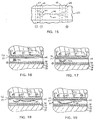
- FIG. 16 An alternate three-step method for initiating a discharge is illustrated in Figs. 16 through 19.
- a first voltage is applied between the left sustaining electrode 63 and the opposite address electrode 36.
- the left sustaining electrode 63 is negative relative to the address electrode 36 and functions as a cathode.
- An initial discharge 106 is established in Fig. 16 between the left sustaining electrode 63 and the address electrode 36.
- the initial discharge 106 is moved to the right in Fig. 17 by application of a second voltage between the left sustaining electrode 63 and the first auxiliary electrode 65 to establish the cathode fall region 102 described above.
- the operation then proceeds as described above with a third sustaining voltage applied between the sustaining electrodes 63 and 64 in Fig. 18.
Landscapes
- Engineering & Computer Science (AREA)
- Physics & Mathematics (AREA)
- Plasma & Fusion (AREA)
- Chemical & Material Sciences (AREA)
- Materials Engineering (AREA)
- Power Engineering (AREA)
- Computer Hardware Design (AREA)
- General Physics & Mathematics (AREA)
- Theoretical Computer Science (AREA)
- Gas-Filled Discharge Tubes (AREA)
- Control Of Indicators Other Than Cathode Ray Tubes (AREA)
- Control Of Gas Discharge Display Tubes (AREA)
Abstract
Description
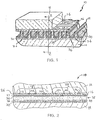
- Fig. 1
- is a perspective view of a plasma display panel in accordance with the invention.
- Fig. 2
- is sectional view of the plasma display panel in Fig. 1 taken along line 2-2.
- Fig. 3
- illustrates the operation of the plasma display panel shown in Fig. 1.
- Fig. 4
- also illustrates the operation of the plasma display panel shown in Fig. 1.
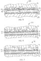
- Fig. 5
- is a sectional view of an alternate embodiment of the plasma display panel shown in Fig. 1.
- Fig. 6
- is a sectional view of another alternate embodiment of the plasma display panel shown in Fig. 1 .
- Fig. 7
- is a sectional view of another alternate embodiment of the plasma display panel shown in Fig. 1 .
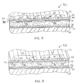
- Fig. 8
- is a sectional view of an alternate embodiment of the plasma display panel shown in Fig. 6.
- Fig. 9
- is a sectional view of an alternate embodiment of the plasma display panel shown in Fig. 8.
- Fig. 10
- illustrates a first step; of an alternate method for operating the plasma display panel shown in Fig. 6 which is in accordance with the invention.
- Fig. 11
- illustrates a second step in the method of operation shown in Fig. 10.
- Fig. 12
- is a transverse view of the plasma display panel shown taken along line 12-12 in Fig. 11.
- Fig. 13
- illustrates a third step in the method of operation shown in Fig. 10.
- Fig. 14
- is a transverse view of the plasma display panel shown taken along line 14-14 in Fig. 13.
- Fig. 15
- is a plan view of the plasma display panel taken along line 15-15 in Fig. 13.
- Fig. 16
- is a first step of an alternate embodiment of the method of operation of the plasma display panel shown in Figs. 10 through 15.
- Fig. 17
- is a second step in the method shown in Fig. 16.
- Fig. 18
- is a third step in the method shown in Fig. 16.
- Fig. 19
- is a fourth step in the method shown in Fig. 16.
- Fig. 20
- is a first step of an alternate embodiment of the method of operation of the plasma display panel shown in Figs. 10 through 15.
- Fig. 21
- is second step in the method shown in Fig. 20.
- Fig. 22
- is a third step in the method shown in Fig. 20.
- Fig. 23
- is a fourth step in the method shown in Fig. 20.
- Fig. 24
- is a fourth step in the method shown in Figs. 10 through 15.
- Fig. 25
- is a schematic diagram illustrating voltages supplied to the panel shown in Figs. 10 through 15.
- Fig. 26
- is an alternate embodiment of the schematic diagram shown in Fig. 25.
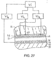
- Fig. 27
- is another schematic diagram illustrating voltages supplied to the panel shown in Figs. 16 through 19.
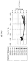
- Fig. 28
- is a graph illustrating the efficiency of panels built in accordance with the invention.
Claims (32)
- A plasma flat-panel display comprising:a first transparent substrate;at least one pair of parallel sustaining electrodes deposited upon said first substrate;a least one auxiliary electrode deposited upon said first substrate parallel to said sustaining electrodes;a layer formed from a dielectric material covering said sustaining and auxiliary electrodes;a second substrate which is hermetically sealed to said first substrate, said second substrate having a plurality of micro-voids formed in a surface thereof which is adjacent to said first substrate, said micro-voids cooperating with said first substrate to define a plurality of sub-pixels;a gas filling said micro-voids;a plurality of address electrodes Incorporated within said second substrate, each of said address electrodes corresponding to one of said sub-pixels;a first voltage supply connected to said auxiliary electrode, said first voltage supply selectively operative to apply a first voltage to said auxiliary electrode; anda second voltage supply connected to said Sustaining electrodes, said second voltage supply selectively operative to apply a second voltage to said sustaining electrodes, said second voltage being greater than said first voltage.
- A plasma flat-panel display according to claim 1 wherein said first voltage initiates a discharge between said auxiliary electrode and one of said sustaining electrodes and further wherein said second voltage causes said discharge to extend to the other of said sustaining electrodes.
- A plasma flat-panel display according to claim 2 further including a voltage supply control device connected to said first and second voltage supplies, said voltage control device operable to cause said second voltage supply to apply said second voltage to said sustaining electrodes after said first voltage is applied between said auxiliary electrode and said sustaining electrode.
- A plasma flat-panel display according to claim 2 further including a voltage supply control device connected to said first and second voltage supplies, said voltage control device operable to cause said second voltage supply to apply said second voltage to said sustaining electrodes simultaneously with the application of said first voltage between said auxiliary electrode and said sustaining electrode.
- A plasma flat-panel display according to claim 2 further including a voltage supply control device connected to said first and second voltage supplies, said voltage control device operable to cause said second voltage supply to apply said second voltage to said sustaining electrodes before said first voltage is applied between said auxiliary electrode and said sustaining electrode.
- A plasma flat-panel display according to claim 2 wherein the voltage applied to said auxiliary electrode is subsequently changed to control the depth of said discharge within a corresponding one of said micro-voids.
- A plasma flat-panel display according to claim 6 wherein said voltage applied to said auxiliary electrode is reversed to urge said discharge deep into said corresponding one of said micro-voids, whereby the illumination of the associated sub-pixel is enhanced.
- A plasma flat-panel display according to claim 6 further including a second auxiliary electrode, said second auxiliary electrode having a voltage applied thereto to further control the depth of said discharge within a corresponding one of said micro-voids.
- A plasma flat-panel display according to claim 1 including a pair of auxiliary electrodes positioned between said sustaining electrodes with said first voltage applied to said auxiliary electrodes to initiate a discharge between said auxiliary electrodes and said second voltage applied to said sustaining electrodes to extend said discharge between said sustaining electrodes.
- A plasma flat-panel display according to claim 9 further including a voltage supply control device connected to said first and second voltage supplies, said voltage control device operable to cause said second voltage supply to apply said second voltage to said sustaining electrodes after said first voltage is applied to said auxiliary electrodes.
- A plasma flat-panel display according to claim 9 further including a voltage supply control device connected to said first and second voltage supplies, said voltage control device operable to cause said second voltage supply to apply said second voltage to said sustaining electrodes simultaneously with the application of said first voltage to said auxiliary electrodes.
- A plasma flat-panel display according to claim 9 further including a voltage supply control device connected to said first and second voltage supplies, said voltage control device operable to cause said second voltage supply to apply said second voltage to said sustaining electrodes before said first voltage is applied to said auxiliary electrodes.
- A plasma flat-panel display according to claim 9 wherein the voltage applied to said auxiliary electrodes is subsequently changed to urge said control the depth to which the discharge extends into a corresponding one of said micro-voids.
- A plasma fiat-panel display comprising:a first transparent substrate;at least one pair of parallel sustaining electrodes deposited upon said first substrate;a least one auxiliary electrode deposited upon said first substrate parallel to said sustaining electrodes;a layer formed from a dielectric material covering said sustaining and auxiliary electrodes;a second substrate which is hermetically sealed to said first substrate, said second substrate having a plurality of micro-voids formed in a surface thereof which is adjacent to said first substrate, said micro-voids cooperating with said first substrate to define a plurality of sub-pixels;a gas filling said micro-voids;a plurality of address electrodes incorporated within said second substrate, each of said address electrodes corresponding to one of said sub-pixels;a first voltage supply connected between said one of said sustaining electrodes and one of said address electrodes, said first voltage supply selectively operative to apply a first voltage to said address electrode, whereby a discharge is initiated between said sustaining electrode and said address electrode;a second voltage supply connected to said auxiliary electrode, said second voltage supply selectively operative to apply a second voltage to said auxiliary electrode, whereby said discharge is redirected toward said auxiliary electrode; anda third voltage supply connected to said sustaining electrodes, said third voltage supply selectively operative to apply a third voltage to said sustaining electrodes, said third voltage being greater than said second voltage, whereby said discharge is extended to the other of said sustaining electrodes.
- A plasma flat-panel display according to claim 14 wherein said voltages establish a discharge between said sustaining electrodes and further wherein the voltage applied to said auxiliary electrode is subsequently changed to control the depth of said discharge into a corresponding one of said micro-voids.
- A plasma flat-panel display according to claim 15 further including a voltage supply control device connected to said voltage supplies, said voltage control device operable to cause said second voltage supplies to sequentially apply voltages to associated electrodes to establish a discharge between said sustaining electrodes.
- A plasma flat-panel display according to claim 1 further including an electron emissive surface layer covering said dielectric layer.
- A plasma flat-panel display according to claim 17 wherein said electron emissive layer is formed from a first electron emissive material having a first gamma and a second electron emissive material having a second gamma, said first gamma being greater than said second gamma, with said first electron emissive material being adjacent to said sustaining electrodes and said second electron emissive material being adjacent to said auxiliary electrode, such that at least one of said sustaining electrodes will preferentially function as a cathode relative to said auxiliary electrode.
- A plasma flat-panel display according to claim 17 further including a phosphor material deposited within each micro-void and associated with said address electrodes.
- A plasma flat-panel display according to claim 19 wherein said pair of parallel sustaining electrodes is a first pair of sustaining electrodes and further wherein a second pair of parallel sustaining electrodes is deposited upon said first substrate parallel to said first pair of sustaining electrodes with said auxiliary electrode disposed between said first and second pair of sustaining electrodes.
- A plasma flat-panel display according to claim 19 wherein said auxiliary electrode is a first auxiliary electrode and further wherein a second auxiliary electrode is deposited upon said first substrate parallel to said sustaining electrode, said first and second auxiliary electrodes each having a width and being disposed between said sustaining electrodes with said auxiliary electrodes separated by a distance which is greater than said width of said auxiliary electrodes.
- A plasma flat-panel display according to claim 21 wherein said first and second auxiliary electrodes are centered between said sustaining electrodes.
- A plasma flat-panel display according to claim 22 wherein the spacing of said auxiliary electrodes is within the range of 100 to 400 microns.
- A plasma flat display panel according to claim 21 wherein said first auxiliary electrode is adjacent to one of said sustaining electrodes and said second auxiliary electrode is adjacent to the other of said sustaining electrodes.
- A plasma flat-panel display according to claim 19 further including a layer of insulating film deposited upon said surface of said electron emissive layer and at least one electrically conductive surface pad located upon the surface of said insulating film in association with a corresponding sustaining electrode.
- A method of operating a plasma flat-panel display comprising the steps of:(a) providing a display including a first transparent substrate having at least one pair of parallel sustaining electrodes deposited thereupon and at least one auxiliary electrode deposited thereupon parallel to the sustaining electrodes, a layer formed from a dielectric material covering the sustaining and auxiliary electrodes, a second substrate which is hermetically sealed to the first substrate, the second substrate having a plurality of micro-voids formed in a surface thereof which is adjacent to the first substrate, the micro-voids generally perpendicular to the sustaining and auxiliary electrodes and cooperating with the first substrate to define a plurality of sub-pixels, a gas filling the micro-voids; and a plurality of address electrodes incorporated within the second substrate, each of the address electrodes corresponding to one of the sub-pixels;(b) applying a first voltage to the auxiliary electrode of sufficient magnitude to inject a charge of electrons between the auxiliary electrode and one of the associated sustaining electrodes; and(c) applying a second voltage, which is greater than the first voltage, to the sustaining electrodes to cause a discharge between the sustaining electrodes.
- A method according to claim 26 wherein the display further includes an electron emissive surface layer covering the dielectric layer, the electron emissive layer being formed from a first electron emissive material having a first gamma and a second electron emissive material having a second gamma, the first gamma being greater than the second gamma, with the first electron emissive material being adjacent to the sustaining electrodes and the second electron emissive material being adjacent to the auxiliary electrode, such that at least one of the sustaining electrodes will preferentially function as a cathode relative to the auxiliary electrode.
- A method according to claim 26 further including, subsequent to step (c), applying a third voltage to the address electrodes to control the discharge between the sustaining electrodes.
- A method according to claim 28 wherein the first and second voltages are alternating voltages.
- A method of operating a plasma flat-panel display comprising the steps of:(a) providing a display including a first transparent substrate having at least one pair of parallel sustaining electrodes deposited thereupon and a pair of parallel auxiliary electrodes deposited thereupon between and parallel to the sustaining electrodes, a layer formed from a dielectric material covering the sustaining and auxiliary electrodes, a second substrate which is hermetically sealed to the first substrate, the second substrate having a plurality of micro-voids formed in a surface thereof which is adjacent to the first substrate, the micro-voids generally perpendicular to the sustaining and auxiliary electrodes and cooperating with the first substrate to define a plurality of sub-pixels, a gas filling the micro-voids; and a plurality of address electrodes incorporated within the second Substrate, each of the address electrodes corresponding to one of the stab-pixels;(b) applying a first voltage to the auxiliary electrodes of sufficient magnitude to inject a charge of electrons between the associated sustaining electrodes; and(c) applying a second voltage, which is greater than the first voltage, to the sustaining electrodes to cause a discharge between the sustaining electrodes.
- A method according to claim 30 wherein the auxiliary electrodes are centered between the sustaining electrodes.
- A method according to claim 30 wherein one of the pair of auxiliary electrodes is adjacent to one of the sustaining electrodes and the other of the pair of auxiliary electrodes is adjacent to the other of sustaining electrodes.
Applications Claiming Priority (6)
| Application Number | Priority Date | Filing Date | Title |
|---|---|---|---|
| US376130 | 1999-08-17 | ||
| US09/376,130 US6459201B1 (en) | 1999-08-17 | 1999-08-17 | Flat-panel display with controlled sustaining electrodes |
| US16846999P | 1999-12-01 | 1999-12-01 | |
| US168469P | 1999-12-01 | ||
| US629118 | 2000-07-31 | ||
| US09/629,118 US6597120B1 (en) | 1999-08-17 | 2000-07-31 | Flat-panel display with controlled sustaining electrodes |
Publications (2)
| Publication Number | Publication Date |
|---|---|
| EP1077466A2 true EP1077466A2 (en) | 2001-02-21 |
| EP1077466A3 EP1077466A3 (en) | 2007-11-21 |
Family
ID=27389529
Family Applications (1)
| Application Number | Title | Priority Date | Filing Date |
|---|---|---|---|
| EP00117638A Withdrawn EP1077466A3 (en) | 1999-08-17 | 2000-08-16 | Flat-panel display with controlled sustaining electrodes |
Country Status (6)
| Country | Link |
|---|---|
| US (1) | US6597120B1 (en) |
| EP (1) | EP1077466A3 (en) |
| JP (1) | JP2001195985A (en) |
| KR (1) | KR100739480B1 (en) |
| CN (1) | CN1179315C (en) |
| MX (1) | MXPA00007975A (en) |
Cited By (3)
| Publication number | Priority date | Publication date | Assignee | Title |
|---|---|---|---|---|
| KR100453161B1 (en) * | 2001-10-24 | 2004-10-15 | 엘지전자 주식회사 | Plasma Display Panel and Driving Method Thereof and Fabricating Method of lower Plate Thereof |
| EP1630846A1 (en) * | 2004-08-24 | 2006-03-01 | Samsung SDI Co., Ltd. | Plasma display panel |
| EP1522987A3 (en) * | 2003-10-06 | 2006-08-23 | Lg Electronics Inc. | Method of driving a plasma display panel |
Families Citing this family (12)
| Publication number | Priority date | Publication date | Assignee | Title |
|---|---|---|---|---|
| US6597120B1 (en) * | 1999-08-17 | 2003-07-22 | Lg Electronics Inc. | Flat-panel display with controlled sustaining electrodes |
| KR20020035699A (en) * | 2000-11-07 | 2002-05-15 | 구자홍 | Plasma display panel and driving method thereof |
| KR100483988B1 (en) | 2001-11-29 | 2005-04-15 | 삼성에스디아이 주식회사 | Method of Varying Transmittance in transparent conductive film |
| JP4251389B2 (en) * | 2002-06-28 | 2009-04-08 | 株式会社日立プラズマパテントライセンシング | Driving device for plasma display panel |
| US20070171149A1 (en) * | 2003-06-23 | 2007-07-26 | Shinichiro Hashimoto | Plasma display panel apparatus and method of driving the same |
| US7511426B2 (en) * | 2004-04-22 | 2009-03-31 | The Board Of Trustees Of The University Of Illinois | Microplasma devices excited by interdigitated electrodes |
| US7573202B2 (en) * | 2004-10-04 | 2009-08-11 | The Board Of Trustees Of The University Of Illinois | Metal/dielectric multilayer microdischarge devices and arrays |
| US7477017B2 (en) | 2005-01-25 | 2009-01-13 | The Board Of Trustees Of The University Of Illinois | AC-excited microcavity discharge device and method |
| JPWO2006080128A1 (en) * | 2005-01-31 | 2008-08-07 | 株式会社ティーティーティー | Discharge type display device |
| KR100741118B1 (en) * | 2006-02-22 | 2007-07-19 | 삼성에스디아이 주식회사 | Plasma display panel |
| WO2007146279A2 (en) * | 2006-06-12 | 2007-12-21 | The Board Of Trustees Of The University Of Illinois | Low voltage microcavity plasma device and addressable arrays |
| CN106714434B (en) * | 2015-07-17 | 2024-04-09 | 核工业西南物理研究院 | Paired electrode coplanar discharge plasma generating device |
Family Cites Families (36)
| Publication number | Priority date | Publication date | Assignee | Title |
|---|---|---|---|---|
| US3559190A (en) | 1966-01-18 | 1971-01-26 | Univ Illinois | Gaseous display and memory apparatus |
| BE755591Q (en) | 1967-11-24 | 1971-02-15 | Owens Illinois Inc | GASEOUS DISCHARGE MEMORIZATION AND REPRODUCTION DEVICE AND ITS OPERATING MODE |
| US4723093A (en) | 1968-10-02 | 1988-02-02 | Owens-Illinois Television Products Inc. | Gas discharge device |
| NL7016929A (en) | 1970-11-19 | 1972-05-24 | ||
| NL7317435A (en) | 1973-12-20 | 1975-06-24 | Philips Nv | GAS DISCHARGE PANEL. |
| US4494038A (en) | 1975-03-10 | 1985-01-15 | Owens-Illinois, Inc. | Gas discharge device |
| JPS5263663A (en) | 1975-11-19 | 1977-05-26 | Fujitsu Ltd | Gas electric discharge panel |
| DE3206104A1 (en) | 1982-02-19 | 1983-09-01 | Bayer Ag, 5090 Leverkusen | VIBRATION SEPARATING SCREEN ON AGITATOR BALL MILLS |
| US4638218A (en) | 1983-08-24 | 1987-01-20 | Fujitsu Limited | Gas discharge panel and method for driving the same |
| EP0157248B1 (en) | 1984-03-19 | 1992-06-03 | Fujitsu Limited | Method for driving a gas discharge panel |
| JPS6161341A (en) | 1984-08-31 | 1986-03-29 | Fujitsu Ltd | Gas discharge panel |
| US5086297A (en) | 1988-06-14 | 1992-02-04 | Dai Nippon Insatsu Kabushiki Kaisha | Plasma display panel and method of forming fluorescent screen thereof |
| KR910020783A (en) | 1990-05-25 | 1991-12-20 | 김정배 | Plasma Display Panel and Manufacturing Method Thereof |
| KR920004143B1 (en) | 1990-07-04 | 1992-05-25 | 삼성전관 주식회사 | Plasma display panel |
| JP3013470B2 (en) | 1991-02-20 | 2000-02-28 | ソニー株式会社 | Image display device |
| EP0554172B1 (en) | 1992-01-28 | 1998-04-29 | Fujitsu Limited | Color surface discharge type plasma display device |
| US5828356A (en) | 1992-08-21 | 1998-10-27 | Photonics Systems Corporation | Plasma display gray scale drive system and method |
| US5469021A (en) | 1993-06-02 | 1995-11-21 | Btl Fellows Company, Llc | Gas discharge flat-panel display and method for making the same |
| JP3394799B2 (en) | 1993-09-13 | 2003-04-07 | パイオニア株式会社 | Plasma display device |
| JP2581465B2 (en) * | 1994-09-28 | 1997-02-12 | 日本電気株式会社 | Plasma display panel and driving method thereof |
| JP2671870B2 (en) * | 1995-05-02 | 1997-11-05 | 日本電気株式会社 | Plasma display panel and driving method thereof |
| JP2716013B2 (en) | 1995-08-11 | 1998-02-18 | 日本電気株式会社 | Color plasma display panel and method of manufacturing the same |
| RU2089966C1 (en) * | 1995-11-22 | 1997-09-10 | Научно-производственная компания "Орион-Плазма" - Совместная акционерная компания закрытого типа | Ag gaseous-discharge display panel with reversing surface discharge |
| JPH09245627A (en) * | 1996-03-07 | 1997-09-19 | Mitsubishi Electric Corp | Gas discharge display device, manufacturing method thereof and panel driving method thereof |
| US5723945A (en) | 1996-04-09 | 1998-03-03 | Electro Plasma, Inc. | Flat-panel display |
| JPH1038688A (en) | 1996-07-24 | 1998-02-13 | Nikon Corp | Spectrophotometer |
| JP3775703B2 (en) | 1996-08-28 | 2006-05-17 | タイコエレクトロニクスアンプ株式会社 | Flexible circuit board connector |
| KR19980046358A (en) * | 1996-12-12 | 1998-09-15 | 엄길용 | Plasma Display Panel Structure and Its Driving Method |
| US6448946B1 (en) | 1998-01-30 | 2002-09-10 | Electro Plasma, Inc. | Plasma display and method of operation with high efficiency |
| RU2120154C1 (en) * | 1997-03-28 | 1998-10-10 | Совместное закрытое акционерное общество "Научно-производственная компания "ОРИОН-ПЛАЗМА" | Ac surface-discharge gas panel and its control technique |
| JPH10333636A (en) * | 1997-03-31 | 1998-12-18 | Mitsubishi Electric Corp | Plasma display panel |
| JP2001039822A (en) * | 1999-07-28 | 2001-02-13 | Mikimoto Pharmaceut Co Ltd | Elastase inhibitor |
| US6597120B1 (en) * | 1999-08-17 | 2003-07-22 | Lg Electronics Inc. | Flat-panel display with controlled sustaining electrodes |
| US6459201B1 (en) | 1999-08-17 | 2002-10-01 | Lg Electronics Inc. | Flat-panel display with controlled sustaining electrodes |
| JP2001099554A (en) * | 1999-09-28 | 2001-04-13 | Sanyo Electric Co Ltd | Refrigerator |
| KR100509601B1 (en) * | 2000-04-28 | 2005-08-22 | 삼성에스디아이 주식회사 | Plasma display panel having the auxiliary electrodes for providing priming electron |
-
2000
- 2000-07-31 US US09/629,118 patent/US6597120B1/en not_active Expired - Fee Related
- 2000-08-16 MX MXPA00007975A patent/MXPA00007975A/en unknown
- 2000-08-16 EP EP00117638A patent/EP1077466A3/en not_active Withdrawn
- 2000-08-16 CN CNB001234447A patent/CN1179315C/en not_active Expired - Fee Related
- 2000-08-17 KR KR1020000047486A patent/KR100739480B1/en not_active Expired - Fee Related
- 2000-08-17 JP JP2000247710A patent/JP2001195985A/en active Pending
Cited By (6)
| Publication number | Priority date | Publication date | Assignee | Title |
|---|---|---|---|---|
| KR100453161B1 (en) * | 2001-10-24 | 2004-10-15 | 엘지전자 주식회사 | Plasma Display Panel and Driving Method Thereof and Fabricating Method of lower Plate Thereof |
| EP1522987A3 (en) * | 2003-10-06 | 2006-08-23 | Lg Electronics Inc. | Method of driving a plasma display panel |
| CN100397453C (en) * | 2003-10-06 | 2008-06-25 | Lg电子株式会社 | Method for driving plasma display |
| US7688284B2 (en) | 2003-10-06 | 2010-03-30 | Lg Electronics Inc. | Method of driving a plasma display panel |
| EP1630846A1 (en) * | 2004-08-24 | 2006-03-01 | Samsung SDI Co., Ltd. | Plasma display panel |
| US7462987B2 (en) | 2004-08-24 | 2008-12-09 | Samsung Sdi Co., Ltd. | Plasma display panel |
Also Published As
| Publication number | Publication date |
|---|---|
| US6597120B1 (en) | 2003-07-22 |
| EP1077466A3 (en) | 2007-11-21 |
| JP2001195985A (en) | 2001-07-19 |
| KR100739480B1 (en) | 2007-07-13 |
| CN1179315C (en) | 2004-12-08 |
| CN1285581A (en) | 2001-02-28 |
| KR20010039822A (en) | 2001-05-15 |
| MXPA00007975A (en) | 2002-03-11 |
Similar Documents
| Publication | Publication Date | Title |
|---|---|---|
| US5744909A (en) | Discharge display apparatus with memory sheets and with a common display electrode | |
| US6475049B2 (en) | Method of fabricating capillary electrode discharge plasma display panel device | |
| US6597120B1 (en) | Flat-panel display with controlled sustaining electrodes | |
| JP2676487B2 (en) | Discharge display device | |
| US6459201B1 (en) | Flat-panel display with controlled sustaining electrodes | |
| US6825606B2 (en) | Flat plasma display panel with independent trigger and controlled sustaining electrodes | |
| US3938135A (en) | Gas discharge display device and an improved cell therefor | |
| US6603266B1 (en) | Flat-panel display | |
| JPH03291830A (en) | Plasma display panel | |
| JP2000294144A (en) | High frequency plasma display panel and its driving method | |
| US3969650A (en) | Gas discharge display device and a novel hollow cathode therefor | |
| EP1178512A2 (en) | Flat plasma display panel with independent trigger and controlled sustaining electrodes | |
| KR100577174B1 (en) | Plasma Display Panel Using High Frequency | |
| KR100324261B1 (en) | Plasma Display Panel and Method of Driving the same | |
| JP3442107B2 (en) | Surface discharge type plasma display panel | |
| KR100293517B1 (en) | Plasma display panel and its driving method | |
| KR100357236B1 (en) | Plasma Display Panel Using High Frequency Signal And Method of Driving Thereof | |
| KR100272590B1 (en) | Plasma display panel | |
| KR100267551B1 (en) | Plasma Display Panel and Driving Method thereof | |
| KR100293514B1 (en) | High Frequency Plasma Display Panel | |
| KR200145246Y1 (en) | Plasma display device | |
| KR20020056005A (en) | Plasma display panel | |
| KR19980069574A (en) | Plasma Display Panel and Discharge Method | |
| JP2005300955A (en) | Plasma display panel and display device using the same |
Legal Events
| Date | Code | Title | Description |
|---|---|---|---|
| PUAI | Public reference made under article 153(3) epc to a published international application that has entered the european phase |
Free format text: ORIGINAL CODE: 0009012 |
|
| AK | Designated contracting states |
Kind code of ref document: A2 Designated state(s): AT BE CH CY DE DK ES FI FR GB GR IE IT LI LU MC NL PT SE |
|
| AX | Request for extension of the european patent |
Free format text: AL;LT;LV;MK;RO;SI |
|
| RIN1 | Information on inventor provided before grant (corrected) |
Inventor name: SHVYDKY, OLKSANDR Inventor name: KIM, JAE SUNG Inventor name: ANDERSON, EDWARD Inventor name: SCHERMERHORN, JERRY D. |
|
| RAP1 | Party data changed (applicant data changed or rights of an application transferred) |
Owner name: LG ELECTRONICS, INC. |
|
| PUAL | Search report despatched |
Free format text: ORIGINAL CODE: 0009013 |
|
| AK | Designated contracting states |
Kind code of ref document: A3 Designated state(s): AT BE CH CY DE DK ES FI FR GB GR IE IT LI LU MC NL PT SE |
|
| AX | Request for extension of the european patent |
Extension state: AL LT LV MK RO SI |
|
| AKX | Designation fees paid |
Designated state(s): DE FR GB NL |
|
| STAA | Information on the status of an ep patent application or granted ep patent |
Free format text: STATUS: THE APPLICATION IS DEEMED TO BE WITHDRAWN |
|
| 18D | Application deemed to be withdrawn |
Effective date: 20080522 |