EP1076241A2 - Engine control device - Google Patents
Engine control device Download PDFInfo
- Publication number
- EP1076241A2 EP1076241A2 EP00117231A EP00117231A EP1076241A2 EP 1076241 A2 EP1076241 A2 EP 1076241A2 EP 00117231 A EP00117231 A EP 00117231A EP 00117231 A EP00117231 A EP 00117231A EP 1076241 A2 EP1076241 A2 EP 1076241A2
- Authority
- EP
- European Patent Office
- Prior art keywords
- control device
- engine control
- integrated circuit
- resistor
- output
- Prior art date
- Legal status (The legal status is an assumption and is not a legal conclusion. Google has not performed a legal analysis and makes no representation as to the accuracy of the status listed.)
- Granted
Links
Images

Classifications
-
- G—PHYSICS
- G01—MEASURING; TESTING
- G01R—MEASURING ELECTRIC VARIABLES; MEASURING MAGNETIC VARIABLES
- G01R31/00—Arrangements for testing electric properties; Arrangements for locating electric faults; Arrangements for electrical testing characterised by what is being tested not provided for elsewhere
- G01R31/28—Testing of electronic circuits, e.g. by signal tracer
- G01R31/2801—Testing of printed circuits, backplanes, motherboards, hybrid circuits or carriers for multichip packages [MCP]
- G01R31/2818—Testing of printed circuits, backplanes, motherboards, hybrid circuits or carriers for multichip packages [MCP] using test structures on, or modifications of, the card under test, made for the purpose of testing, e.g. additional components or connectors
Definitions
- the present invention relates to an engine control device, and especially relates to an engine control device for screening an integrated circuit by a status that implemented in circuit board.
- a chip which is cut our from a wafer is screened after having been protected by a package, and after the initial failure that is a latent defect is removed from the integrated circuit, the chip is implemented in a circuit board.
- the integrated circuit is mounted on a circuit board by bear chip status without using the package in order to reduce mounting size or area, to improve electrical characteristics, and to achieve reduction of manufacturing cost.
- a voltage regulator is povided in the circuit board, when the voltage change over signal is output by a communication signal from an outside communications means, the voltage occurring in the resistor is amplified to be a high voltage (burn-in voltage) by an amplifier circuitry, and the screening is performed by adding said high voltage in said integrated circuit (For example, Japanese Patent Laid-open No. 09-304481 and 10-009041 are referred to).
- Japanese Patent Laid-open No. 09-304481 bulletin it is disclosed to screen by adding a burn-in voltage on the integrated circuit after mounting it, wherein the conventional equipment needs a voltage supervisory circuit and a communications means other than a voltage regulator having a resistor, an amplifier, etc. and the constitution thereof becomes to be complicated, and any particular care-and-attention is not done relating to reduction of manufacturing cost by diminution of material number of items and number of production process as a characteritic feature in a case to mount on the circuit board by the bear chip status.
- Japanese Patent Laid-open No. 10-009041 bulletin although any communications means from external is not needed, constitution of said voltage regulator and said voltage supervisory circuit are the same, Japanese Patent Laid-open No. 09-304481 bulletin does not disclose anything relating to the reduction of the manufacturing cost.
- the present invention is invented referring to such subject stated above, and an object of the present invention is to provided an engine control device having a voltage adjustment circuitry by screening a semiconductor integrated circuit mounted on a circuit board in bear chip status so as to reduce a mounting area thereof, improve electric characteristics and reduce manufacturing cost by planning a simple constitution.
- an engine control device in the present invention is characterized by comprising an integrated circuit basically such as an arithmetic processing unit etc. for processing operation of control programs, and an output voltage adjustment circuitry to switch a rated voltage to screen said integrated circuit, wherein said output voltage adjustment circuitry comprises plural resistors provided between an output side power line of said rated voltage and a gland side.
- the preswent invention is characterized in that said engine control device adds a higher voltage value than that in usual operation on said integrated circuit when screening said integrated circuit, and said output voltage adjustment circuitry is connected to an other resistor connected to said gland side and a connecting point between said plural resistors is connected to said other resistor and is connected to said constant voltage source circuitry which outputs said rated voltage to said integrated circuit.
- the present invention comprises the output voltage adjustment circuitry to switch the rated voltage to screen the integrated circuit, said output voltage adjustment circuitry being constituted with three resistors at least, all integrated circuits can be screened after being mounted by a low cost constitution without constituting a complicated circuitry, and it becomes possible to reduce manufacturing cost and to save time of screening.
- a concrete aspect of the engine control device in the present invention is characterized in that the other resistor is connected with the gland side by switching on/off.
- the concrete aspect of the engine control device in the present invention is characterized in that said other resistor is provided in external of said engine control device, or is connected to a connecting point between said plural resistors through a non-used terminal of said engine control device,
- a concrete aspect of the engine control device in the present invention is characterized in that the other resistor is provided in internal of said engine control device, or switches on/off based on a serial communication signal.
- the concrete aspect of the engine control device in the present invention is characterized in that said arithmetic processing unit has a memory device to be capable of rewriting said control program by said serial communication signal so as to switch on/off, or said arithmetic processing unit has a control program to switch over said rated voltage by said serial communication signal so as to switch on/off.
- control device in the present invention is characterized by comprising said control device comprises an integrated circuit such as an arithmetic processing unit etc. for processing operation of control programs, an output voltage adjustment means to switch a rated voltage to screen said integrated circuit, and a check means to examine characteristic of said arithmetic processing unit and said integrated circuit.
- integrated circuit such as an arithmetic processing unit etc. for processing operation of control programs
- output voltage adjustment means to switch a rated voltage to screen said integrated circuit
- check means to examine characteristic of said arithmetic processing unit and said integrated circuit.
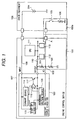
- Figure 1 is a block diagram to show first embodiment configuration of the engine control device.
- An engine control device 107 is constituted with a constant voltage source circuitry 100, an arithmetic processing unit (CPU) 111, and an integrated circuit (IC) 112, 113 etc. such as the CPU etc. and the CPU 111 and the integrated circuit 112, 113 are mounted on a circuit board in bear chip status .
- CPU arithmetic processing unit
- IC integrated circuit
- the engine control device 107 takes in a signal from a crank angle sensor ( illustration is omitted ) and detecting signals from other various sensors (illustration is omitted), and processes based on detecting signals, so as to output a driving signal to fuel injection valves (illustration is omitted) and outputs an ignition driving signal to a spark plug (illustration is omitted), and the engine control device 107 is constracted with an input circuit (illustration is omitted), an AD conversion part (illustration is omitted), a storadge device POM (illustration is omitted), and an output circuit (illustration is omitted).
- the input circuit takes in an input signal (for example, signals from a coolant temperature sensor, a crank angle sensor, and an air fuel ratio sensor etc.) and removes noise component from the input signal so as to supplyes the input signal to an AD conversion part.
- the AD conversion part converts the input signal and it is output into the CPU 111.
- the CPU 111 takes in the signal converted by the AD conversion and executes a predetermined control program stored in the ROM, thereby has a function to execute control of the device. Further, the operation result and the AD conversion result are stored temporarily in the RAM and the operation result of is output as a control output signal through the output circuit so as to be used to control the fuel injection valves.
- the engine control device 107 is connected with a check equipment (a screening equipment) 108 through a connector in order to screen the CPU 111 and the integrated circuits 112, 113, and after having screened the integrated circuits 112, 113, characteristics of the CPU 111 and the integrated circuits 112, 113 are checked so as to distinguish good or bad thereof, then, after being separated from the check instrument 108, only a good device is adopted to an actual machine as the engine control device 107.
- a check equipment a screening equipment
- the check instrument 108 is capable of supplying the battery voltage 304 to a constant voltage source circuitry 100 of the engine control device 107 through an input side power line 109, thereby the constant voltage source circuitry 100 is connected with an output voltage adjustment circuitry 150, and the output voltage adjustment circuitry 150 switches the rated voltage so as to screen the integrated circuits 112, 113.
- the constant voltage source circuitry 100 is a variable output type one and constracted with a current source 114, a reference voltage source 104, a start up circuitry 115, an error amplifier 116, and a transistor 117, and outputs a constant rated voltage (for example, 5V) to the CPU 111 and the integrated circuits 112,113 through the output side power line 110.
- a constant rated voltage for example, 5V
- the output voltage adjustment circuitry 150 switches said rated voltage as stated above so as to screen the CPU 111 and the integrated circuits 112, 113 and is constructed with resistors 101,102,106 and an electric switch 105, and the resistor 101 and the resistor 102 are connected in series between the output side power line 110 of the rated voltage and the gland side.
- the other resistor 106 to be different from the resistors 101, 102 is provided in an other output voltage adjustment circuitry 150a inside of the check equipment 108, one end thereof is connected to the gland side through the electric switch 105, and another end thereof is connected with a connecting point 103 between the resitors 101, 102, and it is connected with the resistor 102 in parallel by turning the electric switch 105 on.
- the other resistor 106 is connected with the connecting point 103 between the resistors 101, 102 through non-used terminal of the engine control device 107, and is simultaneously connected with a reference voltage source 104 of the constant voltage source circuitry 100.
- the screening for the CPU 111 and the integrated circuits 112, 113 is performed as follows.
- the battery voltage 304 is supplied to the engine control device 107 by the check equipment 108 through the input side power line 109, and the constant voltage source circuitry 100 supplys a source voltage of the usual constant rated voltage (for example, 5V) to the CPU 111 and the integrated circuits 112, 113 through output side power line 110, thereby the CPU 111 and the integrated circuits 112, 113 start to operat.
- a source voltage of the usual constant rated voltage for example, 5V
- This voltage value of the connecting point 103 in a usual time is determined according to a ratio of the resistor 101 and the resistor 102 connected in series, and the constant rated voltage is maintained by comparing the intermediate voltage value with a voltage value of the reference voltage source 104 with the error amplifier 116.
- the voltage value of the connecting point 103 (intermediate voltage value) is determined to be switched according to a ratio of the resistors 102 and 106 connected in parallel and the resistor 101 connected therewith in series, by turning the electric switch 105 of the output voltage adjustment circuitry 150, and a voltage value which is higher than that in the usual time is supplied to the CPU 111 and the integrated circuit 112, 113 through the output side power line 110 so as to screen them.
- the electric switch 105 is turned off, and the characteristic of the device is tested with the check equipment 108 after a predetermined time from the finishing, then the initial failures being a potential defect of the CPU 111 and the integrated circuit 112, 113 are removed by checking the function of the engine control device 107.
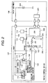
- Figure 2 is a block diagram which shows a second embodiment configuration of the engine control device, and as figure 2 shows the same construction as figure 1 besides a CPU 200 and an output voltage adjustment circuitry 250, and only the CPU 200 and the output voltage adjustment circuitry 250 will be explained in detail.
- Said CPU 200 builts in a ROM (a flash ROM) which is capable of rewriting the control program and controls the intermediate voltage of the connecting point 103 by the rewritten control program.
- the output voltage adjustment circuitry 250 is used to switch the rated voltage in order to screen the integrated circuit 112,113 and is constructed with the resistors 101, 102, 201 and the transistor 204, and the resistor 101 and the resistor 102 are is connected in series between the output side power line 110 of the rated voltage and the gland side.
- the other resistor 201 to be different from the resistors 101, 102 is provided inside of the engine control device 107, one end thereof is connected to the gland side through the electric switch 105, and one end thereof is connected with ground side of the transistor 204 and another end thereof is connected with the connecting point 103 between the resitors 101, 102, and it is connected with the resistor 102 in parallel by turning the electric switch 204 on.
- an serial communication means 203 is arranged, and the CPU 200 is switched into a write mode by being transmitted the output signal and the control program from the serial communication means 203, and simultaneouly the control program of the flash ROM in the CPU 200 is rewritten.
- the intermediate voltage value is determined according to a ratio of the resistors 101 and 102 connected in series.
- the serial communication means 203 turns on the transistor 204 and determines the voltage value of the connecting point 103 (intermediate voltage value) so as to switch it based on a ratio of the resistors 102 and 106 connected in parallel and the resistor 101 connected in series therewith , and the voltage value which is higher than that in the usual time is supplied on the CPU 200 and the integrated circuit 112, 113 through the output side power line 110 so as to screen thereof.
- the program to fix the output of the port 202 to be low level again is rewritten on the flash ROM by a serial communication means 203, thereby the transistor 204 is turned off and characteristics of the device is checked with the check equipment 108 after a predetermined time has passed, then the initial failures being a potential defect of the CPU 200 and the integrated circuit 112, 113 are removed by checking the function of the engine control device 107.
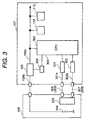
- Figure 3 is a block diagram which shows a third embodiment configuration of the engine control device, and as figure 3 shows the same construction as figure 2 besides a CPU 300 and only the CPU 300 will be explained in detail.
- the CPU 300 builts in the control program to switch a program to fix the output of the port 309 to be the low level and a program to fix the output of the port 309 to be the high level mutually so as to control the intermediate voltage of the connecting point 103.
- the output voltage adjustment circuitry 303 is constituted in the same way as output voltage adjustment circuitry 250 shown in figure 2, has the resistor 101, 102 and 201 and the transistor 204, and switches the rated voltage in order to screen the integrated circuits 112, 113.
- the resistors 101 and 102 is connected in series between the output side power line 109b of the rated voltage and the gland side.
- the one end of the other resistor 201 is connected to the gland side through the transistor 204, and the other end of the resistor 201 is connected with the connecting point 103 between the resitors 101, 102 and is connected with the resistor 102 in parallel by turning the transistor 204 on.
- a program to fix the output of the port 309 of the CPU 300 to be the low level is designated by the serial communication means 203 so as to turn the transistor 204 off
- a program to fix the output of the port 309 of the CPU 300 to be the high level is designated by the serial communication means 203 so as to turn the transistor 204 on
- the voltage value which is higher than that in the usual time is supplied to the CPU 300 and the integrated circuits 112, 113 through the output side power line 110 so as to screen them.
- the program to fix the output of the port 309 to be the low level is designated, the transistor 204 is turned off, and after the predetermined time has passed, the characteristic of the device is checked by the check equipment 108, then the initial failures being a potential defect of the integrated circuits 112, 113 are removed by checking the function of the engine control device 107.
- Figure 4 is a timing chart of operating of the engine control device shown by figure 3.
- the battery voltage 304 is applied to engine control device 107 through the input side power line 109a by using the check equipment (a screening test device) 108, and the constant voltage source circuitry 100 supplys a source voltage having the constant rated voltage (for example, 5V) in the usual time to the CPU 300 and the integrated circuit 112, 113 through the output side power line 109b so as to start to operate the CPU 300 and the integrated circuit 112, 113.
- a source voltage having the constant rated voltage for example, 5V
- the CPU 300 receives the high voltage switching designation signal 305 through the serial receiver circuit 301, the high voltage switching designation signal 305 is output by the output voltage adjustment circuitry 303 so as to turn the transistor 204 on, and the output voltage value of the constant voltage source circuitry 100 is changed to be the high voltage value (7V, for example) for the screening.
- the CPU 300 transmits a change over completion signal 307 to the communication line 302a through a serial transmitting circuit 302 and the signal 307 is returned to the check equipment 108.
- the CPU 300 receives the rated voltage change over designation signal 306 through the serial receiver circuit 301, the rated voltage change over designation signal 306 is output to the output voltage adjustment circuitry 303, the transistor 204 is turned off, and the output voltage value of the constant voltage source circuitry 100 is changed to be the rated voltage (5V, for example).
- the CPU 300 transmits the change over completion signal 308 to the communication line 302a through the serial transmitting circuit 302, and the signal 308 returned to the check equipment 108.
- the characteristic of the device is tested by the check equipment 108, and the initial failures being potential defects of the integrated circuits 112, 113 are judged by checking the function of the engine control device 107.
- the embodiment configuration in the present invention has following function based on the constitution mentioned above.
- the engine control device 107 in the first embodiment configuration of the present invention comprises the CPU 111 to operate the program, integrated circuits 112, 113, the ROM to store the program, the constant voltage source circuitry 100 to output the rated voltage to the integrated circuits 112, 113 etc. and the output voltage adjustment circuitry 150 to switch the rated voltage in order to screen the integrated circuits 112, 113 mounted on the circuit board.
- the output voltage adjustment circuitry 150 is connected to other output voltage adjustment circuitry 150a so as to connect the resistors 101, 102, 106 with the electric switch 105, the resistors 101 and 102 are connected in series between the output side power line 110 of the rated voltage and the gland sides, one end of the other resistor 106 is connected to the gland side and other end thereof is connected to the connecting point 103 of the resistors 101, 102 and the other resistor 106 is connected with the resistor 102 in parallel by turning the electric switch 105 on, and the reference voltage source 104 of the constant voltage source circuitry 100 is connected with the connecting point 103 between the resistors 101, 102 through the non-used treminal A of the engine control device 107.
- the screening of all integrated circuits 112, 113 after being mount can be performed at a time by changing the intermediate voltage of connecting point 103 without providing the complicated circuitry and the outside output signal means especially, reduction of the manufacturing cost and shortening of the time of the screening can be planned.
- the voltage value is changed for the screening, and the reduction of the power consumption can be planned by using the change of this voltage value for engine control.
- the CPU 200 builds in the ROM (flash ROM) in which the program thereof is capable of being rewritten, the program of the CPU 200 is written in by the serial communication means 203, thereby the transistor 204 of the output voltage adjustment circuitry 250 is switched on or off so as to change the intermediate voltage of the connecting point 103, and in a case of an engine control device having a limitted terminal and not having a non-used terminal A, the screening of the integrated circuits 112, 113 after mounting can be performed.
- ROM flash ROM
- the CPU 300 build in the control program to mutually switch a program to fix output of the port 309 of the CPU 300 to be in the low and a program to fix output of the port 309 to be in the high level according to the output signal from the serial communication means 203, the programs of the CPU 300 are switched by the serial communication means 203, thereby, the transistor 204 of the output voltage adjustment circuitry 303 is swtched on or off and the intermediate voltage of the connecting point 103 can not be changed, and if the engine control device does not have non-used terminal A and the CPU does not have the flash ROM, the screening of the integrated circuit 112, 113 after mounting can be performed.
- the output voltage adjustment circuitry is divided into the engine control device and the check equipment, however this circuitry may be provided as one body in the engine control device.
- the check equipment is not limitted to be used for only the engine control device, and by providing the output voltage adjustment circuitry and the characteristic check circuit as the control device of the integrated circuit mounted as the bear chip status, the creening of the integrated circuit and the function test can be performed.
- the engine control device in the present invention can perform the screening of the semiconductor integrated circuit mounted as the bear chip status on the circuit board by arranging the output voltage adjustment circuit, and reduction of the mounting area size and improvement of the electrical characteristic nature becomes possible and reduction of the manufacturing cost can be planned too by a simple constitution thereof.
Landscapes
- Engineering & Computer Science (AREA)
- Computer Hardware Design (AREA)
- Microelectronics & Electronic Packaging (AREA)
- General Engineering & Computer Science (AREA)
- Physics & Mathematics (AREA)
- General Physics & Mathematics (AREA)
- Combined Controls Of Internal Combustion Engines (AREA)
- Tests Of Electronic Circuits (AREA)
- Testing Of Individual Semiconductor Devices (AREA)
Abstract
Description
Claims (11)
- An engine control device comprising an integrated circuit (112, 113) such as an arithmetic processing unit etc. for processing operation of control programs, characterized in thatsaid engine control device (107) comprises an output voltage adjustment circuitry (150) to switch a rated voltage to screen said integrated circuit, andsaid output voltage adjustment circuitry (150) comprises plural resistors (101, 102) provided between an output side power line of said rated voltage and a gland side.
- An engine control device as defined in claim 1, said engine control device (107) being characterized in thatsaid output voltage adjustment circuitry (150) is connected to another resistor (106) connected to said gland side, anda connecting point (103) between said plural resistors (101, 102) is connected to said other resistor (106) and is connected to said constant voltage source circuitry (150) which outputs said rated voltage to said integrated circuit (112, 113).
- An engine control device as defined in claim 2, said engine control device being characterized in thatsaid other resistor (106) is connected to said gland side by change over a switch on/off (105).
- An engine control device as defined in claim 2 or 3, said engine control device (107) being characterized in that said other resistor (106) is provided outside of said engine control device (107).
- An engine control device as defined in claim 4, said engine control device (107) being characterized in that said other resistor (106) is connected to a connecting point (103) between said plural resistors through a non-connected terminal of said engine control device (107).
- An engine control device as defined in claim 2 or 3, said engine control device (107) being characterized in thatsaid other resistor (201) is provided inside of said engine control device (107).
- An engine control device as defined in claim 6, said engine control device (107) being characterized in thatsaid other resistor (201) is switched on/off by a serial communication signal.
- An engine control device as defined in claim 7, said engine control device (107) being characterized in thatsaid arithmetic processing unit has a memory device to be capable of rewriting said control program by said serial communication signal so as to switch on/off.
- An engine control device as defined in claim 7, said engine control device (107) being characterized in thatsaid arithmetic processing unit has a control program to switch over said rated voltage by said serial communicaton signal so as to switch on/off.
- An engine control device as defined in claims 1 to 9, said engine control device (107) being characterized in thatsaid engine control device (107) adds a higher voltage value than that in usual operation on said integrated circuit (112, 113) when screening said integrated circuit (112, 113).
- A control device comprising an integrated circuit (112, 113) of an arithmetic processing unit for operating a control program, comprisingan output voltage adjustment means (150) to switch over a rated voltage to screen said integrated circuit (112, 113), anda check means (108) to examine a characteristic of said arithmetic processing unit and said integrated circuit (112, 113).
Applications Claiming Priority (2)
| Application Number | Priority Date | Filing Date | Title |
|---|---|---|---|
| JP22844499 | 1999-08-12 | ||
| JP22844499A JP3585401B2 (en) | 1999-08-12 | 1999-08-12 | Engine control device |
Publications (3)
| Publication Number | Publication Date |
|---|---|
| EP1076241A2 true EP1076241A2 (en) | 2001-02-14 |
| EP1076241A3 EP1076241A3 (en) | 2003-10-29 |
| EP1076241B1 EP1076241B1 (en) | 2005-11-30 |
Family
ID=16876598
Family Applications (1)
| Application Number | Title | Priority Date | Filing Date |
|---|---|---|---|
| EP00117231A Expired - Lifetime EP1076241B1 (en) | 1999-08-12 | 2000-08-11 | Engine control device |
Country Status (4)
| Country | Link |
|---|---|
| US (1) | US6781362B1 (en) |
| EP (1) | EP1076241B1 (en) |
| JP (1) | JP3585401B2 (en) |
| DE (1) | DE60024369T2 (en) |
Families Citing this family (5)
| Publication number | Priority date | Publication date | Assignee | Title |
|---|---|---|---|---|
| US7802141B2 (en) * | 2004-03-05 | 2010-09-21 | Denso Corporation | Semiconductor device having one-chip microcomputer and over-voltage application testing method |
| JP2006019663A (en) * | 2004-07-05 | 2006-01-19 | Denso Corp | Bare chip set, bare chip inspection method, bare chip, and bare chip mounted circuit board |
| KR100800489B1 (en) * | 2006-12-21 | 2008-02-04 | 삼성전자주식회사 | Device for providing reference voltage of semiconductor integrated circuit |
| JP2010002194A (en) * | 2008-06-18 | 2010-01-07 | Shibasoku:Kk | Testing device and testing method |
| CN103105571B (en) * | 2013-01-24 | 2015-05-06 | 东南大学 | Simulated measurement method of current characteristics of insulated gate bipolar transistor |
Family Cites Families (11)
| Publication number | Priority date | Publication date | Assignee | Title |
|---|---|---|---|---|
| US5146172A (en) * | 1990-08-15 | 1992-09-08 | Sundstrand Corp. | Engine identification system |
| US5200696A (en) * | 1990-09-10 | 1993-04-06 | Ltx Corporation | Test system apparatus with Schottky diodes with programmable voltages |
| US5339028A (en) * | 1992-07-23 | 1994-08-16 | Texas Instruments Incorporated | Test circuit for screening parts |
| JP2922733B2 (en) * | 1992-10-14 | 1999-07-26 | 三菱電機株式会社 | Hybrid integrated circuit device |
| JPH07287603A (en) * | 1994-04-19 | 1995-10-31 | Hitachi Ltd | Engine controller |
| JP3301874B2 (en) * | 1994-12-19 | 2002-07-15 | 松下電器産業株式会社 | Semiconductor device and inspection method thereof |
| US5731707A (en) * | 1996-04-17 | 1998-03-24 | Mitutoyo Corporation | Method and apparatus for synthesizing spatial waveforms in an electronic position encoder |
| JPH09304481A (en) * | 1996-05-17 | 1997-11-28 | Nissan Motor Co Ltd | On-board screening equipment |
| JPH109041A (en) | 1996-06-24 | 1998-01-13 | Nissan Motor Co Ltd | In-vehicle electronic unit |
| JPH1136974A (en) * | 1997-07-24 | 1999-02-09 | Mitsubishi Electric Corp | Vehicle control device |
| JP3392029B2 (en) * | 1997-12-12 | 2003-03-31 | 株式会社アドバンテスト | IC tester voltage applied current measuring circuit |
-
1999
- 1999-08-12 JP JP22844499A patent/JP3585401B2/en not_active Expired - Fee Related
-
2000
- 2000-08-11 US US09/636,029 patent/US6781362B1/en not_active Expired - Fee Related
- 2000-08-11 DE DE60024369T patent/DE60024369T2/en not_active Expired - Lifetime
- 2000-08-11 EP EP00117231A patent/EP1076241B1/en not_active Expired - Lifetime
Also Published As
| Publication number | Publication date |
|---|---|
| DE60024369D1 (en) | 2006-01-05 |
| JP2001051023A (en) | 2001-02-23 |
| EP1076241B1 (en) | 2005-11-30 |
| EP1076241A3 (en) | 2003-10-29 |
| DE60024369T2 (en) | 2006-08-03 |
| JP3585401B2 (en) | 2004-11-04 |
| US6781362B1 (en) | 2004-08-24 |
Similar Documents
| Publication | Publication Date | Title |
|---|---|---|
| US6885095B2 (en) | Test circuit and multi-chip package type semiconductor device having the test circuit | |
| US7913002B2 (en) | Test apparatus, configuration method, and device interface | |
| CN102770778A (en) | Method for testing an integrated circuit | |
| EP1076241A2 (en) | Engine control device | |
| KR102921457B1 (en) | Reconfigurable system-on-chip | |
| JPH09304481A (en) | On-board screening equipment | |
| KR100310971B1 (en) | method for testing a wire harness and system for performming the same | |
| US20110032036A1 (en) | Performance tuning using encoded performance parameter information | |
| US5367263A (en) | Semiconductor integrated circuit device and test method therefor | |
| US20080094096A1 (en) | Semiconductor testing equipment and semiconductor testing method | |
| JP2005173697A (en) | Semiconductor integrated circuit device and microcomputer development support device | |
| KR100369022B1 (en) | Integrated circuit with a self-test device | |
| US20080028104A1 (en) | Semiconductor device and operation control method of semiconductor device | |
| JPH10115662A (en) | Test circuit for semiconductor integrated logic circuit | |
| US20120078461A1 (en) | Control apparatus for vehicular electric component | |
| JP3194040B2 (en) | IC module | |
| US6911815B2 (en) | Semiconductor test system and method of operating the same | |
| JP3852688B2 (en) | Integrated circuit with overheat detection circuit, integrated circuit with temperature rise avoidance control means, and burn-in test method thereof | |
| KR100549342B1 (en) | Apparatus and method for sorting failure of power supply of mobile communication terminal | |
| US20100052767A1 (en) | Semiconductor module | |
| JP2001100837A (en) | Input/output connection inspecting method for electronic controller, and microcomputer | |
| JP3697843B2 (en) | Microcomputer inspection method | |
| US7403437B2 (en) | ROM test method and ROM test circuit | |
| JP2000124273A (en) | Semiconductor integrated circuit and method for inspecting electrical characteristics thereof | |
| JPH04299565A (en) | Ic chip |
Legal Events
| Date | Code | Title | Description |
|---|---|---|---|
| PUAI | Public reference made under article 153(3) epc to a published international application that has entered the european phase |
Free format text: ORIGINAL CODE: 0009012 |
|
| AK | Designated contracting states |
Kind code of ref document: A2 Designated state(s): AT BE CH CY DE DK ES FI FR GB GR IE IT LI LU MC NL PT SE |
|
| AX | Request for extension of the european patent |
Free format text: AL;LT;LV;MK;RO;SI |
|
| PUAL | Search report despatched |
Free format text: ORIGINAL CODE: 0009013 |
|
| AK | Designated contracting states |
Kind code of ref document: A3 Designated state(s): AT BE CH CY DE DK ES FI FR GB GR IE IT LI LU MC NL PT SE |
|
| AX | Request for extension of the european patent |
Extension state: AL LT LV MK RO SI |
|
| RIC1 | Information provided on ipc code assigned before grant |
Ipc: 7G 06F 11/00 B Ipc: 7G 01R 31/317 B Ipc: 7G 06F 15/78 B Ipc: 7G 01R 31/00 A |
|
| 17P | Request for examination filed |
Effective date: 20040420 |
|
| 17Q | First examination report despatched |
Effective date: 20040528 |
|
| AKX | Designation fees paid |
Designated state(s): DE FR GB IT |
|
| GRAP | Despatch of communication of intention to grant a patent |
Free format text: ORIGINAL CODE: EPIDOSNIGR1 |
|
| GRAS | Grant fee paid |
Free format text: ORIGINAL CODE: EPIDOSNIGR3 |
|
| GRAA | (expected) grant |
Free format text: ORIGINAL CODE: 0009210 |
|
| AK | Designated contracting states |
Kind code of ref document: B1 Designated state(s): DE IT |
|
| RAP1 | Party data changed (applicant data changed or rights of an application transferred) |
Owner name: HITACHI CAR ENGINEERING CO., LTD. Owner name: HITACHI, LTD. |
|
| REF | Corresponds to: |
Ref document number: 60024369 Country of ref document: DE Date of ref document: 20060105 Kind code of ref document: P |
|
| PLBE | No opposition filed within time limit |
Free format text: ORIGINAL CODE: 0009261 |
|
| STAA | Information on the status of an ep patent application or granted ep patent |
Free format text: STATUS: NO OPPOSITION FILED WITHIN TIME LIMIT |
|
| 26N | No opposition filed |
Effective date: 20060831 |
|
| PGFP | Annual fee paid to national office [announced via postgrant information from national office to epo] |
Ref country code: DE Payment date: 20090824 Year of fee payment: 10 |
|
| PGFP | Annual fee paid to national office [announced via postgrant information from national office to epo] |
Ref country code: IT Payment date: 20090721 Year of fee payment: 10 |
|
| PG25 | Lapsed in a contracting state [announced via postgrant information from national office to epo] |
Ref country code: IT Free format text: LAPSE BECAUSE OF NON-PAYMENT OF DUE FEES Effective date: 20100811 |
|
| REG | Reference to a national code |
Ref country code: DE Ref legal event code: R119 Ref document number: 60024369 Country of ref document: DE Effective date: 20110301 |
|
| PG25 | Lapsed in a contracting state [announced via postgrant information from national office to epo] |
Ref country code: DE Free format text: LAPSE BECAUSE OF NON-PAYMENT OF DUE FEES Effective date: 20110301 |