EP1075106A2 - Receiver for signals in a discontinuous flow and corresponding receiving process - Google Patents
Receiver for signals in a discontinuous flow and corresponding receiving process Download PDFInfo
- Publication number
- EP1075106A2 EP1075106A2 EP00114345A EP00114345A EP1075106A2 EP 1075106 A2 EP1075106 A2 EP 1075106A2 EP 00114345 A EP00114345 A EP 00114345A EP 00114345 A EP00114345 A EP 00114345A EP 1075106 A2 EP1075106 A2 EP 1075106A2
- Authority
- EP
- European Patent Office
- Prior art keywords
- signal
- packet
- phase
- discontinuous flow
- bit rate
- Prior art date
- Legal status (The legal status is an assumption and is not a legal conclusion. Google has not performed a legal analysis and makes no representation as to the accuracy of the status listed.)
- Withdrawn
Links
Images
Classifications
-
- H—ELECTRICITY
- H04—ELECTRIC COMMUNICATION TECHNIQUE
- H04L—TRANSMISSION OF DIGITAL INFORMATION, e.g. TELEGRAPHIC COMMUNICATION
- H04L7/00—Arrangements for synchronising receiver with transmitter
- H04L7/02—Speed or phase control by the received code signals, the signals containing no special synchronisation information
- H04L7/033—Speed or phase control by the received code signals, the signals containing no special synchronisation information using the transitions of the received signal to control the phase of the synchronising-signal-generating means, e.g. using a phase-locked loop
- H04L7/0337—Selecting between two or more discretely delayed clocks or selecting between two or more discretely delayed received code signals
- H04L7/0338—Selecting between two or more discretely delayed clocks or selecting between two or more discretely delayed received code signals the correction of the phase error being performed by a feed forward loop
-
- H—ELECTRICITY
- H04—ELECTRIC COMMUNICATION TECHNIQUE
- H04L—TRANSMISSION OF DIGITAL INFORMATION, e.g. TELEGRAPHIC COMMUNICATION
- H04L7/00—Arrangements for synchronising receiver with transmitter
- H04L7/0079—Receiver details
- H04L7/0087—Preprocessing of received signal for synchronisation, e.g. by code conversion, pulse generation or edge detection
-
- H—ELECTRICITY
- H04—ELECTRIC COMMUNICATION TECHNIQUE
- H04L—TRANSMISSION OF DIGITAL INFORMATION, e.g. TELEGRAPHIC COMMUNICATION
- H04L7/00—Arrangements for synchronising receiver with transmitter
- H04L7/02—Speed or phase control by the received code signals, the signals containing no special synchronisation information
- H04L7/027—Speed or phase control by the received code signals, the signals containing no special synchronisation information extracting the synchronising or clock signal from the received signal spectrum, e.g. by using a resonant or bandpass circuit
Definitions
- the present invention tackles the problem of receiving signals in a discontinuous flow and with a high bit rate. This problem arises, for example, within the switching nodes of packet-switched optical networks.
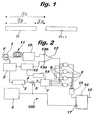
- a signal corresponding to a flow of data of the type described above is shown schematically in Figure 1.
- this is a flow of data at a high bit rate (fc), transmitted from a remote system along an optical fibre, for example, and intended to be received in a receiving device.
- the data flow in question is structured in packets with a duration of Tp, separated by "guard times", denoted by Tg, in which no data are transmitted.
- Ts Tp + Tg .
- the object of the present invention is to provide a device capable of enabling data flows of the type described above to be received in a precise and reliable way.
- this object is achieved by means of a receiver having the characteristics called for in the following claims.
- the invention also relates to the corresponding process of reception.
- the solution according to the invention provides for the execution, at the time of reception of each packet, of a kind of "pre-reading" of at least part of the packet, with the purpose of acquiring the information relating to the phase (and, preferably, also the mean signal power) of each packet.
- the information thus acquired is then used for the execution of the actual reading operation.
- a receiver according to the invention is shown here by way of example in the form of an optical receiver. This is, therefore, a device intended to receive an optical signal (having the characteristics described previously with reference to Figure 1) from an optical fibre F.
- An in-fibre power splitter 1 (of a known type), associated with the output end of the fibre F, diverts from the fibre a portion (for example 10%) of the transmitted signal and sends it to a narrow band receiver 2.
- narrow band receiver here denotes in general an optical-electrical converter whose sensitivity curve is concentrated around a frequency value equal to a frequency ft equal to the (known) frequency of the clock which generates the packet in transmission.
- phase locked loop circuit 3 After a settling time Ta following the start of each packet (the total Ta is generally shorter than Tp), the phase locked loop circuit 3 generates at a corresponding output 4 a signal whose phase is locked to the phase of the signal generated by the remote transmitter with the frequency ft, the identifier of the bit rate fc.
- This signal is sent to a mixer 5 together with a signal generated at a frequency fr by a local clock 6.
- the values of ft and fr are identical or at least very close to each other, and therefore the output signal from the mixer 5 is (at least within each packet) proportional to the phase difference ⁇ between the two signals brought to the input of the mixer 5.
- the signal indicating the phase difference ⁇ is then supplied to an analogue-digital converter 7 which generates, on corresponding output lines indicated by a, b, c and d, logical signals corresponding to the value of ⁇ .
- the aforesaid logical signals are generated - in a known way - according to the following table.
- the one of the outputs a, b, c and d of the device 7 which has the logical value "1" (while all three of the other outputs have the logical value "0") identifies the quadrant in which the phase difference ⁇ is located.
- the components indicated as a whole by 8 consist of logical gates, their number being equal to the separate values which can be taken by the signal (lines a, b, c, d) emitted by the converter 7.
- the main optical signal is propagated along a portion of fibre 11 of length L such that it introduces a delay ⁇ into the main signal.
- the length L is chosen in such a way that ⁇ is at least equal to, and therefore greater, than, both Ta (the settling time of the PLL 3 from the start of the packet) and a value Ti defining the settling time of a detector circuit 12.
- the function of the detector circuit 12 (shown here as being designed to receive the output of the narrow band receiver 2 at its input, but actually capable of being integrated into the receiver 2 itself) is to generate and maintain throughout the duration of the packet a signal corresponding to the mean power value of the received signal.
- This has the purpose of permitting the fixing of the threshold of discrimination 13a of a comparator circuit 13 which receives, at 13b, the electrical signal deriving from the conversion, carried out in the receiver device 10, of the main optical signal delayed by its passage along the fibre 11.
- the detector 12 is provided in order to enable the comparator circuit 13 to discriminate the values of the signal arriving from the receiver 10 according to an adaptive threshold related to the mean value of the signal within each packet.
- the device 10 essentially consists of a wide band receiver capable of carrying out a correct action of converting the main optical signal including the modulation component. In all of this it differs from the omologous device 2, which is essentially a narrow band receiver centred on the frequency at which the phase locking is to be carried out.
- the reference 14 indicates a generator, of a known type, capable of generating (according to a command arriving from the exterior or generated, in a known way, in the device 100) a signal such that the detector 12 and the converter 7 are reset when the reception of a packet is complete, to prepare them for the reception of the next packet.
- the output signal from the comparator 13 is then sent to the inputs of the logical gates 8 in a direct version (supplied to the first of the gates 8) and in the form of three replicas altered by incremental phase shifts or delays applied to the signal as it passes along delay lines 9, each of which applies to the signal brought to its input a delay equal to a quarter of the period Tc corresponding to the bit rate fc of the signal to be received.
- the signals brought to the input of the second, third and fourth logical gate 8 will therefore have delays of Tc/4, 2Tc/4 and 3Tc/4 respectively with respect to the aforesaid direct version.
- the reference 15 indicates a further logical gate, shown here as a logical gate of the OR type, but capable of being constructed simply in the form of the configuration normally called "wired OR", designed to send the signals from the gates 8 to an output flip-flop 16.
- the flip-flop 16 (which may, for example, be of the D type, clocked at an input 17 by the signal arriving from the local clock 6) receives at the input D the signal from the gate 15, subsequently restoring it - as the received signal - at its output 18.
- only one of the logical gates 8 receives a high logical level at its enabling input connected to one of the lines a, b, c, d.
- the selected gate 8 will have at its output, connected to the flip-flop 16, the signal corresponding to the main optical signal subjected to a delay which varies according to the logical gate which it has passed through and which therefore depends on the phase difference ⁇ detected at the input of the converter 7.
- the main optical signal, converted into an electrical signal at 10 and subjected to the threshold process at 13 (according to the adaptive threshold value generated at 12) is finally read in the flip-flop 16.
- the described solution provides for the generation of a certain number of versions (four in the illustrated example) of the aforesaid electrical signal, these versions being phase shifted by ordered fractions of the bit time Tc. This is done by means of the delay line 9.
- phase information relating to the corresponding packet (previously found from the phase locking system comprising the elements 2, 3 and 5 and expressed by the logical values a, b, c, d present at the output of the converter 7) is used to enable the logical gate 8 which has at its input the version of the signal to be read, whose phase corresponds, with a precision of Tc/4, to the phase detected by the phase locking system by the "pre-reading" of the packet.
- the described solution is therefore essentially based on the extraction (by the splitter 1) of part of the input optical signal which can be said to be subjected to pre-reading for the purpose of locking its phase (and preferably the mean power level). All of this takes place while the main optical signal, to be subjected to the actual receiving operation, is temporarily set aside, being made to pass along a delay line, so that it can be read subsequently, using the information on the phase (and on the mean power level) of the packet obtained in the meantime.
- the operation of phase locking (and detection of the level) is separated from the actual receiving operation, which is delayed until the phase (and level) information is available.
- This makes it possible, in the case of discontinuous signals to which reference was made previously in relation to Figure 1, to operate in conditions in which, while one data packet Pi, previously received and delayed in the fibre 11, is first read and then received in the set of elements indicated by 8, 9, 10, 13, 15 and 16, the phase (and the mean level) of the next packet Pi + 1 is already being identified in the set of parts 2, 3, 5, 7 and 12. All this is done in order to proceed, on the basis of the information which is thus obtained, to the reception - carried out at a subsequent moment - of this new packet.
Landscapes
- Engineering & Computer Science (AREA)
- Computer Networks & Wireless Communication (AREA)
- Signal Processing (AREA)
- Optical Communication System (AREA)
- Circuits Of Receivers In General (AREA)
- Lubrication Of Internal Combustion Engines (AREA)
- Measurement Of Velocity Or Position Using Acoustic Or Ultrasonic Waves (AREA)
- Data Exchanges In Wide-Area Networks (AREA)
Abstract
Description
- Figure 1, relating to the identification of the field of application of the invention, has already been described above, and
- Figure 2 shows, in the form of a block diagram, the possible application of the invention to an optical receiver.
| Value of | a | b | c | d |
| 0° < < 90° | 1 | 0 | 0 | 0 |
| 90° < < 180° | 0 | 1 | 0 | 0 |
| 180° < < 270° | 0 | 0 | 1 | 0 |
| 270° < < 360° | 0 | 0 | 0 | 1 |
Claims (18)
- Receiver for signals arranged in packets (Pi, Pi + 1) of data with a corresponding bit rate (fc) forming a discontinuous flow, characterized in that it comprises:a phase locking system (2 to 7) adapted for carrying out, for each packet of the said discontinuous flow, a phase locking operation such that a corresponding phase signal (), indicating the phase of the data contained in the packet, is generated within a given time interval (Ta),a receiving system (8 to 16) comprising a delay line (11) for delaying the said discontinuous flow by a delay interval (τ) which is at least equal to the said given time interval (Ta), together with a receiver element (10, 12 to 16) adapted for receiving the said discontinuous flow delayed by the said delay line (11) and of carrying out, on the said each packet of the said discontinuous flow, a receiving operation with a phase identified (7, 8, 9) on the basis of the said corresponding phase signal ().
- Receiver according to Claim 1, characterized in that the said phase locking system comprises:a narrow band receiver element (2) centred on the bit rate of the said signals and with associated means (3) for generating, from the said signals, a corresponding bit rate signal (ft),a local clock (6) adapted for generating a corresponding local clock signal with a frequency (fr) substantially close to the said bit rate signal (ft), anda phase comparator (5) sensitive to the said bit rate signal and to the said local clock signal and adapted for generating, from the said signals, the said corresponding phase signal ().
- Receiver according to Claim 2, characterized in that it comprises a phase locking circuit (3) sensitive to the output of the said narrow band receiver (2) and adapted to generate, from the said output, the said bit rate signal (ft).
- Receiver according to any one of the preceding claims, characterized in that the said delay line (11) is an optical delay line.
- Receiver according to any one of the preceding claims, characterized in that it also comprises a converter circuit (7) sensitive to the said corresponding phase signal () and adapted for converting the said corresponding phase signal into a logical signal (a, b, c, d) having separate values according to the value of the said corresponding phase signal ().
- Receiver according to any one of the preceding claims, characterized in that the said reception system comprises:propagation elements forming different propagation paths (8, 9) for the said discontinuous flow, anda selection element (7) for selecting the said different propagation paths (8, 9) according to the value of the said corresponding phase signal ().
- Receiver according to Claim 6, characterized in that the said propagation elements (8, 9) form a plurality of propagation paths having respective propagation times shifted with respect to each other by ordered fractions (0, Tc/4, 2Tc/4, 3Tc/4) of the period (Tc) corresponding to the said bit rate, the said propagation paths being individually enabled by the said selection element (7).
- Receiver according to any one of the preceding claims, characterized in that the said receiving system comprises a detector (12) for detecting the mean signal value of each packet in the said discontinuous flow and in that the said operation of receiving the said each packet is carried out as a function (13a) of the mean signal value detected for the packet.
- Receiver according to Claim 2 and Claim 8, characterized in that the said detector (12) for detecting the mean value is associated with the said narrow band receiver element (2).
- Process for receiving signals arranged in packets (Pi, Pi + 1) of data with a corresponding bit rate (fc) forming a discontinuous flow, characterized in that it comprises the operations of:carrying out, for each packet in the said discontinuous flow, a phase locking operation (2 to 7) such that a corresponding phase signal (), indicating the phase of the data contained in the packet, is generated within a given time interval (Ta),delaying (11) the said discontinuous flow by a delay interval (τ) which is at least equal to the said given time interval (Ta), andreceiving (10, 12 to 16) the said discontinuous flow by carrying out, on the said each packet of the said discontinuous flow, a receiving operation with a phase identified (7, 8, 9) on the basis of the said corresponding phase signal.
- Process according to Claim 10, characterized in that the said phase locking comprises the operations of:generating (1 to 3), from the said signals, a bit rate signal indicating the said corresponding bit rate (ft),generating a corresponding local clock signal with a frequency (fr) substantially close to the said corresponding bit rate (ft), andcomparing the said bit rate signal (ft) and the said local clock signal (fr), and generating, from the said signals, the said corresponding phase signal ().
- Process according to Claim 11, characterized in that it comprises the operation of subjecting the said signals to a narrow band receiving operation (2), generating a corresponding output signal, and the operation of generating the said bit rate signal (ft) with a phase locking operation (3) carried out on the said output signal.
- Process according to any one of Claims 10 to 12, characterized in that it comprises the operation of delaying the said discontinuous flow by means of an optical delay line (11).
- Process according to any one of Claims 10 to 13, characterized in that it comprises the operation of converting the said corresponding phase signal () into a logical signal (a, b, c, d) with separate values according to the value of the said corresponding phase signal ().
- Process according to any one of Claims 10 to 14, characterized in that it comprises the operations of:forming different propagation paths (8, 9) for the said discontinuous flow, andselecting (7) the said different propagation paths (8, 9) according to the value of the said corresponding phase signal ().
- Process according to Claim 15, characterized in that it comprises the operation of forming the said propagation paths with corresponding propagation times which are shifted with respect to each other by ordered fractions (0, Tc/4, 2Tc/4, 3Tc/4) of the period (Tc) corresponding to the said bit rate, and the operation of selecting (7) the said propagation paths (8, 9) individually, according to the value of the said corresponding phase signal ().
- Process according to any one of Claims 10 to 16, characterized in that it comprises the operations of:detecting (12) the mean signal value of each packet in the said discontinuous flow, andcarrying out the said receiving operation on the said each packet as a function (13a) of the mean signal value detected for the packet.
- Process according to Claim 12 and Claim 17, characterized in that the said mean signal value is detected (12) on the basis of the said corresponding output signal.
Applications Claiming Priority (2)
| Application Number | Priority Date | Filing Date | Title |
|---|---|---|---|
| ITTO990687 | 1999-08-03 | ||
| IT1999TO000687A IT1310666B1 (en) | 1999-08-03 | 1999-08-03 | RECEIVER FOR DISCONTINUOUS FLOW SIGNALS AND RELATED DIRECTION PROCEDURE. |
Publications (2)
| Publication Number | Publication Date |
|---|---|
| EP1075106A2 true EP1075106A2 (en) | 2001-02-07 |
| EP1075106A3 EP1075106A3 (en) | 2004-01-14 |
Family
ID=11418015
Family Applications (1)
| Application Number | Title | Priority Date | Filing Date |
|---|---|---|---|
| EP00114345A Withdrawn EP1075106A3 (en) | 1999-08-03 | 2000-07-05 | Receiver for signals in a discontinuous flow and corresponding receiving process |
Country Status (5)
| Country | Link |
|---|---|
| US (1) | US6775343B1 (en) |
| EP (1) | EP1075106A3 (en) |
| JP (1) | JP2001094608A (en) |
| CA (1) | CA2313967A1 (en) |
| IT (1) | IT1310666B1 (en) |
Cited By (1)
| Publication number | Priority date | Publication date | Assignee | Title |
|---|---|---|---|---|
| EP1257103A1 (en) * | 2001-05-11 | 2002-11-13 | Alcatel | Circuitry for determining levels in data flows |
Families Citing this family (2)
| Publication number | Priority date | Publication date | Assignee | Title |
|---|---|---|---|---|
| US7835649B2 (en) * | 2006-02-24 | 2010-11-16 | Cisco Technology, Inc. | Optical data synchronization scheme |
| US7881617B2 (en) * | 2006-02-24 | 2011-02-01 | Cisco Technology, Inc. | Buffering schemes for optical packet processing |
Family Cites Families (15)
| Publication number | Priority date | Publication date | Assignee | Title |
|---|---|---|---|---|
| US4991975A (en) * | 1988-11-22 | 1991-02-12 | At&T Bell Laboratories | Division multiplexing and demultiplexing means lightwave communication system comprising optical time |
| JPH0422234A (en) * | 1990-05-16 | 1992-01-27 | Matsushita Electric Ind Co Ltd | data identification device |
| US5124669A (en) * | 1990-09-18 | 1992-06-23 | Silicon Systems, Inc. | One-shot circuit for use in a PLL clock recovery circuit |
| US5208693A (en) * | 1991-03-29 | 1993-05-04 | Raynet Corporation | Transmission protocol for clamping receiver |
| NL9301026A (en) * | 1993-06-11 | 1995-01-02 | Nederland Ptt | Optical Receiving System. |
| GB9404788D0 (en) * | 1994-03-11 | 1994-04-27 | British Telecomm | Optical device |
| JPH07307764A (en) * | 1994-03-18 | 1995-11-21 | Fujitsu Ltd | Data identification circuit used in optical parallel receiver, optical parallel receiver, optical parallel transmitter, and terminal structure of optical transmission fiber |
| DE69526342T2 (en) * | 1994-05-23 | 2002-10-31 | British Telecommunications P.L.C., London | PROCESSING OPTICAL PACKAGES |
| US5710649A (en) * | 1995-12-04 | 1998-01-20 | Lucent Technologies Inc. | Apparatus and methods for nulling non-random timing jitter in the transmission of digital optical signals |
| FR2759830B1 (en) * | 1997-02-18 | 1999-03-26 | Alsthom Cge Alcatel | OPTICAL REGENERATION FOR NON-SOLITON SIGNAL FIBER OPTIC TRANSMISSION SYSTEMS |
| JP3770711B2 (en) * | 1997-09-11 | 2006-04-26 | 富士通株式会社 | Timing signal generating apparatus and method |
| JP3109465B2 (en) * | 1997-12-04 | 2000-11-13 | 日本電気株式会社 | Digital PLL circuit and signal reproducing method |
| KR100249816B1 (en) * | 1997-12-17 | 2000-03-15 | 정선종 | Burst Mode Optical Receiver Using Two Different Bandwidth Amplifiers |
| US6584163B1 (en) * | 1998-06-01 | 2003-06-24 | Agere Systems Inc. | Shared data and clock recovery for packetized data |
| US6307869B1 (en) * | 1998-07-07 | 2001-10-23 | Lucent Technologies Inc. | System and method for phase recovery in a synchronous communication system |
-
1999
- 1999-08-03 IT IT1999TO000687A patent/IT1310666B1/en active
-
2000
- 2000-07-05 EP EP00114345A patent/EP1075106A3/en not_active Withdrawn
- 2000-07-17 CA CA002313967A patent/CA2313967A1/en not_active Abandoned
- 2000-08-02 US US09/630,961 patent/US6775343B1/en not_active Expired - Fee Related
- 2000-08-02 JP JP2000234107A patent/JP2001094608A/en not_active Withdrawn
Cited By (1)
| Publication number | Priority date | Publication date | Assignee | Title |
|---|---|---|---|---|
| EP1257103A1 (en) * | 2001-05-11 | 2002-11-13 | Alcatel | Circuitry for determining levels in data flows |
Also Published As
| Publication number | Publication date |
|---|---|
| EP1075106A3 (en) | 2004-01-14 |
| CA2313967A1 (en) | 2001-02-03 |
| IT1310666B1 (en) | 2002-02-19 |
| JP2001094608A (en) | 2001-04-06 |
| ITTO990687A1 (en) | 2001-02-03 |
| ITTO990687A0 (en) | 1999-08-03 |
| US6775343B1 (en) | 2004-08-10 |
Similar Documents
| Publication | Publication Date | Title |
|---|---|---|
| EP2965470B1 (en) | High-resolution link-path delay estimator and method for estimating a signal-path delay | |
| US5093841A (en) | Clock acquisition in a spread spectrum system | |
| US4625321A (en) | Dual edge clock address mark detector | |
| JPH03151737A (en) | Method and composite for digital phase synchronization | |
| WO1999014876B1 (en) | Constant phase crossbar switch | |
| US7924076B2 (en) | Data recovery circuit | |
| US20160301522A1 (en) | Apparatus and methods for burst mode clock and data recovery for high speed serial communication links | |
| JPH09153887A (en) | Fast acquisition bit timing loop method and apparatus | |
| US5181226A (en) | Threshold level generator | |
| US6775343B1 (en) | Receiver for signals in a discontinuous flow and corresponding receiving process | |
| US8300755B2 (en) | Timing recovery circuit, communication node, network system, and electronic device | |
| US20090323875A1 (en) | Method for Data Synchronization | |
| JP2010091560A (en) | Device and method for detecting target using high-speed sampling device | |
| US6785832B2 (en) | Process independent source synchronous data capture apparatus and method | |
| US7242739B2 (en) | Method and apparatus for multiphase, fast-locking clock and data recovery | |
| US6304113B1 (en) | Device for synchronizing a reference event of an analog signal on a clock | |
| US7194057B2 (en) | System and method of oversampling high speed clock/data recovery | |
| EP0629061A1 (en) | Optical receiving system | |
| JP2950351B2 (en) | Pulse signal generation circuit | |
| US7161986B2 (en) | Data transmission system and data transmitter/receiver for use therein, and method thereof | |
| JP2723078B2 (en) | Asynchronous data transmission circuit | |
| JP3424600B2 (en) | Manchester code receiver | |
| RU2065174C1 (en) | Code signal demodulator of telemetering object-identifying system | |
| KR960000612B1 (en) | Synchronization tracking method and circuit in direct sequence/spread spectrum receiver | |
| US7006585B2 (en) | Recovering data encoded in serial communication channels |
Legal Events
| Date | Code | Title | Description |
|---|---|---|---|
| PUAI | Public reference made under article 153(3) epc to a published international application that has entered the european phase |
Free format text: ORIGINAL CODE: 0009012 |
|
| AK | Designated contracting states |
Kind code of ref document: A2 Designated state(s): AT BE CH CY DE DK ES FI FR GB GR IE IT LI LU MC NL PT SE |
|
| AX | Request for extension of the european patent |
Free format text: AL;LT;LV;MK;RO;SI |
|
| RAP1 | Party data changed (applicant data changed or rights of an application transferred) |
Owner name: AGILENT TECHNOLOGIES INC. |
|
| RAP1 | Party data changed (applicant data changed or rights of an application transferred) |
Owner name: AGILENT TECHNOLOGIES INC. A DELAWARE CORPORATION |
|
| RAP1 | Party data changed (applicant data changed or rights of an application transferred) |
Owner name: AGILENT TECHNOLOGIES, INC. (A DELAWARE CORPORATION |
|
| PUAL | Search report despatched |
Free format text: ORIGINAL CODE: 0009013 |
|
| AK | Designated contracting states |
Kind code of ref document: A3 Designated state(s): AT BE CH CY DE DK ES FI FR GB GR IE IT LI LU MC NL PT SE |
|
| AX | Request for extension of the european patent |
Extension state: AL LT LV MK RO SI |
|
| RIC1 | Information provided on ipc code assigned before grant |
Ipc: 7H 04B 10/06 B Ipc: 7H 04L 25/06 B Ipc: 7H 04L 7/033 A |
|
| 17P | Request for examination filed |
Effective date: 20040316 |
|
| 17Q | First examination report despatched |
Effective date: 20040625 |
|
| AKX | Designation fees paid |
Designated state(s): DE FR GB |
|
| STAA | Information on the status of an ep patent application or granted ep patent |
Free format text: STATUS: THE APPLICATION IS DEEMED TO BE WITHDRAWN |
|
| 18D | Application deemed to be withdrawn |
Effective date: 20050106 |