EP1075020A2 - Method for packaging semiconductor device - Google Patents
Method for packaging semiconductor device Download PDFInfo
- Publication number
- EP1075020A2 EP1075020A2 EP00202741A EP00202741A EP1075020A2 EP 1075020 A2 EP1075020 A2 EP 1075020A2 EP 00202741 A EP00202741 A EP 00202741A EP 00202741 A EP00202741 A EP 00202741A EP 1075020 A2 EP1075020 A2 EP 1075020A2
- Authority
- EP
- European Patent Office
- Prior art keywords
- substrate
- sections
- semiconductor device
- island
- semiconductor chip
- Prior art date
- Legal status (The legal status is an assumption and is not a legal conclusion. Google has not performed a legal analysis and makes no representation as to the accuracy of the status listed.)
- Withdrawn
Links
Images



Classifications
-
- H—ELECTRICITY
- H10—SEMICONDUCTOR DEVICES; ELECTRIC SOLID-STATE DEVICES NOT OTHERWISE PROVIDED FOR
- H10W—GENERIC PACKAGES, INTERCONNECTIONS, CONNECTORS OR OTHER CONSTRUCTIONAL DETAILS OF DEVICES COVERED BY CLASS H10
- H10W76/00—Containers; Fillings or auxiliary members therefor; Seals
- H10W76/10—Containers or parts thereof
- H10W76/12—Containers or parts thereof characterised by their shape
- H10W76/15—Containers comprising an insulating or insulated base
- H10W76/153—Containers comprising an insulating or insulated base having interconnections in passages through the insulating or insulated base
-
- H—ELECTRICITY
- H10—SEMICONDUCTOR DEVICES; ELECTRIC SOLID-STATE DEVICES NOT OTHERWISE PROVIDED FOR
- H10F—INORGANIC SEMICONDUCTOR DEVICES SENSITIVE TO INFRARED RADIATION, LIGHT, ELECTROMAGNETIC RADIATION OF SHORTER WAVELENGTH OR CORPUSCULAR RADIATION
- H10F77/00—Constructional details of devices covered by this subclass
- H10F77/50—Encapsulations or containers
-
- H—ELECTRICITY
- H10—SEMICONDUCTOR DEVICES; ELECTRIC SOLID-STATE DEVICES NOT OTHERWISE PROVIDED FOR
- H10W—GENERIC PACKAGES, INTERCONNECTIONS, CONNECTORS OR OTHER CONSTRUCTIONAL DETAILS OF DEVICES COVERED BY CLASS H10
- H10W76/00—Containers; Fillings or auxiliary members therefor; Seals
- H10W76/60—Seals
-
- H—ELECTRICITY
- H10—SEMICONDUCTOR DEVICES; ELECTRIC SOLID-STATE DEVICES NOT OTHERWISE PROVIDED FOR
- H10W—GENERIC PACKAGES, INTERCONNECTIONS, CONNECTORS OR OTHER CONSTRUCTIONAL DETAILS OF DEVICES COVERED BY CLASS H10
- H10W44/00—Electrical arrangements for controlling or matching impedance
- H10W44/20—Electrical arrangements for controlling or matching impedance at high-frequency [HF] or radio frequency [RF]
-
- H—ELECTRICITY
- H10—SEMICONDUCTOR DEVICES; ELECTRIC SOLID-STATE DEVICES NOT OTHERWISE PROVIDED FOR
- H10W—GENERIC PACKAGES, INTERCONNECTIONS, CONNECTORS OR OTHER CONSTRUCTIONAL DETAILS OF DEVICES COVERED BY CLASS H10
- H10W72/00—Interconnections or connectors in packages
- H10W72/01—Manufacture or treatment
- H10W72/0198—Manufacture or treatment batch processes
-
- H—ELECTRICITY
- H10—SEMICONDUCTOR DEVICES; ELECTRIC SOLID-STATE DEVICES NOT OTHERWISE PROVIDED FOR
- H10W—GENERIC PACKAGES, INTERCONNECTIONS, CONNECTORS OR OTHER CONSTRUCTIONAL DETAILS OF DEVICES COVERED BY CLASS H10
- H10W72/00—Interconnections or connectors in packages
- H10W72/50—Bond wires
- H10W72/541—Dispositions of bond wires
- H10W72/5445—Dispositions of bond wires being orthogonal to a side surface of the chip, e.g. parallel arrangements
-
- H—ELECTRICITY
- H10—SEMICONDUCTOR DEVICES; ELECTRIC SOLID-STATE DEVICES NOT OTHERWISE PROVIDED FOR
- H10W—GENERIC PACKAGES, INTERCONNECTIONS, CONNECTORS OR OTHER CONSTRUCTIONAL DETAILS OF DEVICES COVERED BY CLASS H10
- H10W72/00—Interconnections or connectors in packages
- H10W72/50—Bond wires
- H10W72/551—Materials of bond wires
- H10W72/552—Materials of bond wires comprising metals or metalloids, e.g. silver
-
- H—ELECTRICITY
- H10—SEMICONDUCTOR DEVICES; ELECTRIC SOLID-STATE DEVICES NOT OTHERWISE PROVIDED FOR
- H10W—GENERIC PACKAGES, INTERCONNECTIONS, CONNECTORS OR OTHER CONSTRUCTIONAL DETAILS OF DEVICES COVERED BY CLASS H10
- H10W74/00—Encapsulations, e.g. protective coatings
-
- H—ELECTRICITY
- H10—SEMICONDUCTOR DEVICES; ELECTRIC SOLID-STATE DEVICES NOT OTHERWISE PROVIDED FOR
- H10W—GENERIC PACKAGES, INTERCONNECTIONS, CONNECTORS OR OTHER CONSTRUCTIONAL DETAILS OF DEVICES COVERED BY CLASS H10
- H10W90/00—Package configurations
- H10W90/701—Package configurations characterised by the relative positions of pads or connectors relative to package parts
- H10W90/751—Package configurations characterised by the relative positions of pads or connectors relative to package parts of bond wires
- H10W90/754—Package configurations characterised by the relative positions of pads or connectors relative to package parts of bond wires between a chip and a stacked insulating package substrate, interposer or RDL
Definitions
- the present invention relates to a manufacturing method for a semiconductor device having a high-frequency type semiconductor chip encapsulated in a hollow type hermetically sealed package.
- a hollow type package is provided to encapsulate a semiconductor chip, which is designed to handle high frequencies in a package.
- This hollow type package reduces the interconnect capacitance of the device, since the dielectric constant in air is lower than that resulting in resin-sealed chips. Hence, this hollow type package design can improve the high-frequency characteristics of the device.
- FIG. 7 shows an example construction of a conventional high-frequency semiconductor device, as described in Japanese laid-open patent publication No. 10-173117.
- This device includes a base substrate 1 formed of ceramic or the like; leads 2 for connecting external devices; a cap 3 also composed of ceramic or the like; an chip mounting section 4 disposed between the leads 2; a semiconductor chip 5 mounted on the surface of the mounting section 4; and bonding wires 6 connecting the semiconductor chip 5 to each of the leads 2.
- the semiconductor chip 5 is hermetically sealed within a package 7 formed by the cap 3.
- the leads 2 are supplied in the form of a lead frame.
- the semiconductor chip 5 is die-bonded and wire-bonded to the lead frame.
- the base substrate 1 is affixed to the bottom surface of the lead frame.
- the cap 3 is affixed to the top of the base substrate 1 with the lead frame interposed therebetween. Finally, the lead frame is trimmed and reformed.
- a manufacturing method for a semiconductor device comprising : preparing a common substrate having opposing first and second main surfaces and a plurality of mounting sections formed in the first main surface, each of the mounting sections being provided with an island section for mounting a semiconductor chip and electrode sections disposed on opposing sides of the island section for connecting to the electrodes of the semiconductor chip; fixing a semiconductor chip onto each of the mounting sections; fixing a cover over the plurality of mounting sections for hermetically sealing each of the semiconductor chips, which is mounted in a hollow space formed thereby; and separating the mounting sections, each retaining their corresponding portions of cover and substrate to produce a semiconductor device having a hermetically sealed semiconductor chip.
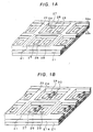
- Step 1 see FIG. 1A
- the large substrate 21 is formed of an insulating material such as ceramic or glass epoxy and has a thickness of 100-500 ⁇ m.
- the substrate 21 has a first main surface 22a comprising the top surface and a second main surface 22b comprising the bottom surface.
- a lattice-like side portion 23 is formed of rail-like members having a height of 0.4 mm and a width of 0.5 mm and is disposed around the outer circumference of each chip mounting area on the substrate 21, forming depressions 24 in the center of the mounting area.
- a second substrate 21a is formed with a plurality of holes corresponding to the positions of the depressions 24.
- the depressions 24 are formed by affixing this second substrate 21a to the substrate 21, wherein both substrates have the thickness described above.
- the substrate 21 and second substrate 21a can also be provided as one integrally formed part.
- Each of the depressions 24 has dimensions of approximately 0.8 x 0.6 mm.
- the depressions 24 are arranged on the substrate 21 at regular intervals both longitudinally and latitudinally.
- a plurality of groups each including an island 26 and electrodes 27 and 28 are formed of conductive patterns on the first main surface 22a using such material as gold plating, wherein one group is disposed in each depression 24.
- the island 26 penetrates the center of the depression 24 in the shape of a belt separating the electrodes 27 and 28.
- Each depression 24 and a portion of the side portion 23 surrounding the depression 24 form an chip mounting section 41.
- Step 2 see FIG. 1B
- a semiconductor chip 29 is die-bonded to the island 26 in each depression 24.
- Bonding wires 30 are wire-bonded to the semiconductor chip 29 and each of the electrodes 27 and 28.
- the height of the loop formed by the bonding wires 30 should be less than the height of the side portion 23.
- Step 3 see FIG. 2A
- One plate-shaped cover member 36 is prepared.
- the cover member 36 has a thickness of approximately 0.15-0.25 mm and is formed of a ceramic or an organic insulating material.
- the cover member 36 is bonded to the top of the side portion 23 to span the entire plurality of chip mounting sections 41 and hermetically seal each of the depressions 24.
- An epoxy adhesive or the like is used to bond the cover member 36 to the side portion 23. With this construction the semiconductor chip 29 and bonding wires 30 are contained within a completely airtight hollow space.
- Step 4 see FIG. 2B
- Each of the chip mounting sections 41 is separated by cutting along the guide marks on the surface of the substrate 21 to obtain individual devices.
- a dicing plate 42 is used to separate the chip mounting sections 41. The process is conducted by fixing a dicing sheet to the bottom surface of the substrate 21 (second main surface 22b) and cutting through the substrate 21 and cover member 36 along longitudinal and latitudinal dicing lines 43 using the dicing plate 42.
- the dicing lines 43 are positioned along the center of the side portion 23. It is also possible to attach a dicing sheet to the cover member 36.
- FIGS. 3A and 3B shows the manufacturing method for a semiconductor device according to a second embodiment of the present invention.
- the side portion 23 is integrally formed with the cover member 36.
- Step 1 see FIG. 3A
- the large substrate 21 is formed of an insulating material such as ceramic or glass epoxy and has a thickness of 0.1-0.5 mm.
- the substrate 21 has a first main surface 22a comprising the top surface and a second main surface 22b comprising the bottom surface.
- a plurality of groups comprising an island 26 and electrodes 27 and 28 are formed on the first main surface 22a using a conductive pattern formed of such material as gold plating.
- the area surrounding the island 26 and the electrodes 27 and 28 is the chip mounting section 41. Chip mounting sections 41 are arranged at equal intervals from each other longitudinally and latitudinally.
- the island 26 penetrates the center of the depression 24 in the shape of a belt separating the electrodes 27 and 28.
- a semiconductor chip 29 is die-bonded on the island 26 in each chip mounting section 41 and bonding wires 30 are wire-bonded to the semiconductor chip 29 and each of the electrodes 27 and 28.
- Step 2 see FIG. 3B
- a cover member 36 is prepared.
- the cover member 36 has a thickness of approximately of 0.1-0.3 mm and is formed of ceramic or an organic insulating material.
- the lattice-shaped side portion 23 having a height of approximately 0.1-0.2 mm and a width of 0.2-0.5 mm is integrally formed with the cover member 36 to form a plurality of depressions 24.
- the depressions 24 face the first main surface 22a and surround each of the chip mounting sections 41.
- the depressions 24 are approximately 0.8 x 0.6 mm in size and are arranged at equal intervals from each other longitudinally and latitudinally.
- the cover member 36 is bonded to the substrate 21 such that each of the chip mounting sections 41 is contained within a depression 24.
- An epoxy adhesive or the like is used to bond the cover member 36 to the substrate 21.
- the semiconductor chip 29 and bonding wires 30 are contained within a completely airtight hollow space. Since the die-bonding and wire-bonding can be performed on the substrate 21 in the present embodiment, there is no need for an adsorption collet or bonding tool to contact the side portion 23. Accordingly, the depressions 24 can be constructed with smaller dimensions.
- Step 3 (not shown)
- each of the chip mounting sections 41 is separated by cutting along the guide marks to obtain individual devices (not shown).
- a dicing plate 42 is used to separate the chip mounting sections 41.
- the process is conducted by fixing a dicing sheet to the bottom surface of the substrate 21 (second main surface 22b) and cutting through the substrate 21 and cover member 36 along longitudinal and latitudinal dicing lines 43 using the dicing plate 42.
- the dicing lines 43 are positioned along the center of the side portion 23. It is also possible to attach a bonding sheet to the cover member 36.
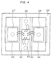
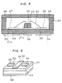
- FIGS. 4 and 5 are plan and cross-sectional views showing a high-frequency semiconductor device manufactured according to the first embodiment.
- FIG. 6 is a perspective view from the bottom side of the device.
- a substrate 21a separated from the substrate 21 has a rectangular shape with dimensions approximately 1.5 x 2.5 mm.
- the high-frequency semiconductor chip 29 die-bonded to the island 26 of the substrate 21a is, for example, a Schottky barrier diode, MMIC, GaAsFET, or the like.
- the electrode pads formed on the surface of the semiconductor chip 29 are connected to the electrodes 27 and 28 by the bonding wires 30. Since the island 26 is formed in a belt shape between the electrodes 27 and 28, an FET using the island 26 as a source achieves a reduced stray capacity between the gate electrode 27 and the drain electrode 28.
- External connectors 32, 33, and 34 are formed on the second main surface 22b of the substrate 21a by conductive patterns formed of gold plating or the like.
- the external connectors 32, 33, and 34 approximate the pattern of the island 26, and electrodes 27 and 28.
- Via holes 35 corresponding to each of the external connectors 32, 33, and 34 penetrate the substrate 21a from the first main surface 22a to the second main surface 22b.
- the via holes 35 are filled with a conducting material such as tungsten, silver, copper, or the like, electrically connecting the island 26 to the external connector 33, the electrode 27 to the external connector 32, and the electrode 28 to the external connector 34.
- the edges of the external connectors 32, 33, and 34 are set back approximately 0.1-0.2 mm from the edges of the substrate 21. It is desirable for the bonding wires 30 to be connected to the electrodes 27 and 28 directly over the via holes 35.
- the external connectors 32, 33, and 34 are preformed on the large substrate 21.
- the side portion 23 After being cut in the dicing process, the side portion 23 surrounds the semiconductor chip 29 and a cover member 36 seals the semiconductor chip 29 in an airtight hollow space.
- An adhesive 37 is used to bond the side portions 23 to the first main surface 22a and the side portions 23 to the cover member 36.
- the semiconductor chip 29 and the fine metallic wires 30 are contained within the airtight hollow space formed by the depression 24. Cutting the substrate 21, side portions 23, and cover member 36 in the dicing process forms a flat surface on the outer side faces of the same.
- the electronic part described above is mounted such that the external connectors 32, 33, and 34 are bonded directly opposite the electrode patterns on the mounting substrate. With this construction, the electrode 32 functions as a shield between the connectors 33 and 34.
- the semiconductor device is manufactured by cutting an encapsulating package suitable for a high-frequency chip from a common substrate wafer. This procedure simplifies the manufacturing process and reduces the external size of the device, thereby reducing production costs.
- the island can readily function as a shield between the electrodes, serving as the gate and drain, when mounting an FET chip or the like.
Landscapes
- Wire Bonding (AREA)
- Light Receiving Elements (AREA)
- Structures Or Materials For Encapsulating Or Coating Semiconductor Devices Or Solid State Devices (AREA)
- Surface Acoustic Wave Elements And Circuit Networks Thereof (AREA)
- Pressure Sensors (AREA)
- Solid State Image Pick-Up Elements (AREA)
Abstract
Description
Claims (4)
- A manufacturing method for a semiconductor device, comprising:preparing a common substrate having opposing first and second main surfaces and a plurality of mounting sections formed in the first main surface, each of the mounting sections being provided with an island section for mounting a semiconductor chip and electrode sections disposed on opposing sides of the island section for connecting to the electrodes of the semiconductor chip;fixing a semiconductor chip onto each of the mounting sections;fixing a cover over the plurality of mounting sections for hermetically sealing each of the semiconductor chips, which is mounted in a hollow space formed thereby; andseparating the mounting sections, each retaining their corresponding portions of cover and substrate to produce a semiconductor device having a hermetically sealed semiconductor chip.
- A manufacturing method for a semiconductor device as claimed in claim 1, wherein the island sections extend across the approximate center of the mounting sections and are disposed between the electrode sections.
- A manufacturing method for a semiconductor device as claimed in claim 1, wherein external connecting electrodes are formed on the second main surface of the substrate and are disposed in correspondence with the island sections and the electrode sections.
- A manufacturing method for a semiconductor device as claimed in claim 1, wherein the step for separating the mounting sections is a dicing process.
Applications Claiming Priority (2)
| Application Number | Priority Date | Filing Date | Title |
|---|---|---|---|
| JP22341099 | 1999-08-06 | ||
| JP22341099A JP3462806B2 (en) | 1999-08-06 | 1999-08-06 | Semiconductor device and manufacturing method thereof |
Publications (2)
| Publication Number | Publication Date |
|---|---|
| EP1075020A2 true EP1075020A2 (en) | 2001-02-07 |
| EP1075020A3 EP1075020A3 (en) | 2005-12-14 |
Family
ID=16797719
Family Applications (1)
| Application Number | Title | Priority Date | Filing Date |
|---|---|---|---|
| EP20000202741 Withdrawn EP1075020A3 (en) | 1999-08-06 | 2000-08-02 | Method for packaging semiconductor device |
Country Status (5)
| Country | Link |
|---|---|
| US (1) | US6521482B1 (en) |
| EP (1) | EP1075020A3 (en) |
| JP (1) | JP3462806B2 (en) |
| KR (1) | KR100347506B1 (en) |
| TW (1) | TW449889B (en) |
Families Citing this family (10)
| Publication number | Priority date | Publication date | Assignee | Title |
|---|---|---|---|---|
| US8623709B1 (en) | 2000-11-28 | 2014-01-07 | Knowles Electronics, Llc | Methods of manufacture of top port surface mount silicon condenser microphone packages |
| US7434305B2 (en) | 2000-11-28 | 2008-10-14 | Knowles Electronics, Llc. | Method of manufacturing a microphone |
| US7566587B2 (en) * | 2001-12-03 | 2009-07-28 | Azimuth Industrial Co., Inc. | Method and apparatus for packaging electronic components |
| JP3881888B2 (en) * | 2001-12-27 | 2007-02-14 | セイコーエプソン株式会社 | Optical device manufacturing method |
| US6747341B2 (en) * | 2002-06-27 | 2004-06-08 | Semiconductor Components Industries, L.L.C. | Integrated circuit and laminated leadframe package |
| US8303756B2 (en) * | 2004-12-07 | 2012-11-06 | Lg Display Co., Ltd. | Method for bonding a glass cap and mask for curing sealant |
| JP5270349B2 (en) * | 2006-08-25 | 2013-08-21 | セミコンダクター・コンポーネンツ・インダストリーズ・リミテッド・ライアビリティ・カンパニー | Semiconductor device and manufacturing method thereof |
| US9374643B2 (en) | 2011-11-04 | 2016-06-21 | Knowles Electronics, Llc | Embedded dielectric as a barrier in an acoustic device and method of manufacture |
| US9078063B2 (en) | 2012-08-10 | 2015-07-07 | Knowles Electronics, Llc | Microphone assembly with barrier to prevent contaminant infiltration |
| US9794661B2 (en) | 2015-08-07 | 2017-10-17 | Knowles Electronics, Llc | Ingress protection for reducing particle infiltration into acoustic chamber of a MEMS microphone package |
Family Cites Families (5)
| Publication number | Priority date | Publication date | Assignee | Title |
|---|---|---|---|---|
| US5976912A (en) * | 1994-03-18 | 1999-11-02 | Hitachi Chemical Company, Ltd. | Fabrication process of semiconductor package and semiconductor package |
| JP2679681B2 (en) * | 1995-04-28 | 1997-11-19 | 日本電気株式会社 | Semiconductor device, package for semiconductor device, and manufacturing method thereof |
| JP2760339B2 (en) * | 1996-03-05 | 1998-05-28 | 日本電気株式会社 | Lead frame deburring method and lead frame deburring device |
| JP3652488B2 (en) * | 1997-12-18 | 2005-05-25 | Tdk株式会社 | Manufacturing method of resin package |
| US5923958A (en) * | 1998-05-28 | 1999-07-13 | Pan Pacific Semiconductor Co., Ltd. | Method for semiconductor chip packaging |
-
1999
- 1999-08-06 JP JP22341099A patent/JP3462806B2/en not_active Expired - Fee Related
-
2000
- 2000-07-10 TW TW89113677A patent/TW449889B/en not_active IP Right Cessation
- 2000-08-02 EP EP20000202741 patent/EP1075020A3/en not_active Withdrawn
- 2000-08-03 US US09/632,170 patent/US6521482B1/en not_active Expired - Lifetime
- 2000-08-05 KR KR1020000045420A patent/KR100347506B1/en not_active Expired - Fee Related
Also Published As
| Publication number | Publication date |
|---|---|
| JP3462806B2 (en) | 2003-11-05 |
| JP2001053180A (en) | 2001-02-23 |
| EP1075020A3 (en) | 2005-12-14 |
| TW449889B (en) | 2001-08-11 |
| KR20010070016A (en) | 2001-07-25 |
| KR100347506B1 (en) | 2002-08-03 |
| US6521482B1 (en) | 2003-02-18 |
Similar Documents
| Publication | Publication Date | Title |
|---|---|---|
| US7008824B2 (en) | Method of fabricating mounted multiple semiconductor dies in a package | |
| US6297547B1 (en) | Mounting multiple semiconductor dies in a package | |
| US5638596A (en) | Method of employing multi-layer tab tape in semiconductor device assembly by selecting, breaking, downwardly bending and bonding tab tape trace free ends to a ground or power plane | |
| JP3420153B2 (en) | Semiconductor device and manufacturing method thereof | |
| KR100339044B1 (en) | ball grid array semiconductor package and method for making the same | |
| US7338838B2 (en) | Resin-encapsulation semiconductor device and method for fabricating the same | |
| US6861760B2 (en) | Semiconductor device with stacked-semiconductor chips and support plate | |
| JPH11312706A (en) | Resin-sealed semiconductor device, method of manufacturing the same, and lead frame | |
| US6815808B2 (en) | Hollow airtight semiconductor device package | |
| US20010042898A1 (en) | Electronic device and method for manufacturing the same | |
| US6521482B1 (en) | Manufacturing method for a semiconductor device | |
| US7161232B1 (en) | Apparatus and method for miniature semiconductor packages | |
| US6774479B2 (en) | Electronic device having a semiconductor chip on a semiconductor chip connection plate and a method for producing the electronic device | |
| KR20030027413A (en) | Multi chip package having spacer that is inserted between chips and manufacturing method thereof | |
| US5808872A (en) | Semiconductor package and method of mounting the same on circuit board | |
| JPH09307051A (en) | Resin-sealed semiconductor device and method of manufacturing the same | |
| JP3269025B2 (en) | Semiconductor device and manufacturing method thereof | |
| US7226813B2 (en) | Semiconductor package | |
| KR100387171B1 (en) | Method of producing semiconductor device and configuration thereof | |
| US20210384151A1 (en) | Semiconductor devices and methods of manufacturing semiconductor devices | |
| US20040000674A1 (en) | Optically coupled semiconductor device and method for manufacturing the same | |
| JP2574510B2 (en) | High frequency semiconductor device | |
| JPS6352461A (en) | Semiconductor device | |
| JP3203228B2 (en) | Semiconductor device and manufacturing method thereof | |
| JP3819607B2 (en) | Semiconductor device and manufacturing method thereof |
Legal Events
| Date | Code | Title | Description |
|---|---|---|---|
| PUAI | Public reference made under article 153(3) epc to a published international application that has entered the european phase |
Free format text: ORIGINAL CODE: 0009012 |
|
| AK | Designated contracting states |
Kind code of ref document: A2 Designated state(s): AT BE CH CY DE DK ES FI FR GB GR IE IT LI LU MC NL PT SE |
|
| AX | Request for extension of the european patent |
Free format text: AL;LT;LV;MK;RO;SI |
|
| PUAL | Search report despatched |
Free format text: ORIGINAL CODE: 0009013 |
|
| AK | Designated contracting states |
Kind code of ref document: A3 Designated state(s): AT BE CH CY DE DK ES FI FR GB GR IE IT LI LU MC NL PT SE |
|
| AX | Request for extension of the european patent |
Extension state: AL LT LV MK RO SI |
|
| 17P | Request for examination filed |
Effective date: 20060502 |
|
| AKX | Designation fees paid |
Designated state(s): DE FR GB |
|
| 17Q | First examination report despatched |
Effective date: 20060904 |
|
| STAA | Information on the status of an ep patent application or granted ep patent |
Free format text: STATUS: THE APPLICATION IS DEEMED TO BE WITHDRAWN |
|
| 18D | Application deemed to be withdrawn |
Effective date: 20070116 |