EP1074864A2 - Method of fabricating planar optical waveguide devices - Google Patents
Method of fabricating planar optical waveguide devices Download PDFInfo
- Publication number
- EP1074864A2 EP1074864A2 EP00202766A EP00202766A EP1074864A2 EP 1074864 A2 EP1074864 A2 EP 1074864A2 EP 00202766 A EP00202766 A EP 00202766A EP 00202766 A EP00202766 A EP 00202766A EP 1074864 A2 EP1074864 A2 EP 1074864A2
- Authority
- EP
- European Patent Office
- Prior art keywords
- clad layer
- layer
- core
- lower clad
- optical waveguide
- Prior art date
- Legal status (The legal status is an assumption and is not a legal conclusion. Google has not performed a legal analysis and makes no representation as to the accuracy of the status listed.)
- Withdrawn
Links
- 230000003287 optical effect Effects 0.000 title claims abstract description 51
- 238000004519 manufacturing process Methods 0.000 title abstract description 18
- 239000010410 layer Substances 0.000 claims abstract description 182
- 238000000034 method Methods 0.000 claims abstract description 121
- 230000008569 process Effects 0.000 claims abstract description 95
- 239000000758 substrate Substances 0.000 claims abstract description 51
- 238000001513 hot isostatic pressing Methods 0.000 claims abstract description 37
- 230000007062 hydrolysis Effects 0.000 claims abstract description 10
- 238000006460 hydrolysis reaction Methods 0.000 claims abstract description 10
- 239000012792 core layer Substances 0.000 claims description 76
- 239000011521 glass Substances 0.000 claims description 12
- 238000000059 patterning Methods 0.000 claims description 4
- 238000005137 deposition process Methods 0.000 claims 6
- 239000002344 surface layer Substances 0.000 claims 1
- 239000011241 protective layer Substances 0.000 abstract description 8
- 230000004888 barrier function Effects 0.000 abstract description 5
- 238000003825 pressing Methods 0.000 abstract 1
- 239000011162 core material Substances 0.000 description 54
- VYPSYNLAJGMNEJ-UHFFFAOYSA-N Silicium dioxide Chemical compound O=[Si]=O VYPSYNLAJGMNEJ-UHFFFAOYSA-N 0.000 description 34
- 239000002019 doping agent Substances 0.000 description 19
- 238000005229 chemical vapour deposition Methods 0.000 description 17
- 229910052681 coesite Inorganic materials 0.000 description 13
- 229910052906 cristobalite Inorganic materials 0.000 description 13
- 239000000377 silicon dioxide Substances 0.000 description 13
- 229910052682 stishovite Inorganic materials 0.000 description 13
- 229910052905 tridymite Inorganic materials 0.000 description 13
- 239000010936 titanium Substances 0.000 description 12
- 238000001020 plasma etching Methods 0.000 description 10
- 239000000463 material Substances 0.000 description 8
- 238000005530 etching Methods 0.000 description 7
- 239000007789 gas Substances 0.000 description 7
- 238000010438 heat treatment Methods 0.000 description 7
- 229920002120 photoresistant polymer Polymers 0.000 description 7
- XKRFYHLGVUSROY-UHFFFAOYSA-N Argon Chemical compound [Ar] XKRFYHLGVUSROY-UHFFFAOYSA-N 0.000 description 6
- KRHYYFGTRYWZRS-UHFFFAOYSA-M Fluoride anion Chemical compound [F-] KRHYYFGTRYWZRS-UHFFFAOYSA-M 0.000 description 6
- OAICVXFJPJFONN-UHFFFAOYSA-N Phosphorus Chemical compound [P] OAICVXFJPJFONN-UHFFFAOYSA-N 0.000 description 6
- RTAQQCXQSZGOHL-UHFFFAOYSA-N Titanium Chemical compound [Ti] RTAQQCXQSZGOHL-UHFFFAOYSA-N 0.000 description 6
- XAGFODPZIPBFFR-UHFFFAOYSA-N aluminium Chemical compound [Al] XAGFODPZIPBFFR-UHFFFAOYSA-N 0.000 description 6
- 229910052782 aluminium Inorganic materials 0.000 description 6
- 238000002474 experimental method Methods 0.000 description 6
- 229910052732 germanium Inorganic materials 0.000 description 6
- GNPVGFCGXDBREM-UHFFFAOYSA-N germanium atom Chemical compound [Ge] GNPVGFCGXDBREM-UHFFFAOYSA-N 0.000 description 6
- 229910052698 phosphorus Inorganic materials 0.000 description 6
- 239000011574 phosphorus Substances 0.000 description 6
- 229910052719 titanium Inorganic materials 0.000 description 6
- ZOXJGFHDIHLPTG-UHFFFAOYSA-N Boron Chemical compound [B] ZOXJGFHDIHLPTG-UHFFFAOYSA-N 0.000 description 5
- 229910052796 boron Inorganic materials 0.000 description 5
- 239000000919 ceramic Substances 0.000 description 5
- 239000000843 powder Substances 0.000 description 5
- 239000004065 semiconductor Substances 0.000 description 5
- 238000005240 physical vapour deposition Methods 0.000 description 4
- 229910052786 argon Inorganic materials 0.000 description 3
- 238000003486 chemical etching Methods 0.000 description 3
- 238000006243 chemical reaction Methods 0.000 description 3
- 238000004891 communication Methods 0.000 description 3
- 230000008021 deposition Effects 0.000 description 3
- 238000009826 distribution Methods 0.000 description 3
- 239000000835 fiber Substances 0.000 description 3
- 238000005498 polishing Methods 0.000 description 3
- 238000000151 deposition Methods 0.000 description 2
- 230000008030 elimination Effects 0.000 description 2
- 238000003379 elimination reaction Methods 0.000 description 2
- 239000013307 optical fiber Substances 0.000 description 2
- 238000005268 plasma chemical vapour deposition Methods 0.000 description 2
- 238000012360 testing method Methods 0.000 description 2
- UFHFLCQGNIYNRP-UHFFFAOYSA-N Hydrogen Chemical compound [H][H] UFHFLCQGNIYNRP-UHFFFAOYSA-N 0.000 description 1
- 230000004075 alteration Effects 0.000 description 1
- QVGXLLKOCUKJST-UHFFFAOYSA-N atomic oxygen Chemical compound [O] QVGXLLKOCUKJST-UHFFFAOYSA-N 0.000 description 1
- 230000009286 beneficial effect Effects 0.000 description 1
- 230000005540 biological transmission Effects 0.000 description 1
- 230000008859 change Effects 0.000 description 1
- 238000005234 chemical deposition Methods 0.000 description 1
- 230000002950 deficient Effects 0.000 description 1
- 239000001257 hydrogen Substances 0.000 description 1
- 229910052739 hydrogen Inorganic materials 0.000 description 1
- 239000011261 inert gas Substances 0.000 description 1
- 238000007733 ion plating Methods 0.000 description 1
- 239000000203 mixture Substances 0.000 description 1
- 238000012986 modification Methods 0.000 description 1
- 230000004048 modification Effects 0.000 description 1
- 239000001301 oxygen Substances 0.000 description 1
- 229910052760 oxygen Inorganic materials 0.000 description 1
- 239000012495 reaction gas Substances 0.000 description 1
- 238000005245 sintering Methods 0.000 description 1
- 238000004544 sputter deposition Methods 0.000 description 1
- 238000007740 vapor deposition Methods 0.000 description 1
Images


Classifications
-
- G—PHYSICS
- G02—OPTICS
- G02B—OPTICAL ELEMENTS, SYSTEMS OR APPARATUS
- G02B6/00—Light guides; Structural details of arrangements comprising light guides and other optical elements, e.g. couplings
- G02B6/10—Light guides; Structural details of arrangements comprising light guides and other optical elements, e.g. couplings of the optical waveguide type
- G02B6/12—Light guides; Structural details of arrangements comprising light guides and other optical elements, e.g. couplings of the optical waveguide type of the integrated circuit kind
- G02B6/13—Integrated optical circuits characterised by the manufacturing method
- G02B6/132—Integrated optical circuits characterised by the manufacturing method by deposition of thin films
-
- G—PHYSICS
- G02—OPTICS
- G02B—OPTICAL ELEMENTS, SYSTEMS OR APPARATUS
- G02B6/00—Light guides; Structural details of arrangements comprising light guides and other optical elements, e.g. couplings
- G02B6/10—Light guides; Structural details of arrangements comprising light guides and other optical elements, e.g. couplings of the optical waveguide type
- G02B6/12—Light guides; Structural details of arrangements comprising light guides and other optical elements, e.g. couplings of the optical waveguide type of the integrated circuit kind
- G02B2006/12035—Materials
- G02B2006/12038—Glass (SiO2 based materials)
-
- G—PHYSICS
- G02—OPTICS
- G02B—OPTICAL ELEMENTS, SYSTEMS OR APPARATUS
- G02B6/00—Light guides; Structural details of arrangements comprising light guides and other optical elements, e.g. couplings
- G02B6/10—Light guides; Structural details of arrangements comprising light guides and other optical elements, e.g. couplings of the optical waveguide type
- G02B6/12—Light guides; Structural details of arrangements comprising light guides and other optical elements, e.g. couplings of the optical waveguide type of the integrated circuit kind
- G02B2006/12133—Functions
- G02B2006/12147—Coupler
-
- G—PHYSICS
- G02—OPTICS
- G02B—OPTICAL ELEMENTS, SYSTEMS OR APPARATUS
- G02B6/00—Light guides; Structural details of arrangements comprising light guides and other optical elements, e.g. couplings
- G02B6/10—Light guides; Structural details of arrangements comprising light guides and other optical elements, e.g. couplings of the optical waveguide type
- G02B6/12—Light guides; Structural details of arrangements comprising light guides and other optical elements, e.g. couplings of the optical waveguide type of the integrated circuit kind
- G02B2006/12133—Functions
- G02B2006/1215—Splitter
-
- G—PHYSICS
- G02—OPTICS
- G02B—OPTICAL ELEMENTS, SYSTEMS OR APPARATUS
- G02B6/00—Light guides; Structural details of arrangements comprising light guides and other optical elements, e.g. couplings
- G02B6/10—Light guides; Structural details of arrangements comprising light guides and other optical elements, e.g. couplings of the optical waveguide type
- G02B6/12—Light guides; Structural details of arrangements comprising light guides and other optical elements, e.g. couplings of the optical waveguide type of the integrated circuit kind
- G02B2006/12166—Manufacturing methods
- G02B2006/12176—Etching
Definitions
- the present invention relates to planar optical waveguide devices, and in particular to a method for fabricating planar optical waveguide devices which are, not exclusively, suited for use in the field of optical communication.
- Japanese patent laid open publications Nos. 61-210304 and 1-189614 disclose planar optical waveguide devices having an embedded structure. The various layers are formed either by CVD or deposition of glass powder followed by sintering (FHD: flame hydrolysis deposition).
- Japanese patent laid open publication No. 61-210304 proposes to form a recess in a substrate to form a core therein. To achieve a desired circular cross section, the recess having a rectangular cross section is fire polished so as to have a more circular cross section as illustrated in Figure 1 of this prior patent publication.
- Such a waveguide device can be fabricated as summarized in the following.
- a substrate or a buffer layer serving as a lower clad layer is prepared, and a core layer is formed on the lower clad layer.
- the core layer is appropriately patterned into core segments of a desired configuration typically by reactive ion etching (RIE).
- RIE reactive ion etching
- an upper clad layer is placed on both the core and the lower clad layer.
- the obtained assembly is then cut into a desired size and configuration, and the input and output ends of the assembly is polished into optical planes.
- These layers are typically made of SiO 2 , and a desired refractive index distribution can be achieved by adding suitable dopants to the appropriate layers.
- a low-temperature film-forming process such as CVD, plasma CVD, PVD, and vacuum PVD is advantageous in controlling the thickness of each layer, and evenly distributing dopants in each layer.
- the upper clad layer may fail to fill the gaps between adjacent core segments or the material for the core may fail to fill the recess in the lower clad layer, and voids may develop in the upper clad layer or the core. Such voids are known to reduce the transmission efficiency of the device due to the scattering of the signal light, and are desired to be eliminated.
- the upper clad layer may be placed on a planar surface, and creation of voids in the upper clad layer can be avoided.
- voids tend to be produced in the core by the material of the core failing to fill the recess completely.
- FHD involves a higher temperature, and allows the material to fill gaps or recesses more freely, in particular by properly selecting the softening point of the selected glass material.
- controlling the softening point requires addition of dopants which are also known to change the refractive index of the material. Therefore, it is difficult to adjust the amount and selection of dopants which would result in a desired softening point and refractive index at the same time.
- a desired softening point may not be achieved, and voids may be created in the upper clad layer or the core.
- the inventors proposed the use of the hot isostatic pressing (HIP) process for removing voids that may be created in the upper clad layer in Japanese patent laid open publication No. 11-125727.
- HIP hot isostatic pressing
- a primary object of the present invention is to provide a method for fabricating planar optical waveguide devices which can eliminate voids that may develop in the core and/or upper clad layer of an optical waveguide device.
- a second object of the present invention is to provide a method for fabricating planar optical waveguide devices which can minimize the possibility of defective products, and can thereby reduce the fabrication cost of each unit.
- a third object of the present invention is to provide a method for fabricating planar optical waveguide devices which can fabricate durable devices through elimination of residual stresses in each layer of the device.
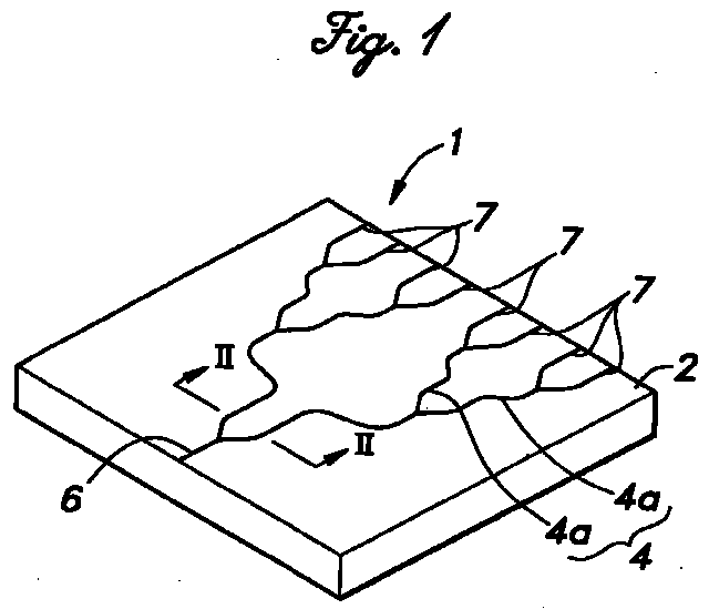
- FIG. 1 is a perspective view of a planar optical waveguide device embodying the present invention.
- This device 1 has an embedded waveguide structure, and includes a core 4 having a branched configuration and consisting of a number of core segments 4a, to split optical signals in the field of optical communication, for instance.
- an input signal is applied to an input end 6 of the core 4 defined on one side of the device, and an output signal is produced from each one of a plurality of output ends 7 of the core 4 defined on the opposite side of the device.
- the core 4 is formed on a substrate 2 serving as a lower clad layer, and an upper clad layer 5 is formed over both the core 4 and the otherwise exposed surface of the substrate 2.
- the substrate 2 consists of silica glass in this case.
- the core 4 has a 8 by 8 ⁇ m square cross section, and has a slightly higher refractive index than the substrate 2 and the upper clad layer 5, to conduct signal light therein according the well-known principle of fiber optics.
- the upper clad layer 5 typically has a thickness of 25 ⁇ m.
- Phosphorus (P), titanium (Ti), germanium (Ge) and aluminum (Al) are known to raise the refractive index while boron (B) and fluoride (F) are known to lower the refractive index. By using one of them or two or more of them in combination, a desired refractive index can be achieved.
- the refractive index of the core layer 4' is matched with or made to agree with that of the core of the optical fiber that is to be connected to the optical waveguide device 1.
- the core layer 4' is doped, and the substrate 2 and the upper clad layer 5 are not doped. If necessary, the substrate 2 and the upper clad layer 5 may also be doped so that the refractive index of the substrate and the upper clad layer may be made adequately lower than that of the core layer 4' while the refractive index of the core layer 4' is matched with that of the core of the optical fiber.
- Figure 4 shows a CVD system for conducting a CVD process.
- the substrates 2 are held by a holder 20 inside a reaction chamber 10 and reaction gases are passed through the reaction chamber 20 while the substrates 2 are heated by a heater 30 so as to form the core layer 4' on the surface of each substrate 2.
- the process for forming the core layer 4' is not limited to the CVD process, but may also consist of a plasma CVD, physical vapor deposition (PVD), vacuum vapor deposition, sputtering, ion plating and other lower-temperature film-forming processes.
- a preliminary heating process may be conducted under a pressure or at the atmoshperic pressure.
- the temperature involved in this heating process may be higher than that for the film-forming step for the core layer 4' but lower than that for the subsequent heating/pressurizing step (which is described hereinafter).
- a prescribed waveguide pattern is defined on the surface of the core layer 4' with photoresist, and the core 4 having a desired waveguide pattern is formed by etching such as RIE (reactive ion etching) ( Figure 3b).
- the upper clad layer 5 essentially made of SiO 2 having a relatively low refractive index is formed by a similar low-temperature film-forming process (Figure 3c).
- Figure 3c The upper clad layer 5 essentially made of SiO 2 having a relatively low refractive index is formed by a similar low-temperature film-forming process.
- voids 8 tend to develop in the gaps between adjacent segments of the core 4 by the material of the upper clad layer 5 failing to entirely fill into the gaps, particularly when the core segments are disposed closely next to each other.
- HIP hot isostatic pressing
- the heat and pressure also help remove internal stresses that may have developed in the substrate 2 and the layers 4 and 5 deposited thereon during the film-forming steps ( Figure 3d).
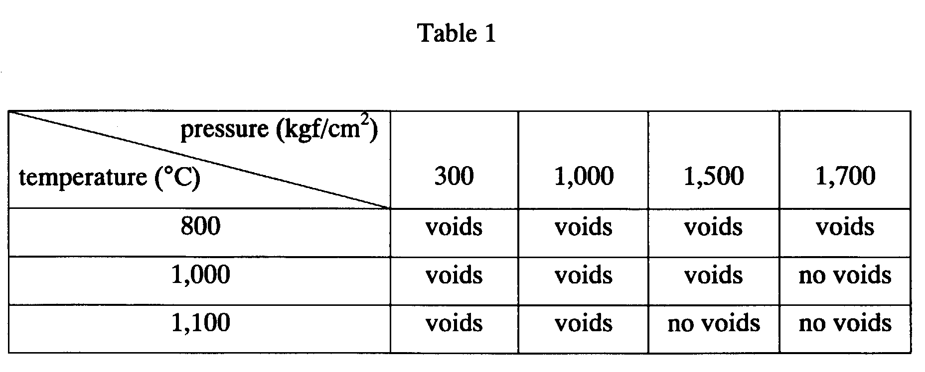
- the HIP process typically involves the pressurization of the device at 1,500 kgf/cm 2 by using inert gas such as argon (Ar) at a temperature of 1,200 °C over a time period of about two hours. Because the pressure is uniformly applied to the device, the shape of the device would not be changed.
- the substrate 2 is cut into the desired size and shape with a dicing machine, and the end surfaces for the input and outer ends 6 and 7 are polished into optical planes.
- Figure 5 shows a second embodiment of the present invention.
- a buffer layer 3 serving as a lower clad layer is formed on a substrate 2 consisting of a wafer of silica glass, ceramics or semiconductor, and a core 4 is formed on the buffer layer 3.
- An upper clad layer 5 is then formed over both the buffer layer 3 and the core 4.
- the buffer layer 3 made of SiO 2 is formed on the surface of the substrate 2 with a low-temperature film-forming process such as CVD, similarly as the first embodiment ( Figure 6a).
- a core layer 4' made of SiO 2 is formed on the surface of the buffer layer 3 with a low-temperature film-forming process such as CVD, similarly as the first embodiment ( Figure 6b).
- a dopant is added to the core layer 4' to control the regractive index of the core layer 4'. If desired, at this stage, a preliminary heating process may be conducted either at a high pressure or atmospheric pressure.
- a waveguide pattern is formed on the surface of the core layer 4' by using photoresist, and a waveguide core 4 of a prescribed pattern is them formed by etching the core layer 4' by RIE, for instance ( Figure 6c).
- An upper clad layer 5 having a relatively low refractive index is formed over the core 4 and the buffer layer 3 by CVD ( Figure 6d). If necessary, a dopant may be added to both the buffer layer 3 and the upper clad layer 5 to lower the refractive index of these layers.
- the device 1 is then subjected to the HIP process with the surface of the upper clad layer 5 exposed so that the voids 8 may be reduced to a tolerable level or totally eliminated, and the internal stresses that may have developed in the substrate 2 and the layers 3,4 and 5 formed thereon during the film-forming steps ( Figure 6e).
- the produced assembly is then cut into the desired size and shape, and the input and output ends of the device are polished into optical planes.
- Figures 7a to 7e show the fabrication process for a third embodiment of the present invention.
- a photoresist layer in a prescribed waveguide pattern is placed on the surface of a substrate 12 which may be made of silica glass, and an etching process such as RIE is conducted on the substrate 12 to form a recess 12a in the prescribed pattern ( Figure 7a).
- a core layer 14' is formed on the surface of the substrate 12 by a low-temperature film-forming process such as CVD ( Figure 7b). At this point, a dopant is added to the core layer 14' to raise the refractive index of the core layer 14' by 0.2 to 0.8% from that of the substrate 12.
- the core layer 14', in particular the part of the core layer which is inside the recess 12a may contain voids 18 therein by the core material failing to flow into and fill the recess 12a.
- the produced assembly is subjected to the HIP process with the surface of the core layer 14' exposed so as to reduce or eliminate the voids 18 and remove the internal stresses that may have developed in the substrate 12 and the core layer 14' during the preceding film-forming step ( Figure 7c). Then, the surface of the assembly is removed until the surface of the substrate 12 is exposed either by physical polishing or chemical etching ( Figure 7d). This results in a core 14 formed in the recess 12a of the substrate 12, and the core 14 and the substrate 12 jointly define a planar surface.
- An upper clad layer 15 essentially made of SiO 2 and having a relatively lower refractive index is formed on the planar surface jointly defined by the core 14 and the substrate 12 by a low-temperature film-forming process such as CVD ( Figure 7e).
- the assembly is then cut into the desired size and shape, and the input and output ends of the device are polished into optical planes.
- Figures 8a to 8f show the fabrication process for a fourth embodiment of the present invention.
- a buffer layer 13 serving as a lower clad layer is formed on the surface of a substrate 12 which may be made of a wafer of semiconductor, silica glass or ceramics ( Figure 8a) by a low-temperature film-forming process such as CVD.
- a photoresist layer is placed on the surface of the buffer layer 13 in a prescribed waveguide pattern and an etching process such as RIE is conducted on the buffer layer 13 to form a recess 13a in the prescribed pattern ( Figure 8b).
- a core layer 14' is formed on the surface of the buffer layer 13 by a low-temperature film-forming process such as CVD ( Figure 8c). At this point, a dopant is added to the core layer 14' to raise the refractive index of the core layer 14' by 0.2 to 0.8% from that of the buffer layer 13.
- the core layer 14' in particular the part of the core layer which is inside the recess 13a, may contain voids 18 therein.
- the assembly is subjected to the HIP process with the surface of the core layer 14' exposed so as to reduce or eliminate the voids 18 and remove the internal stresses that may have developed in the substrate 12, the buffer layer 13 and the core layer 14' during the preceding film-forming steps ( Figure 8d). Then, the surface of the assembly is removed until the surface of the buffer layer 13 is exposed either by physical polishing or chemical etching ( Figure 8e). This results in a core 14 formed in the recess 13a of the buffer layer 13, and the core 14 and the buffer layer 13 jointly define a planar surface.
- An upper clad layer 15 essentially made of SiO 2 and having a relatively lower refractive index is formed on the planar surface jointly defined by the core 14 and the buffer layer 13 by a low-temperature film-forming process such as CVD ( Figure 8f).
- the assembly is then cut into the desired size and shape, and the input and output ends of the device are polished into optical planes.
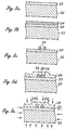
- Figures 9a to 9e show the fabrication process for a fifth embodiment of the present invention.
- a buffer layer 23 is formed on the surface of a substrate 22 which may consist of a wafer made of semiconductor, silica glass or ceramics ( Figure 9a) by the flame hydrolysis deposition (FHD) process.
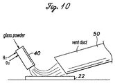
- the FHD process is typically conducted by feeding glass powder into the flame of a torch 40 for burning the mixture of hydrogen and oxygen gases as illustrated in Figure 12.
- the glass powder is heated in the flame, and is deposited on the surface of the substrate as it is hydrolyzed.
- the deposited glass is heated, and forms a film over the surface of the substrate 22.
- a vent duct 50 rapidly vents the gas which is produced from the heating of the glass powder.
- the FHD is not limited to this process using an oxyhydrogen torch, but may also consist of other processes in which glass powder is fed into a flame, and blown onto the surface of the substrate to form a film thereon.
- the buffer layer 23 typically consists of SiO 2 .
- a core layer 24' essentially consisting of SiO 2 is similarly formed by the FHD process on the surface of the buffer layer 23.
- the core layer 24' is appropriately doped by using one or more of the dopants selected from a group consisting of phosphorus (P), titanium (Ti), germanium (Ge), aluminum (Al), Boron (B) and fluoride (F) for the purpose of increasing the refractive index of the core layer 24' by 0.2 to 0.8% over that of the buffer layer 23.
- Phosphorus (P), titanium (Ti), germanium (Ge) and aluminum (Al) are known to raise the refractive index while aoron (B) and fluoride (F) are known to lower the refractive index.
- the refractive index of the core layer 24' is matched with or made to agree with that of the core of the optically fiber that is to be connected to the optical waveguide device.
- the assembly may be subjected to a preliminary heating process at a high pressure or at the atmospheric pressure. Then, a photoresist layer is placed on the surface of the core layer 24' in a prescribed waveguide pattern and an etching process such as the RIE process is conducted on the core layer 24' to form a core 24 in the prescribed pattern ( Figure 9c).
- an upper clad layer 25 essentially made of SiO 2 and having a relatively low refractive index is placed on the surface of the core 24 and the buffer layer 23 by the FHD process ( Figure 9d).
- the refractive index of the upper clad layer 25 is typically identical to that of the buffer layer 23 which is lower than that of the core 24.
- voids 28 tend to develop in the upper clad layer 25 particularly in the regions between adjacent segments of the core 24. This is particularly pronounced when an adequate amount of dopant for lowering the softening point is not added to the upper clad layer 25.
- the assembly is subjected to the HIP process with the surface of the core layer 24' exposed so as to reduce or eliminate the voids 28 and remove the internal stresses that may have developed in the substrate 22, the buffer layer 23, the core 24 and the upper clad layer 25 during the preceding film-forming steps ( Figure 9e).
- the assembly is then cut into the desired size and shape, and the input and output ends of the device are polished into optical planes.
- the temperature and pressure conditions for eliminating voids substantially agreed to those which were observed when the similar experiments were conducted on the device which were based on the low-temperature film-forming process as opposed to the FHD process.
- the conditions may vary depending on the kinds and amounts of dopants that are added to the upper clad layer to control the softening point thereof.
- the pressure and temperature should be selected as low as possible so long as voids can be eliminated to a tolerable level.
- the HIP process can be applied to the device without using any protective layer if any excessive pressure or temperature is not selected for the HIP process.
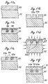
- Figures 11a to 11f show the fabrication process for a sixth embodiment of the present invention.
- a buffer layer 33 serving as a lower clad layer is formed on the surface of a substrate 32, which may consist of a wafer made of semiconductor, silica glass or ceramics ( Figure 11a), by the FHD process.
- a photoresist layer is placed on the surface of the buffer layer 33 in a prescribed waveguide pattern and an etching process such as the RIE process is conducted on the buffer layer 33 to form a recess 33a in the prescribed pattern ( Figure 11b).
- a core layer 34' is formed on the surface of the buffer layer 33 likewise by the FHD process ( Figure 11c). At this point, a dopant is added to the core layer 34' to raise the refractive index of the core layer 34' by 0.2 to 0.8% from that of the buffer layer 33.
- the core layer 34' in particular the part of the core layer which is inside the recess 33a, may contain voids 38 therein.
- the assembly is subjected to the HIP process with the surface of the core layer 34' exposed so as to reduce or eliminate the voids 38 and remove the internal stresses that may have developed in the substrate 32, the buffer layer 33 and the core layer 34' during the preceding film-forming steps ( Figure 11d). Then, the surface of the assembly is removed until the surface of the buffer layer 33 is exposed either by physical polishing or chemical etching ( Figure 11e). This results in a core 34 formed in the recess 33a of the buffer layer 33, and the core 34 and the substrate 32 jointly define a planar surface.
- An upper clad layer 35 essentially made of SiO 2 and having a relatively lower refractive index is formed on the planar surface jointly defined by the core 34 and the substrate 34 again by the FHD process ( Figure 11f). The assembly is then cut into the desired size and shape, and the input and output ends of the device are polished into optical planes.
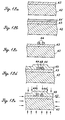
- Figures 12a to 12e show the fabrication process for a seventh embodiment of the present invention.
- a buffer layer 43 is formed on the surface of a substrate 42 which may consist of a wafer made of semiconductor, silica glass or ceramics ( Figure 12a) by the FHD process.
- a core layer 44' essentially consisting of SiO 2 is formed by a low-temperature film-forming process such as the CVD process on the surface of the buffer layer 43.
- the core layer 44' is appropriately doped by using one or more of the dopants selected from a group consisting of phosphorus (P), titanium (Ti), germanium (Ge), aluminum (Al), boron (B) and fluoride (F) for the purpose of increasing the refractive index of the core layer 44' by 0.2 to 0.8% over that of the buffer layer 43.
- Phosphorus (P), titanium (Ti), germanium (Ge) and aluminum (Al) are known to raise the refractive index while boron (B) and fluoride (F) are known to lower the refractive index.
- a desired refractive index can be achieved.
- the refractive index of the core layer 44' is matched with or made to agree with that of the core of the optically fiber that is to be connected to the optical waveguide device.
- the assembly may be subjected to a preliminary heating process at a high pressure or at the atmospheric pressure. Then, a photoresist layer is placed on the surface of the core layer 44' in a prescribed waveguide pattern and an etching process such as the RIE process is conducted on the core layer 44' to form a core 44 in the prescribed pattern ( Figure 12c).
- an upper clad layer 45 essentially consisting of SiO 2 and having a relatively low refractive index is placed on the surface of the core 44 and the buffer layer 43 by the FHD process ( Figure 12d).
- the refractive index of the upper clad layer 43 may be identical to that of the buffer layer 43 which is lower than that of the core 44.
- voids 48 tend to develop in the upper clad layer 45 particularly in the regions between adjacent segments of the core 44. This is particularly pronounced when an adequate amount of dopant for lowering the softening point is not added to the upper clad layer 45.
- the device 41 is subjected to the HIP process with the surface of the core layer 44' exposed so as to reduce or eliminate the voids 48 and remove the internal stresses that may have developed in the substrate 42, the buffer layer 43, the core 44 and the upper clad layer 45 during the preceding film-forming steps ( Figure 12e).
- the assembly is then cut into the desired size and shape, and the input and output ends of the device are polished into optical planes.
- the temperature and pressure conditions for eliminating voids substantially agreed to those which were observed when the similar experiments were conducted on the device which were based strictly on the low-temperature film-forming process as opposed to the combination of the low-temperature film-forming process and the FHD process.
- the conditions may vary depending on the kinds and amounts of dopants that are added to the upper clad layer to control the softening point thereof.
- the pressure and temperature should be selected as low as possible so long as voids can be eliminated to a tolerable level.
- the HIP process can be applied to the device without using any protective layer if any excessive pressure or temperature is not selected for the HIP process.
Landscapes
- Physics & Mathematics (AREA)
- Engineering & Computer Science (AREA)
- Microelectronics & Electronic Packaging (AREA)
- General Physics & Mathematics (AREA)
- Optics & Photonics (AREA)
- Optical Integrated Circuits (AREA)
Abstract
Description
Claims (20)
- A method for fabricating a planar optical waveguide device having a plurality of core segments formed between a lower clad layer and an upper clad layer, comprising the steps of:preparing a lower clad layer (2) consisting of a glass substrate;forming a core layer (4') on said lower clad layer;patterning said core layer into a plurality of core segments (4);forming an upper clad layer (5) on said lower clad layer and said core segments; andconducting a hot isostatic pressing process on an assembly of said lower clad layer, core segments and upper clad layer at a temperature higher than 800 °C and a pressure higher than 1,000 kgf/cm2.
- A method for a planar optical waveguide device according to claim 1, wherein said core layer is formed by a low-temperature film-forming process.
- A method for fabricating a planar optical waveguide device according to claim 1, wherein said upper clad layer is formed by a low-temperature film-forming process.
- A method for fabricating a planar optical waveguide device according to claim 1, wherein said core layer is formed by a flame hydrolysis deposition process.
- A method for fabricating a planar optical waveguide device according to claim 1, wherein said upper clad layer is formed by a flame hydrolysis deposition process.
- A method for fabricating a planar optical waveguide device according to claim 1, wherein said hot isostatic pressing process is conducted with an outer surface of said upper clad layer substantially exposed.
- A method for fabricating a planar optical waveguide device having a plurality of core segments formed between a lower clad layer and an upper clad layer, comprising the steps of:preparing a lower clad layer (23, 43);forming a core layer on said lower clad layer (24', 44');patterning said core layer into a plurality of core segments (24, 44);forming an upper clad layer (25, 45) on said lower clad layer and said core segments; andconducting a hot isostatic pressing process on an assembly of said lower clad layer, core segments and upper clad layer at a temperature higher than 800 °C and a pressure higher than 1,000 kgf/cm2;at least one of said lower clad layer, core layer and upper clad layer being formed by a flame hydrolysis process.
- A method for fabricating a planar optical waveguide device according to claim 7, wherein said lower clad layer consists of a buffer layer formed on a substrate.
- A method for fabricating a planar optical waveguide device according to claim 7, wherein said lower clad layer consists of a glass substrate.
- A method for fabricating a planar optical waveguide device according to claim 7, said lower clad layer, core layer and upper clad layer are all formed by a flame hydrolysis deposition process.
- A method for fabricating a planar optical waveguide device according to claim 7, at least one of said lower clad layer, core layer and upper clad layer are formed by a flame hydrolysis deposition process while the remaining layers are formed by a low-temperature film-forming process.
- A method for fabricating a planar optical waveguide device according to claim 7, wherein said hot isostatic pressing process is conducted with an outer surface of said upper clad layer substantially exposed.
- A method for fabricating a planar optical waveguide device having a plurality of core segments formed between a lower clad layer and an upper clad layer, comprising the steps of:preparing a lower clad layer (2, 3, 23, 43) ;forming a core layer on said lower clad layer (4', 24', 44');patterning said core layer into a plurality of core segments (4, 24, 44);forming an upper clad layer (5, 25, 45) on said lower clad layer and said core segments; andconducting a hot isostatic pressing process on an assembly of said lower clad layer, core segments and upper clad layer, with an outer surface of said upper clad layer substantially exposed, at a temperature higher than 800 °C and a pressure higher than 1,000 kgf/cm2.
- A method for fabricating a planar optical waveguide device having a plurality of core segments formed between a lower clad layer and an upper clad layer, comprising the steps of:preparing a lower clad layer (12, 13, 33);forming a recess (12a, 13a, 33a) corresponding to a desired pattern of core segments in said lower clad layer;forming a core layer (14', 34') on said lower clad layer including an interior of said recess;conducting a hot isostatic pressing process on an assembly of said lower clad layer and said core layer at a temperature higher than 800 °C and a pressure higher than 1,000 kgf/cm2;removing a surface layer from an assembly of said lower clad layer and said core layer until a surface of said lower clad layer is exposed, and said lower clad layer and said core layer in said recess jointly define a planar surface; andforming an upper clad layer (15, 35) on said planar surface jointly defined by said lower clad layer and said core layer.
- A method for fabricating a planar optical waveguide device according to claim 14, wherein said lower clad layer consists of a substrate (12).
- A method for fabricating a planar optical waveguide device according to claim 14, wherein said lower clad layer consists of a buffer layer (13, 33) formed on a substrate (12, 32).
- A method for fabricating a planar optical waveguide device according to claim 14, said lower clad layer, core layer and upper clad layer are all formed by a flame hydrolysis deposition process.
- A method for fabricating a planar optical waveguide device according to claim 14, said lower clad layer, core layer and upper clad layer are all formed by a low-temperature film-forming process.
- A method for fabricating a planar optical waveguide device according to claim 14, at least one of said lower clad layer, core layer and upper clad layer are formed by a flame hydrolysis deposition process while the remaining layers are formed by a low-temperature film-forming process.
- A method for fabricating a planar optical waveguide device according to claim 14, wherein said hot isostatic pressing process is conducted with an outer surface of said core layer substantially exposed.
Applications Claiming Priority (8)
| Application Number | Priority Date | Filing Date | Title |
|---|---|---|---|
| JP22431299 | 1999-08-06 | ||
| JP22431299 | 1999-08-06 | ||
| JP2000128092 | 2000-04-27 | ||
| JP2000128082 | 2000-04-27 | ||
| JP2000128092A JP2001311845A (en) | 2000-04-27 | 2000-04-27 | Manufacturing method of optical waveguide |
| JP2000128082A JP2001311844A (en) | 2000-04-27 | 2000-04-27 | Manufacturing method of optical waveguide |
| JP2000206107 | 2000-07-07 | ||
| JP2000206107A JP2001116942A (en) | 1999-08-06 | 2000-07-07 | Manufacturing method of optical waveguide |
Publications (2)
| Publication Number | Publication Date |
|---|---|
| EP1074864A2 true EP1074864A2 (en) | 2001-02-07 |
| EP1074864A3 EP1074864A3 (en) | 2001-08-16 |
Family
ID=27477125
Family Applications (1)
| Application Number | Title | Priority Date | Filing Date |
|---|---|---|---|
| EP00202766A Withdrawn EP1074864A3 (en) | 1999-08-06 | 2000-08-04 | Method of fabricating planar optical waveguide devices |
Country Status (2)
| Country | Link |
|---|---|
| EP (1) | EP1074864A3 (en) |
| CA (1) | CA2314957A1 (en) |
Cited By (4)
| Publication number | Priority date | Publication date | Assignee | Title |
|---|---|---|---|---|
| WO2003012497A1 (en) * | 2001-07-31 | 2003-02-13 | Asahi Optronics, Ltd. | Quartz-plane light circuit element and process for producing the same |
| EP1659430A4 (en) * | 2003-03-28 | 2008-10-15 | Omron Tateisi Electronics Co | Optical waveguide circuit component and production method therefor |
| CN104090334A (en) * | 2014-07-30 | 2014-10-08 | 四川飞阳科技有限公司 | Method for preparing core film of planar optical waveguide device |
| US9446138B2 (en) | 2007-02-16 | 2016-09-20 | Ktb Tumorforschungsgesellschaft Mbh | Dual acting prodrugs |
Family Cites Families (5)
| Publication number | Priority date | Publication date | Assignee | Title |
|---|---|---|---|---|
| US4789389A (en) * | 1987-05-20 | 1988-12-06 | Corning Glass Works | Method for producing ultra-high purity, optical quality, glass articles |
| JP3137165B2 (en) * | 1994-08-02 | 2001-02-19 | 日本電信電話株式会社 | Manufacturing method of optical waveguide circuit |
| US5858051A (en) * | 1995-05-08 | 1999-01-12 | Toshiba Machine Co., Ltd. | Method of manufacturing optical waveguide |
| JPH10197737A (en) * | 1997-01-09 | 1998-07-31 | Nippon Telegr & Teleph Corp <Ntt> | Manufacturing method of optical waveguide circuit |
| JP3299700B2 (en) * | 1997-10-22 | 2002-07-08 | 日本発条株式会社 | Manufacturing method of optical waveguide |
-
2000
- 2000-08-03 CA CA002314957A patent/CA2314957A1/en not_active Abandoned
- 2000-08-04 EP EP00202766A patent/EP1074864A3/en not_active Withdrawn
Cited By (5)
| Publication number | Priority date | Publication date | Assignee | Title |
|---|---|---|---|---|
| WO2003012497A1 (en) * | 2001-07-31 | 2003-02-13 | Asahi Optronics, Ltd. | Quartz-plane light circuit element and process for producing the same |
| EP1659430A4 (en) * | 2003-03-28 | 2008-10-15 | Omron Tateisi Electronics Co | Optical waveguide circuit component and production method therefor |
| US9446138B2 (en) | 2007-02-16 | 2016-09-20 | Ktb Tumorforschungsgesellschaft Mbh | Dual acting prodrugs |
| US9901644B2 (en) | 2007-02-16 | 2018-02-27 | Ktb Tumorforschungsgesellschaft Mbh | Dual acting prodrugs |
| CN104090334A (en) * | 2014-07-30 | 2014-10-08 | 四川飞阳科技有限公司 | Method for preparing core film of planar optical waveguide device |
Also Published As
| Publication number | Publication date |
|---|---|
| EP1074864A3 (en) | 2001-08-16 |
| CA2314957A1 (en) | 2001-02-06 |
Similar Documents
| Publication | Publication Date | Title |
|---|---|---|
| US6605228B1 (en) | Method for fabricating planar optical waveguide devices | |
| JP3299700B2 (en) | Manufacturing method of optical waveguide | |
| US6690872B2 (en) | Silica based optical waveguide and production method therefor | |
| US6795631B2 (en) | Optical waveguide apparatus and method of producing the same | |
| CA2314957A1 (en) | Method for fabricating planar optical waveguide devices | |
| US6735370B1 (en) | Waveguide for an optical circuit and method of fabrication thereof | |
| AU729257B2 (en) | Method of fabricating an optical component and optical component made thereby | |
| JPH05100123A (en) | Production of optical waveguide | |
| JP3070018B2 (en) | Quartz optical waveguide and method of manufacturing the same | |
| US7221844B2 (en) | Optical waveguide circuit component and method of manufacturing the same | |
| JP2001116942A (en) | Manufacturing method of optical waveguide | |
| JPS60159804A (en) | Optical element adapted to disperse light depending on wavelength | |
| JP2827657B2 (en) | Glass waveguide and manufacturing method thereof | |
| JP2002040275A (en) | Manufacturing method of optical waveguide | |
| JP2001074959A (en) | Embedded optical waveguide and method of manufacturing the same | |
| JP2682919B2 (en) | Optical waveguide and method of manufacturing the same | |
| JP3659278B2 (en) | Manufacturing method of substrate for optical waveguide | |
| JP2927597B2 (en) | Manufacturing method of glass waveguide | |
| JPS63184707A (en) | Manufacture of planar light waveguide | |
| JPH05257021A (en) | Production of optical waveguide | |
| JP2001311845A (en) | Manufacturing method of optical waveguide | |
| JP3689031B2 (en) | Optical waveguide and method for manufacturing the same | |
| JP2001311844A (en) | Manufacturing method of optical waveguide | |
| KR20020040551A (en) | Optical waveguide and manufacturing method thereof | |
| JPH06174952A (en) | Substrate type optical waveguide and its production |
Legal Events
| Date | Code | Title | Description |
|---|---|---|---|
| PUAI | Public reference made under article 153(3) epc to a published international application that has entered the european phase |
Free format text: ORIGINAL CODE: 0009012 |
|
| AK | Designated contracting states |
Kind code of ref document: A2 Designated state(s): DE FR GB |
|
| AX | Request for extension of the european patent |
Free format text: AL;LT;LV;MK;RO;SI |
|
| PUAL | Search report despatched |
Free format text: ORIGINAL CODE: 0009013 |
|
| AK | Designated contracting states |
Kind code of ref document: A3 Designated state(s): AT BE CH CY DE DK ES FI FR GB GR IE IT LI LU MC NL PT SE |
|
| AX | Request for extension of the european patent |
Free format text: AL;LT;LV;MK;RO;SI |
|
| 17P | Request for examination filed |
Effective date: 20020118 |
|
| AKX | Designation fees paid |
Free format text: DE FR GB |
|
| 17Q | First examination report despatched |
Effective date: 20050310 |
|
| STAA | Information on the status of an ep patent application or granted ep patent |
Free format text: STATUS: THE APPLICATION IS DEEMED TO BE WITHDRAWN |
|
| 18D | Application deemed to be withdrawn |
Effective date: 20050721 |