EP1073125A2 - Integrated semiconductor optic sensor device and corresponding manufacturing process - Google Patents
Integrated semiconductor optic sensor device and corresponding manufacturing process Download PDFInfo
- Publication number
- EP1073125A2 EP1073125A2 EP00104800A EP00104800A EP1073125A2 EP 1073125 A2 EP1073125 A2 EP 1073125A2 EP 00104800 A EP00104800 A EP 00104800A EP 00104800 A EP00104800 A EP 00104800A EP 1073125 A2 EP1073125 A2 EP 1073125A2
- Authority
- EP
- European Patent Office
- Prior art keywords
- layers
- photosensor
- layer
- stack
- sensor device
- Prior art date
- Legal status (The legal status is an assumption and is not a legal conclusion. Google has not performed a legal analysis and makes no representation as to the accuracy of the status listed.)
- Withdrawn
Links
Images
Classifications
-
- H—ELECTRICITY
- H10—SEMICONDUCTOR DEVICES; ELECTRIC SOLID-STATE DEVICES NOT OTHERWISE PROVIDED FOR
- H10F—INORGANIC SEMICONDUCTOR DEVICES SENSITIVE TO INFRARED RADIATION, LIGHT, ELECTROMAGNETIC RADIATION OF SHORTER WAVELENGTH OR CORPUSCULAR RADIATION
- H10F77/00—Constructional details of devices covered by this subclass
- H10F77/30—Coatings
- H10F77/306—Coatings for devices having potential barriers
- H10F77/331—Coatings for devices having potential barriers for filtering or shielding light, e.g. multicolour filters for photodetectors
- H10F77/337—Coatings for devices having potential barriers for filtering or shielding light, e.g. multicolour filters for photodetectors using interference filters, e.g. multilayer dielectric filters
-
- G—PHYSICS
- G01—MEASURING; TESTING
- G01J—MEASUREMENT OF INTENSITY, VELOCITY, SPECTRAL CONTENT, POLARISATION, PHASE OR PULSE CHARACTERISTICS OF INFRARED, VISIBLE OR ULTRAVIOLET LIGHT; COLORIMETRY; RADIATION PYROMETRY
- G01J3/00—Spectrometry; Spectrophotometry; Monochromators; Measuring colours
- G01J3/46—Measurement of colour; Colour measuring devices, e.g. colorimeters
- G01J3/50—Measurement of colour; Colour measuring devices, e.g. colorimeters using electric radiation detectors
- G01J3/51—Measurement of colour; Colour measuring devices, e.g. colorimeters using electric radiation detectors using colour filters
- G01J3/513—Measurement of colour; Colour measuring devices, e.g. colorimeters using electric radiation detectors using colour filters having fixed filter-detector pairs
- G01J2003/516—Measurement of colour; Colour measuring devices, e.g. colorimeters using electric radiation detectors using colour filters having fixed filter-detector pairs with several stacked filters or stacked filter-detector pairs
Definitions
- the present invention relates to an integrated semiconductor optic sensor device having a desired spectral selectivity and obtained by a standard CMOS process.
- the invention also relates to a process for manufacturing an optic sensor device by a standard CMOS process, including at least the following phases:
- One of the most inportant field of application of the invention is the process for manufacturing a matrix of integrated colour sensitive photosensors, for instance for colour images or colour television camera.
- optical light sensors based on semiconductor properties are widely used for several video image applications.
- a series of coloured filters is generally provided between the light source and the photosensitive device.
- This is usually implemented by a deposition of an organic coloured resin over the finished semiconductor photosensitive device. This resin stops by absorption all the unwanted colours of the incident light and transmits to the light sensor just the light wavelengths to be selected. In this manner the electric signal generated in the semiconductor device is correlated to the selected colour only.
- the photodiodes are integrated on silicon to form a bidimensional matrix. From the top view each diode looks squared. Each diode is electrically insulated from the other adjacent diodes by an isolation region, for instance field oxide.
- the semiconductor matrix includes at least three different kind of staggered diodes, which are sensible to blue, green and red light respectively.
- the main drawback of the photodiodes covered by the organic resin is due to the fact that the manufacturing process step for the resin deposition is a further process step and that the filter absorbs a portion of the incident light reducing the diode sensibility. Morover, long exposure to intense light, humidity, high temperature and ionising radiation may reduce the ability of the organic resins to stop the unwanted colours.
- this method provides the deposition of a stack of inorganic layers over the light sensor device. These layers have suitable thicknesses and indexes of refraction.
- Modulating the interference of the light waves reflected at all the layers interfaces of the stack it is possible to maximize or minimize the light intensity transmitted or reflected by the whole stack in pre-determined wavelength ranges, that is colours.
- the incident light is reflected by the interface monosilicon/oxide and interferes with the light reflected by the other interface oxide/polysilicon.
- the above disclosed method of wavelenght selection by interference determines a better reliability of the sensor, due to the degradation tendency of conventional organic resins. This better reliability is appreciated in those application fields wherein a high temperature or humidity is present, or in cases of high light exposure of the sensor, or even in presence of ionizing radiations.
- the interferential technique can be integrated in standard VLSI semiconductor processes without the need of a dedicated and separeted process and environment to apply colour selecting resins on the finished sensor.
- interferential stacks are formed by materials having a high and a low refraction index, respectively.
- Polysilicon, or amorfous silicon is generally used as high refraction index material, while silicon dioxide is commonly used as low index material.
- Polysilicon leads to an intrinsic parasitic absorption of light that involves a consequent loss of a portion of the optical signal before it reaches the sensor.
- the aim of the present invention is that of preserving the interferential properties and avoiding absorption of light within the interferenrial stack.
- a further object of the present invention is that of using a high refraction index layer having the highest possible transparency in order to improve the current interferential applications, such as video cameras, and to greatly widen the field of application of integrated interferential photodetectors.
- a further aim of the invention is that of improving the spectral sensitivity of the photodetectors that is not available with the standard coloured resins or with interferential integrated stacks of known type that make use of the polysilicon layer.
- a further aim of the invention is that of rendering more flexible the design of resonators by the possibility of making more complex interferential stacks with any number of high refraction index layers and low refraction index layers, thereby achieving a wide range of spectral transmission curves.
- the solution idea behind the present invention is that of using a transparent metallic oxide having a high dielectric constant as the high refraction index layer of the multilayer interferential filter.
- the invention relates to process for manufacturing a light sensor device in a standard CMOS process, including at least the following phases:
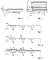
- Figure 1 generally and schematically shown in Figure 1 is a light sensor device 1 including an interferential coloured filter 9 according to the present invention.
- the light sensor device 1 may be considered an integrated photodiode which is realized over a semiconductor substrate 2 region of a first conductivity type, for instance a P doped semiconductor region.
- This semiconductor substrate 2 hosts other CMOS circuit components, which are realized according to a conventional and standard CMOS process flow.
- the substrate 2 is formed by monocristalline silicon and will be disclosed hereinafter as a monosilicon substrate.
- the photodiode 1 comprises a first region formed by the monocristalline silicon of the substrate and a second monocristalline region having a doping type, opposite to the substrate.
- a stack formed by a multilayer structure including:
- a further and optional layer 6 formed by a silicon nitride layer it might be advisable to use a further and optional layer 6 formed by a silicon nitride layer.
- the monosilicon and the trasparent metallic oxide layers 1, 5 have a high refraction index, while the silicon oxide layer 4 and the optional silicon nitride layer 6 have a low refraction index.
- the thickness of the various layers must be defined to assure an anti-reflection effect and a filtering effect according to a specific light wavelength.
- Figure 3 shows a monosilicon semiconductor portion 2 comprising three different diode cathode regions 1R, 1G, 1B, respectively. These regions will be sensible to Red, Green and Blue colours respectively.
- regions 1R, 1G, 1B are defined by a photolitografic process step that provided for a resist deposition and etching steps followed by a Source/Drain implantation of the diodes active areas uncovered by dielectric, as in a standard CMOS process.
- silicon oxide layers having different thickness are deposited over these three regions 1R, 1G, 1B.
- a first process step shown in Figure 3 provides for the deposition of a first oxide layer 4-1 just over the first cathode region 1R.
- a blanket oxide deposition is performed over the substrate 2 surface. Then a mask is provided to protect the area of the cathode region 1R where the Red photosensor must be formed. A subsequent oxide etching and resist mask removal clears the area out from region 1R.
- a further process step is then performed to cover with a second oxide layer 4-2 the second cathode region 1G and the first oxide layer 4-1, as clearly shown in Figure 4.
- a blanket oxide deposition is then performed over the semiconductor.
- a mask is provided to protect the area of the cathode regions 1R and 1G where the Red and the Green photosensors must be formed.
- a subsequent oxide etching and resist mask removal clears the area out from regions 1R and 1G.
- the inventive process is proceeded with a further oxide deposition step to cover with a third oxide layer 4-3 the whole semiconductor portion shown in Figure 5.
- this further oxide layer 4-3 is a protecting (undoped) dielectric layer, for instance a USG type layer, which is normally used as a first layer of premetal dielectric over a polysilicon layer.
- a protecting dielectric layer for instance a USG type layer
- premetal dielectric which is the insulator deposited before metal interconnections
- the premetal dielectric is generally a stack of a first protecting dielectric, undoped and not planarizing, followed by a second planarizing dielectric (usually doped).
- This third oxide layer is not etched between two adjacent photosensors. This allows obtaining a better planarized structure even if the USG oxide is a conformal layer.
- the thicknesses of the three oxide layers may be regulated according to the needs to bring the total thickness of the oxide stacks to a value multiple of the L/2. For instance, it's possible to obtain a layer thickness of nL/2, where n may be an integer number.
- This layer 5 may be for instance a thin layer of titanium oxide (TiO 2 ) having a high transparency and high refraction index.
- TiO 2 titanium oxide
- Other similar materials may be suitable, for instance Ta 2 O 5 , having a high transparency and a high dielectric constant with a consequent high refraction index.
- Refraction index of layer 5 has negligible imaginary component and so being highly transparent, causes a negligible signal loss due to absorption.
- the transparency range includes the visible light as well as near Infra Red IR and near Ultra Violet UV wavelenghts.
- a light sensor device is realised by implanting an active area on the semiconductor substrate in order to obtain at least a first integrated region of corresponding photosensor. Then at least a stack of layers having different thickness and refractive index is formed over this active area to provide an interferential filter for the photosensor.
- the high refraction index layer 5 of said stack are formed by a trasparent metallic oxide having a high refraction index.
- the layer 5 can be obtained through two process steps.
- a first step provides a first deposition of a metallic titanium and a second process step provides for a thermal oxidation cycle in a controlled environment.
- layer 5 The physical properties of layer 5 are specifically advantageous in optical applications between 10E13 and 10E16 Hz.
- layer 5 is not required to have specific electric properties to support electric fields since there is no need to apply any electric field to such a layer 5.
- this layer 5 of transparent metallic oxide improves the signal/noise ratio of the light sensor device with respect to the case in which it is made by polysilicon.
- the inventive process may proceeded with a further deposition step of an optional silicon nitride layer 6.
- An etching step is performed to remove the optional nitride layer 6, when it is present, and the transparent metallic oxide layer 5 out of the regions 1R, 1G and 1B. Then the photoresist mask is removed too.
- the third USG oxide layer 4-3 is not etched thus avoiding a possible overetch and related field oxide consumption with a possible active areas widening on the CMOS circuitry and the consequent reduction of the insulating capability of the field oxide.
- the three stacks are defined over the diode sensors while the active areas of other CMOS circuitry integrated on the same semiconductor substrate 2 remain already covered by the protecting (undoped) dielectric layer 4-3 which is not removed by the last etching step.
- a final process step is then performed to provide a metal dielectric deposition of a BPSG planarizing layer to provide the second planarizing dielectric layer.
- the process according to the present invention allows an improved sensitivity of the sensors in interferential colour selecting sensors.
- This improved sensitivity holds at all optical wavelenghts, but becomes particularly evident for wavelenghts shorter than that of the yellow colour, which means green, blue, violet, near UV radiation down to at least 250 nm.
- Another advantage of the inventive process is to allow more flexibility for the design of interferential resonators due to the possibility of using more than one, and not only very thin, high index layer, in order to get interferential transmission spectra of the desired shape (e.g. narrow integrated interferential pass band filters or any other pre-definited shape required for the desired application.
- the desired shape e.g. narrow integrated interferential pass band filters or any other pre-definited shape required for the desired application.
- a related advantage is given by the possibility offered by the invention to realize a very wide range of spectral transmission curves since the interferential stack can be designed to fit to spectral stransmission shape needed having used a high index transparent material.
Landscapes
- Light Receiving Elements (AREA)
- Solid State Image Pick-Up Elements (AREA)
Abstract
Description
- implanting active areas on a semiconductor substrate to obtain at least a first integrated region of a corresponding photosensor;
- forming at least a stack of layers having different thickness and
refractive index over said photosensor to provide an interferential filter
for said photosensor;
wherein: - at least one of said layers is formed by a trasparent metallic oxide having a high refraction index.
- Figure 1 is a schematic view of a vertical cross section of a semiconductor portion including a light sensor device manufactured according to the present invention;
- Figure 2 is a schematic view of a vertical cross section of a semiconductor portion including a light sensor device according to a further embodiment of the present invention;
- Figure 3 is a schematic view of a vertical cross section of a semiconductor portion at the beginning of the inventive manufacturing process;
- Figure 4 is a schematic view of a vertical cross section of a semiconductor portion during further process step of the manufacturing process according to the present invention;
- Figure 5 is a schematic view of a vertical cross section of a semiconductor portion including at least three photodiodes obtained with the manufacturing process according to the invention.
- A low refractive index dielectric layer, such as a
silicon oxide layer 4; - a high
refractive index layer 5, for instance a transparent metallic oxide having a high refraction index and a corresponding high dielectric constant.
Claims (9)
- A process for manufacturing an optic sensor device by a standard CMOS process, including at least the following phases:implanting active areas on a semiconductor substrate to obtain at least a first integrated region of a corresponding photosensor;forming at least a stack of layers having different thickness and refractive index over said photosensor to provide an interferential filter for said photosensor;
wherein:at least one (5) of said layers is formed by a trasparent metallic oxide having a high refraction index. - Process according to claim 1, wherein said at least one of said layers is a titanium oxide layer.
- Process according to claim 1, wherein said at least one of said layers is a tantalium oxide layer.
- Process according to claim 1, wherein a further deposition step of a silicon nitride layer is provided over said layer.
- Process according to claim 1, wherein a second and a third integrated regions of corresponding photosensors are provided on said substrate and that said stack of layers cover said further regions.
- Process according to claim 1, wherein said stack is a formed by a plurality of oxide layers (4) having a low refraction index each one covered by one layer (5) having a high refraction index.
- An optic sensor device obtained by a standard CMOS process and including:at least a first integrated region on a semiconductor substrate for a corresponding photosensor;at least a stack of layers having different thickness and refractive index over said photosensor to provide an interferential filter of the desired spectral transmission shape for said photosensor;
wherein:At least one (5) of said layers is formed by a trasparent metallic oxide having a high refraction index. - An optic sensor device according to claim 8, wherein said at least one of layers is a titanium oxide layer.
- An optic sensor device according to claim 8, wherein said at least one of layers is a tantalium oxide layer.
Priority Applications (2)
| Application Number | Priority Date | Filing Date | Title |
|---|---|---|---|
| US09/626,836 US6352876B1 (en) | 1999-07-28 | 2000-07-27 | Integrated semiconductor optic sensor device and corresponding manufacturing process |
| US09/972,169 US6538267B2 (en) | 1999-07-28 | 2001-10-03 | Integrated semiconductor optic sensor device |
Applications Claiming Priority (2)
| Application Number | Priority Date | Filing Date | Title |
|---|---|---|---|
| IT1999MI001680A IT1313260B1 (en) | 1999-07-28 | 1999-07-28 | INTEGRATED PHOTOSENSOR DEVICE ON SEMICONDUCTOR AND RELATIVE MANUFACTURING PROCESS. |
| ITMI991680 | 1999-07-28 |
Publications (2)
| Publication Number | Publication Date |
|---|---|
| EP1073125A2 true EP1073125A2 (en) | 2001-01-31 |
| EP1073125A3 EP1073125A3 (en) | 2003-10-08 |
Family
ID=11383438
Family Applications (1)
| Application Number | Title | Priority Date | Filing Date |
|---|---|---|---|
| EP00104800A Withdrawn EP1073125A3 (en) | 1999-07-28 | 2000-03-06 | Integrated semiconductor optic sensor device and corresponding manufacturing process |
Country Status (2)
| Country | Link |
|---|---|
| EP (1) | EP1073125A3 (en) |
| IT (1) | IT1313260B1 (en) |
Cited By (12)
| Publication number | Priority date | Publication date | Assignee | Title |
|---|---|---|---|---|
| RU2224331C2 (en) * | 2001-11-23 | 2004-02-20 | Институт физики им. Л.В.Киренского СО РАН | Photodetector ( variants ) |
| RU2239918C2 (en) * | 2002-02-08 | 2004-11-10 | Институт физики им. Л.В. Киренского СО РАН | Photodetector |
| EP1414068A3 (en) * | 2002-10-25 | 2005-09-21 | OmniVision International Holding Ltd | Image sensor having integrated thin film infrared filter |
| EP1341235A3 (en) * | 2002-02-28 | 2006-05-10 | Canon Kabushiki Kaisha | Image pickup apparatus |
| JP2006190958A (en) * | 2004-12-10 | 2006-07-20 | Sony Corp | Physical information acquisition method and physical information acquisition device |
| EP1592067A4 (en) * | 2004-01-15 | 2007-05-02 | Matsushita Electric Industrial Co Ltd | SOLID STATE IMAGING DEVICE, METHOD FOR PRODUCING THE SOLID STATE IMAGING DEVICE, AND CAMERA USING THE SAME |
| WO2008097705A1 (en) * | 2007-02-09 | 2008-08-14 | Intersil Americas Inc. | Ambient light detectors using conventional cmos image sensor process |
| US8101901B2 (en) | 2004-12-10 | 2012-01-24 | Sony Corporation | Method and apparatus for acquiring physical information, method for manufacturing semiconductor device including array of a plurality of unit components for detecting physical quantity distribution, light-receiving device and manufacturing method therefor, and solid-state imaging device and manufacturing method therefor |
| US8492699B2 (en) | 2009-09-22 | 2013-07-23 | Intersil Americas Inc. | Photodetectors useful as ambient light sensors having an optical filter rejecting a portion of infrared light |
| TWI416948B (en) * | 2006-02-27 | 2013-11-21 | Mitsumasa Koyanagi | Multilayer semiconductor device loaded with integrated sensor |
| US8779542B2 (en) | 2012-11-21 | 2014-07-15 | Intersil Americas LLC | Photodetectors useful as ambient light sensors and methods for use in manufacturing the same |
| CN118156277A (en) * | 2022-12-06 | 2024-06-07 | 豪威科技股份有限公司 | Multi-layer reflective stack and its manufacturing process for reducing crosstalk in split-pixel image sensors |
Family Cites Families (4)
| Publication number | Priority date | Publication date | Assignee | Title |
|---|---|---|---|---|
| JPS62119502A (en) * | 1985-11-18 | 1987-05-30 | インタ−ナショナル ビジネス マシ−ンズ コ−ポレ−ション | Spectrum-filter |
| US5453611A (en) * | 1993-01-01 | 1995-09-26 | Canon Kabushiki Kaisha | Solid-state image pickup device with a plurality of photoelectric conversion elements on a common semiconductor chip |
| JP3242495B2 (en) * | 1993-07-01 | 2001-12-25 | シャープ株式会社 | Photodetector with multilayer filter and method of manufacturing the same |
| US5648653A (en) * | 1993-10-22 | 1997-07-15 | Canon Kabushiki Kaisha | Optical filter having alternately laminated thin layers provided on a light receiving surface of an image sensor |
-
1999
- 1999-07-28 IT IT1999MI001680A patent/IT1313260B1/en active
-
2000
- 2000-03-06 EP EP00104800A patent/EP1073125A3/en not_active Withdrawn
Cited By (18)
| Publication number | Priority date | Publication date | Assignee | Title |
|---|---|---|---|---|
| RU2224331C2 (en) * | 2001-11-23 | 2004-02-20 | Институт физики им. Л.В.Киренского СО РАН | Photodetector ( variants ) |
| RU2239918C2 (en) * | 2002-02-08 | 2004-11-10 | Институт физики им. Л.В. Киренского СО РАН | Photodetector |
| EP1341235A3 (en) * | 2002-02-28 | 2006-05-10 | Canon Kabushiki Kaisha | Image pickup apparatus |
| US7245324B2 (en) | 2002-02-28 | 2007-07-17 | Canon Kabushiki Kaisha | Image pickup apparatus for photographing an object |
| EP1414068A3 (en) * | 2002-10-25 | 2005-09-21 | OmniVision International Holding Ltd | Image sensor having integrated thin film infrared filter |
| US7388242B2 (en) | 2002-10-25 | 2008-06-17 | Omnivision International Holding Ltd. | Image sensor having integrated thin film infrared filter |
| US7759679B2 (en) | 2004-01-15 | 2010-07-20 | Panasonic Corporation | Solid-state imaging device, manufacturing method of solid-state imaging device, and camera employing same |
| EP1592067A4 (en) * | 2004-01-15 | 2007-05-02 | Matsushita Electric Industrial Co Ltd | SOLID STATE IMAGING DEVICE, METHOD FOR PRODUCING THE SOLID STATE IMAGING DEVICE, AND CAMERA USING THE SAME |
| US8101901B2 (en) | 2004-12-10 | 2012-01-24 | Sony Corporation | Method and apparatus for acquiring physical information, method for manufacturing semiconductor device including array of a plurality of unit components for detecting physical quantity distribution, light-receiving device and manufacturing method therefor, and solid-state imaging device and manufacturing method therefor |
| JP2006190958A (en) * | 2004-12-10 | 2006-07-20 | Sony Corp | Physical information acquisition method and physical information acquisition device |
| TWI416948B (en) * | 2006-02-27 | 2013-11-21 | Mitsumasa Koyanagi | Multilayer semiconductor device loaded with integrated sensor |
| WO2008097705A1 (en) * | 2007-02-09 | 2008-08-14 | Intersil Americas Inc. | Ambient light detectors using conventional cmos image sensor process |
| US7960807B2 (en) | 2007-02-09 | 2011-06-14 | Intersil Americas Inc. | Ambient light detectors using conventional CMOS image sensor process |
| CN101611626B (en) * | 2007-02-09 | 2011-06-29 | 英特赛尔美国股份有限公司 | Ambient Light Detector Utilizing Conventional CMOS Image Sensor Process |
| US8492699B2 (en) | 2009-09-22 | 2013-07-23 | Intersil Americas Inc. | Photodetectors useful as ambient light sensors having an optical filter rejecting a portion of infrared light |
| US8779542B2 (en) | 2012-11-21 | 2014-07-15 | Intersil Americas LLC | Photodetectors useful as ambient light sensors and methods for use in manufacturing the same |
| USRE47503E1 (en) | 2012-11-21 | 2019-07-09 | Intersil Americas LLC | Photodetectors useful as ambient light sensors and methods for use in manufacturing the same |
| CN118156277A (en) * | 2022-12-06 | 2024-06-07 | 豪威科技股份有限公司 | Multi-layer reflective stack and its manufacturing process for reducing crosstalk in split-pixel image sensors |
Also Published As
| Publication number | Publication date |
|---|---|
| ITMI991680A0 (en) | 1999-07-28 |
| EP1073125A3 (en) | 2003-10-08 |
| ITMI991680A1 (en) | 2001-01-28 |
| IT1313260B1 (en) | 2002-07-17 |
Similar Documents
| Publication | Publication Date | Title |
|---|---|---|
| US6538267B2 (en) | Integrated semiconductor optic sensor device | |
| US6830951B2 (en) | Integrated semiconductor light sensor device and corresponding manufacturing process | |
| US7223960B2 (en) | Image sensor, an image sensor pixel, and methods of forming the same | |
| US6979588B2 (en) | Method for manufacturing CMOS image sensor having microlens therein with high photosensitivity | |
| CN101252139B (en) | image sensor | |
| US9711562B2 (en) | Apparatus and method for reducing optical cross-talk in image sensors | |
| US7312093B2 (en) | Image sensor capable of adjusting focusing length for individual color and fabrication method thereof | |
| KR100672994B1 (en) | Image sensor and its manufacturing method | |
| US20090189055A1 (en) | Image sensor and fabrication method thereof | |
| US10910425B2 (en) | Solid-state image sensor | |
| KR100303774B1 (en) | Manufacturing method of CMOS image sensor with improved light sensitivity | |
| US20160254303A1 (en) | Photoelectric conversion device | |
| KR100340068B1 (en) | Image sensor having optical designed layer to improve optical transmittance | |
| TW200810100A (en) | Image sensor and the method for manufacturing the same | |
| CN100590879C (en) | Backside light sensing device and method for forming backside light sensing device | |
| ITMI991680A1 (en) | INTEGRATED PHOTOSENSOR DEVICE ON SEMICONDUCTOR AND RELATED MANUFACTURING PROCESS | |
| KR100540557B1 (en) | Image sensor manufacturing method for improving optical transmission rate | |
| CN110085613A (en) | Image sensor and forming method thereof | |
| US20070051992A1 (en) | CMOS image sensor and method of fabricating the same | |
| KR100486756B1 (en) | Method for fabrication of image sensor | |
| KR100700267B1 (en) | Image sensor and its manufacturing method | |
| KR20010061078A (en) | Method for fabricating image sensor with correct color image | |
| JPS6348234B2 (en) | ||
| US20250331324A1 (en) | Integrated circuit device including a crosstalk reduction structure for half-shield phase detection | |
| KR100683395B1 (en) | Manufacturing method of image sensor for improving light sensitivity |
Legal Events
| Date | Code | Title | Description |
|---|---|---|---|
| PUAI | Public reference made under article 153(3) epc to a published international application that has entered the european phase |
Free format text: ORIGINAL CODE: 0009012 |
|
| AK | Designated contracting states |
Kind code of ref document: A2 Designated state(s): AT BE CH CY DE DK ES FI FR GB GR IE IT LI LU MC NL PT SE |
|
| AX | Request for extension of the european patent |
Free format text: AL;LT;LV;MK;RO;SI |
|
| PUAL | Search report despatched |
Free format text: ORIGINAL CODE: 0009013 |
|
| AK | Designated contracting states |
Kind code of ref document: A3 Designated state(s): AT BE CH CY DE DK ES FI FR GB GR IE IT LI LU MC NL PT SE |
|
| AX | Request for extension of the european patent |
Extension state: AL LT LV MK RO SI |
|
| 17P | Request for examination filed |
Effective date: 20040407 |
|
| AKX | Designation fees paid |
Designated state(s): DE FR GB IT |
|
| 17Q | First examination report despatched |
Effective date: 20040922 |
|
| STAA | Information on the status of an ep patent application or granted ep patent |
Free format text: STATUS: THE APPLICATION IS DEEMED TO BE WITHDRAWN |
|
| 18D | Application deemed to be withdrawn |
Effective date: 20080701 |