EP1073105A2 - Method for wet etching oxides and/or insulators - Google Patents
Method for wet etching oxides and/or insulators Download PDFInfo
- Publication number
- EP1073105A2 EP1073105A2 EP00115887A EP00115887A EP1073105A2 EP 1073105 A2 EP1073105 A2 EP 1073105A2 EP 00115887 A EP00115887 A EP 00115887A EP 00115887 A EP00115887 A EP 00115887A EP 1073105 A2 EP1073105 A2 EP 1073105A2
- Authority
- EP
- European Patent Office
- Prior art keywords
- layer
- etching
- insulating material
- electrical insulating
- providing
- Prior art date
- Legal status (The legal status is an assumption and is not a legal conclusion. Google has not performed a legal analysis and makes no representation as to the accuracy of the status listed.)
- Withdrawn
Links
Images
Classifications
-
- H—ELECTRICITY
- H10—SEMICONDUCTOR DEVICES; ELECTRIC SOLID-STATE DEVICES NOT OTHERWISE PROVIDED FOR
- H10P—GENERIC PROCESSES OR APPARATUS FOR THE MANUFACTURE OR TREATMENT OF DEVICES COVERED BY CLASS H10
- H10P50/00—Etching of wafers, substrates or parts of devices
- H10P50/20—Dry etching; Plasma etching; Reactive-ion etching
- H10P50/28—Dry etching; Plasma etching; Reactive-ion etching of insulating materials
- H10P50/282—Dry etching; Plasma etching; Reactive-ion etching of insulating materials of inorganic materials
- H10P50/283—Dry etching; Plasma etching; Reactive-ion etching of insulating materials of inorganic materials by chemical means
-
- Y—GENERAL TAGGING OF NEW TECHNOLOGICAL DEVELOPMENTS; GENERAL TAGGING OF CROSS-SECTIONAL TECHNOLOGIES SPANNING OVER SEVERAL SECTIONS OF THE IPC; TECHNICAL SUBJECTS COVERED BY FORMER USPC CROSS-REFERENCE ART COLLECTIONS [XRACs] AND DIGESTS
- Y10—TECHNICAL SUBJECTS COVERED BY FORMER USPC
- Y10S—TECHNICAL SUBJECTS COVERED BY FORMER USPC CROSS-REFERENCE ART COLLECTIONS [XRACs] AND DIGESTS
- Y10S438/00—Semiconductor device manufacturing: process
- Y10S438/958—Passivation layer
Definitions
- the present invention pertains to etching electrical insulators and more specifically to etching electrical insulators, such as oxides, on semiconductor surfaces.
- etching processes can be performed by wet or dry etching procedures.
- wet chemistry produces far too much undercutting (i.e. horizontal etching) and is, therefore, not considered for the desired applications.
- some materials are difficult to etch with dry chemistries. Sometimes these materials can be etched, but with little selectivity between the material being etched and the material which is to remain.
- RIE Reactive Ion Etching
- elements that are either very high mass (such as Ba, Sr, Pt, etc.) or highly reactive (such as (Ba, Sr, Ca, etc.).
- Finding volatile byproducts that can be formed during the RIE process is the key to etch selectivity.
- earth metal oxides e.g. SrTiO 3 , BaTiO 3 , and BaSrTiO 3
- Sr and Ti don't make volatile byproducts. So far, the solution has been to use a largely physical etch condition with little or no selectivity. At present, gas chemistry is inferior for these high dielectric constant (high K) materials.
- the desired etch characteristics are vertical sidewalls (large differential etch rates), reasonable etch rates, and high chemical selectivity to other materials that are not to be etched. Vertical sidewalls greater than approximately 80° and selectivity greater than 3 -4 are fairly common. By using a high "physical" component to the RIE etch (e.g. sputtering), near vertical sidewalls are achievable, however, chemical selectivity suffers.
- etch selectivity vertical
- etch selectivity horizontal
- anisotropy the etching of earth metal oxides (including barium titanate, barium strontium titanate, or strontium titanate) which is deposited directly on silicon is desirable. Further, during the etching, any strontium titanate under a gate electrode should remain.
- a focused pattern or a light-stopping mask layer can be used to direct light.
- a mixed solution in which a passivating agent is present along with an etching agent.
- the passivating agent prevents the etching while no light (preferably UV light) is directed at the surface or in areas that the light does not reach.
- no light preferably UV light
- UV light is directed at the surface, the surface passivation is disrupted and etching takes place.
- etching a layer of electrical insulating material in which a thin layer of strontium titanate is provided on a surface of a semiconductor substrate and an acid solution containing less than 1000 ppm of HF is used as the passivated etching solution.
- the layer of strontium titanate is immersed in the passivated etching solution and collimated light is directed onto the passivated surface of the layer of strontium titanate at areas to be etched.
- the collimated light depassivates the passivated surface of the strontium titanate and the passivated etching solution etches the layer of strontium titanate only at the surface receiving collimated light.
- etching As described briefly above, it is desirable to provide a new method of etching to solve the various problems prevalent in today's technology.
- the most desirable ingredients of the etching method are: vertical etch profile; horizontal etch control; (anisotropy) and etch selectivity to other materials with respect to the material to be etched.
- strontium titanate including barium, strontium titanate
- any strontium titanate under a gate electrode should remain, i.e. very little or no horizontal etching.
- very little etching of other materials, such as Si, SiO 2 , and Si 3 N 4 should occur in this solution, even when illuminated by light.
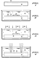
- FIG. 1 illustrates a layer 10 of electrical insulating material on a supporting surface 12, which in this specific example is a layer of strontium titanate on a silicon substrate (e.g. a silicon wafer).
- layer 10 can be any insulating material which is otherwise difficult to etch and, specifically, the insulating material of layer 10 includes oxides and/or high mass materials, such as Ba, St, Pt, etc., and/or highly reactive materials, such as Ba, Sr, Ca, etc.
- etching solution 15 is a solution which contains a passivating material which prevents etching solution 15 from operating on layer 10.
- etching solution 15 includes an etchant or etching material, such as an acid which may be, for example, an acid solution including one of HCl, H 2 SO 4 , HNO 3 , and HPO 3 .
- Etching solution 15, in accordance with the present invention further includes a passivating material, which is any material that passivates the surface of layer 10 to prevent the etchant or etching material from etching layer 10 prior to the application of light, as will be explained in more detail presently.
- a mask 20 is positioned on surface 25 of layer 10 so as to shade all areas which are not to be etched.
- mask 20 can be a hard mask formed directly on surface 25 of layer 10 by any of the well known photolithographic techniques, or it can be a simple shadow mask positioned adjacent to layer 10, or any other structure for preventing light from impinging upon areas of surface 25 which are not to be etched. It will of course be understood that mask 20 should be formed of material which will not be etched by etching solution 15, if it is positioned in etching solution 15.
- supporting surface 12 is a semiconductor material, such as silicon or a silicon containing material and layer 10 is an oxide, for example an alkaline earth oxide such as strontium titanate.
- Etching solution 15 includes an acid, in this specific example HCl, and a passivating material, which in this specific example is HF.
- the HF passivates the etching process so that substantially no etching occurs by simply immersing supporting surface 12 and layer 10 into passivated etching solution 15.
- ppm parts per million
- etching in an etch solution of 12.4 Molar HCl provides the passivation required.
- a relatively small amount e.g. generally several monolayers or less than 10 ⁇
- this etching stops after the initial small etch and does not continue.
- light (represented by arrows 22 in FIG. 3) is directed onto surface 25 of layer 10 to be etched. It is preferred that the light at least include ultra violet (UV) light with an energy approximately equal to or greater than the bandgap of the material to be etched.
- UV ultra violet
- the light also may be tailored to the excitation energy of the passivation bonded to the surface. In a preferred embodiment the light is focused or collimated to be sure that no light inadvertently strikes the sidewalls or other areas which are not to be etched.
- simply using mask 20 positioned directly on surface 25 and a reasonably directable light source may be sufficient to achieve the desired purposes.
- light sources such as light that is at least partially collimated or focused by lenses and apertures, can be used (e.g. stepper light with a reticle mask).
- An example of the use of a focused pattern of light is illustrated in FIG. 4.
- Mercury Arc lamps that are lensed and filtered are preferred for their low cost and high intensity in the UV range. Directing the collimated light onto the surface of layer 10 at areas to be etched, depassivates surface 25 and etching of layer 10, only at the areas receiving collimated light, begins and continues as long as the light is present.
- a solution of straight HCl (12.4 Molar HCl solution) as the etchant generally etches at a rate of 10 ⁇ to 15 ⁇ per minute.
- substantially no etching occurs (except for the small initial etch described above) until the light is applied, after which electrical insulating layer 10 is etched at a rate of greater than 50 ⁇ per minute, and generally in a range of 50 ⁇ to 100 ⁇ per minute.
- electrical insulating layer 10 is etched at a rate of greater than 50 ⁇ per minute, and generally in a range of 50 ⁇ to 100 ⁇ per minute.
- the light is directed only onto the upper surface (initially surface 25) of layer 10 (even as the etch progresses) substantially no horizontal etching occurs and the sidewalls are substantially vertical with no undercutting.
- the high selectivity of strontium titanate, for example, over Si, SiO 2 and other materials allows a large overetch. This overetch allows for areas that are thicker or etch more slowly, to be completely etched while those areas that have already etched through are essentially unaffected by the additional etchant and light exposure.
- the structure can be prepassivated before dipping into passivated etching solution 15.
- This initial passivation or prepassivation can be accomplished by dipping the structure to be etched into a prepassivating solution, which in the specific example described above is water and less than 1000 ppm of HF.
- the time between prepassivation and etching is not believed to be critical, i.e. some time (even days) can pass. It is believed that the prepassivating solution forms an initial passivating layer on the surface of the layer to be etched (e.g.
- any passivation material can be used in either the prepassivation or the passivated etching solutions described above. While HF is used in the specific example, many other materials, such as any organic material, will operate as an etch inhibitor or passivation material in the present process.
- a new and improved method of etching electrical insulators and specifically oxides, is disclosed.
- the new and improved method of etching electrical insulators has improved vertical etch profile, horizontal etch control, (anisotropy) and etch selectivity to other materials with respect to the material to be etched. Further, the new and improved method of etching electrical insulators provides an improved etch rate.
- the new and improved method of etching is used to etch alkaline earth oxides (including SrTiO 3 , BaTiO 3 and BaSrTiO 3 ) on semiconductor substrates including silicon and uses an HCl etching solution with HF as the passivating material.
Landscapes
- Weting (AREA)
Abstract
Description
Claims (10)
- A method of etching a layer of electrical insulating material characterised by the steps of:providing a layer of electrical insulating material (10) on a supporting surface (12);providing an etching solution (15);immersing the layer of electrical insulating material in the etching solution while using a passivating material (20) at a surface of the layer of electrical insulating material to prevent the etching solution from operating on the electrical insulating material; anddirecting light (22) onto the surface of the layer of electrical insulating material at areas to be etched, so as to depassivate the surface and to etch the surface of the layer of electrical insulating material only at the areas receiving light.
- A method of etching a layer of electrical insulating material as claimed in claim 1 wherein the step of providing the layer of electrical insulating material includes providing a layer of oxide.
- A method of etching a layer of electrical insulating material as claimed in claim 2 wherein the step of providing the layer of oxide includes providing an alkaline earth oxide.
- A method of etching a layer of electrical insulating material as claimed in claim 2 wherein the step of providing the layer of oxide includes providing a layer including a titanate.
- A method of etching a layer of electrical insulating material as claimed in claim 4 wherein the step of providing the layer including the titanate includes providing a layer including one of SrTiO3, BaTiO3 and BaSrTiO3.
- A method of etching a layer of electrical insulating material as claimed in claim 1 wherein the step of providing an etching solution includes providing an acid solution.
- A method of etching a layer of electrical insulating material as claimed in claim 6 wherein the step of providing the acid solution includes providing an acid solution including one of HCl, H2SO4, HNO3, and HPO3.
- A method of etching a layer of electrical insulating material as claimed in claim 1 wherein the step of using the passivating material includes using a solution containing HF.
- A method of etching a layer of electrical insulating material as claimed in claim 8 wherein the step of using the solution containing HF includes using a solution containing less than 1000 parts per million of HF.
- A method of etching a layer of electrical insulating material as claimed in claim 8 wherein the step of directing light includes focusing stepper light with a reticle mask.
Applications Claiming Priority (2)
| Application Number | Priority Date | Filing Date | Title |
|---|---|---|---|
| US09/362,251 US6358430B1 (en) | 1999-07-28 | 1999-07-28 | Technique for etching oxides and/or insulators |
| US362251 | 1999-07-28 |
Publications (2)
| Publication Number | Publication Date |
|---|---|
| EP1073105A2 true EP1073105A2 (en) | 2001-01-31 |
| EP1073105A3 EP1073105A3 (en) | 2003-09-10 |
Family
ID=23425333
Family Applications (1)
| Application Number | Title | Priority Date | Filing Date |
|---|---|---|---|
| EP00115887A Withdrawn EP1073105A3 (en) | 1999-07-28 | 2000-07-25 | Method for wet etching oxides and/or insulators |
Country Status (3)
| Country | Link |
|---|---|
| US (1) | US6358430B1 (en) |
| EP (1) | EP1073105A3 (en) |
| JP (1) | JP2001077078A (en) |
Cited By (1)
| Publication number | Priority date | Publication date | Assignee | Title |
|---|---|---|---|---|
| WO2011072706A1 (en) * | 2009-12-18 | 2011-06-23 | Rena Gmbh | Method for removing substrate layers |
Families Citing this family (5)
| Publication number | Priority date | Publication date | Assignee | Title |
|---|---|---|---|---|
| US20040043500A1 (en) * | 2002-08-27 | 2004-03-04 | Rumps J Eric | Wafer-scale microwave digestion apparatus and methods |
| DE10244862B4 (en) * | 2002-09-23 | 2006-09-14 | IHP GmbH - Innovations for High Performance Microelectronics/Institut für innovative Mikroelektronik | Method for producing an electronic component with a praseodymium oxide layer |
| JP3795867B2 (en) * | 2003-01-30 | 2006-07-12 | 株式会社ルネサステクノロジ | Etching apparatus, etching method, and manufacturing method of semiconductor device |
| KR102227003B1 (en) * | 2017-04-27 | 2021-03-11 | 고려대학교 산학협력단 | Method for etching of gallium oxide |
| RU2674118C1 (en) * | 2017-10-20 | 2018-12-04 | Акционерное общество "Ангстрем" (АО "Ангстрем") | Selective barium titanate etchant |
Family Cites Families (13)
| Publication number | Priority date | Publication date | Assignee | Title |
|---|---|---|---|---|
| US3808068A (en) * | 1972-12-11 | 1974-04-30 | Bell Telephone Labor Inc | Differential etching of garnet materials |
| US4597825A (en) | 1982-11-10 | 1986-07-01 | International Business Machines Corporation | Intermediate passivation and cleaning of compound semiconductor surfaces |
| US5643472A (en) | 1988-07-08 | 1997-07-01 | Cauldron Limited Partnership | Selective removal of material by irradiation |
| US5385633A (en) | 1990-03-29 | 1995-01-31 | The United States Of America As Represented By The Secretary Of The Navy | Method for laser-assisted silicon etching using halocarbon ambients |
| JPH0465815A (en) * | 1990-07-06 | 1992-03-02 | Matsushita Electric Ind Co Ltd | Formation of pattern |
| US5201989A (en) * | 1992-04-20 | 1993-04-13 | Texas Instruments Incorporated | Anisotropic niobium pentoxide etch |
| US5238529A (en) * | 1992-04-20 | 1993-08-24 | Texas Instruments Incorporated | Anisotropic metal oxide etch |
| US5238530A (en) * | 1992-04-20 | 1993-08-24 | Texas Instruments Incorporated | Anisotropic titanate etch |
| EP0567063B1 (en) * | 1992-04-20 | 1998-03-04 | Texas Instruments Incorporated | Anisotropic metal oxide etch |
| MX9305898A (en) * | 1992-10-30 | 1995-01-31 | Texas Instruments Inc | ANISOTROPIC PHOTOCHEMICAL ENGRAVING METHOD FOR THE MANUFACTURE OF INTEGRATED CIRCUITS. |
| US5603848A (en) * | 1995-01-03 | 1997-02-18 | Texas Instruments Incorporated | Method for etching through a substrate to an attached coating |
| US5824206A (en) | 1996-06-28 | 1998-10-20 | The United States Of America As Represented By The Secretary Of The Air Force | Photoelectrochemical etching of p-InP |
| US5741431A (en) | 1997-05-15 | 1998-04-21 | Industrial Technology Research Institute | Laser assisted cryoetching |
-
1999
- 1999-07-28 US US09/362,251 patent/US6358430B1/en not_active Expired - Fee Related
-
2000
- 2000-07-24 JP JP2000222079A patent/JP2001077078A/en active Pending
- 2000-07-25 EP EP00115887A patent/EP1073105A3/en not_active Withdrawn
Cited By (2)
| Publication number | Priority date | Publication date | Assignee | Title |
|---|---|---|---|---|
| WO2011072706A1 (en) * | 2009-12-18 | 2011-06-23 | Rena Gmbh | Method for removing substrate layers |
| TWI427693B (en) * | 2009-12-18 | 2014-02-21 | 雷納公司 | Method of removing a substrate layer |
Also Published As
| Publication number | Publication date |
|---|---|
| EP1073105A3 (en) | 2003-09-10 |
| US6358430B1 (en) | 2002-03-19 |
| JP2001077078A (en) | 2001-03-23 |
Similar Documents
| Publication | Publication Date | Title |
|---|---|---|
| US6461974B1 (en) | High temperature tungsten etching process | |
| KR100391877B1 (en) | Method of manufacturing a semiconductor device | |
| US6140024A (en) | Remote plasma nitridation for contact etch stop | |
| US5484740A (en) | Method of manufacturing a III-V semiconductor gate structure | |
| US6331492B2 (en) | Nitridation for split gate multiple voltage devices | |
| EP1062691B1 (en) | Selective wet etching of inorganic antireflective coatings | |
| US6458650B1 (en) | CU second electrode process with in situ ashing and oxidation process | |
| US6268296B1 (en) | Low temperature process for multiple voltage devices | |
| US6358430B1 (en) | Technique for etching oxides and/or insulators | |
| US6511918B2 (en) | Method of structuring a metal-containing layer | |
| JPS63117423A (en) | Method of etching silicon dioxide | |
| US6080032A (en) | Process for low temperature semiconductor fabrication | |
| US6345399B1 (en) | Hard mask process to prevent surface roughness for selective dielectric etching | |
| US7709343B2 (en) | Use of a plasma source to form a layer during the formation of a semiconductor device | |
| EP0567063B1 (en) | Anisotropic metal oxide etch | |
| US6528429B2 (en) | Methods of etching insulative materials, of forming electrical devices, and of forming capacitors | |
| JPH11111695A (en) | Method of forming platinum thin film pattern and method of manufacturing semiconductor device | |
| US6716760B2 (en) | Method for forming a gate of a high integration semiconductor device including forming an etching prevention or etch stop layer and anti-reflection layer | |
| KR100542943B1 (en) | Repair etching method of semiconductor device | |
| JP3678771B2 (en) | Dry etching method | |
| KR100568098B1 (en) | How to Form a Metal Pattern | |
| KR100332647B1 (en) | Method of forming a contact hole in a semiconductor device | |
| KR100236078B1 (en) | Etching method for semiconductor material | |
| DE19906814A1 (en) | Surface material removal, especially for hard mask removal from a semiconductor surface, comprises removing material while protecting the rest of the surface with a temporary layer | |
| Kuo et al. | given. |
Legal Events
| Date | Code | Title | Description |
|---|---|---|---|
| PUAI | Public reference made under article 153(3) epc to a published international application that has entered the european phase |
Free format text: ORIGINAL CODE: 0009012 |
|
| AK | Designated contracting states |
Kind code of ref document: A2 Designated state(s): AT BE CH CY DE DK ES FI FR GB GR IE IT LI LU MC NL PT SE |
|
| AX | Request for extension of the european patent |
Free format text: AL;LT;LV;MK;RO;SI |
|
| PUAL | Search report despatched |
Free format text: ORIGINAL CODE: 0009013 |
|
| AK | Designated contracting states |
Kind code of ref document: A3 Designated state(s): AT BE CH CY DE DK ES FI FR GB GR IE IT LI LU MC NL PT SE |
|
| AX | Request for extension of the european patent |
Extension state: AL LT LV MK RO SI |
|
| RIC1 | Information provided on ipc code assigned before grant |
Ipc: 7H 01L 41/24 B Ipc: 7H 01L 21/465 B Ipc: 7H 01L 21/311 A |
|
| 17P | Request for examination filed |
Effective date: 20040310 |
|
| AKX | Designation fees paid |
Designated state(s): DE FR GB |
|
| 17Q | First examination report despatched |
Effective date: 20040615 |
|
| STAA | Information on the status of an ep patent application or granted ep patent |
Free format text: STATUS: THE APPLICATION IS DEEMED TO BE WITHDRAWN |
|
| 18D | Application deemed to be withdrawn |
Effective date: 20041026 |