EP1071249B1 - Procédé et dispositif de modulation dans un émetteur - Google Patents
Procédé et dispositif de modulation dans un émetteur Download PDFInfo
- Publication number
- EP1071249B1 EP1071249B1 EP00402060A EP00402060A EP1071249B1 EP 1071249 B1 EP1071249 B1 EP 1071249B1 EP 00402060 A EP00402060 A EP 00402060A EP 00402060 A EP00402060 A EP 00402060A EP 1071249 B1 EP1071249 B1 EP 1071249B1
- Authority
- EP
- European Patent Office
- Prior art keywords
- signal
- modulation
- frequency
- circuit
- reference signal
- Prior art date
- Legal status (The legal status is an assumption and is not a legal conclusion. Google has not performed a legal analysis and makes no representation as to the accuracy of the status listed.)
- Expired - Lifetime
Links
- 238000000034 method Methods 0.000 title claims abstract description 18
- 238000001914 filtration Methods 0.000 claims description 17
- 230000005540 biological transmission Effects 0.000 claims description 10
- 230000008859 change Effects 0.000 claims description 9
- 238000006243 chemical reaction Methods 0.000 claims description 6
- 238000000605 extraction Methods 0.000 claims 3
- 230000009977 dual effect Effects 0.000 abstract description 3
- 230000003595 spectral effect Effects 0.000 abstract description 2
- 238000004519 manufacturing process Methods 0.000 abstract 1
- 238000001228 spectrum Methods 0.000 description 12
- 101100219315 Arabidopsis thaliana CYP83A1 gene Proteins 0.000 description 8
- 101000806846 Homo sapiens DNA-(apurinic or apyrimidinic site) endonuclease Proteins 0.000 description 8
- 101000835083 Homo sapiens Tissue factor pathway inhibitor 2 Proteins 0.000 description 8
- 101100269674 Mus musculus Alyref2 gene Proteins 0.000 description 8
- 101100140580 Saccharomyces cerevisiae (strain ATCC 204508 / S288c) REF2 gene Proteins 0.000 description 8
- 102100026134 Tissue factor pathway inhibitor 2 Human genes 0.000 description 8
- 238000010586 diagram Methods 0.000 description 5
- 230000006872 improvement Effects 0.000 description 4
- 230000015654 memory Effects 0.000 description 4
- 230000004048 modification Effects 0.000 description 2
- 238000012986 modification Methods 0.000 description 2
- 244000045947 parasite Species 0.000 description 2
- 230000009467 reduction Effects 0.000 description 2
- 230000017105 transposition Effects 0.000 description 2
- 238000011144 upstream manufacturing Methods 0.000 description 2
- 238000009825 accumulation Methods 0.000 description 1
- 230000000763 evoking effect Effects 0.000 description 1
- 230000014509 gene expression Effects 0.000 description 1
- 238000003780 insertion Methods 0.000 description 1
- 230000037431 insertion Effects 0.000 description 1
- 230000009191 jumping Effects 0.000 description 1
- -1 or a second Proteins 0.000 description 1
- 230000008569 process Effects 0.000 description 1
- 230000005855 radiation Effects 0.000 description 1
- 230000001105 regulatory effect Effects 0.000 description 1
- 230000033764 rhythmic process Effects 0.000 description 1
- 238000005070 sampling Methods 0.000 description 1
- 238000000926 separation method Methods 0.000 description 1
- 230000009466 transformation Effects 0.000 description 1
- 238000000844 transformation Methods 0.000 description 1
Images


Classifications
-
- H—ELECTRICITY
- H03—ELECTRONIC CIRCUITRY
- H03J—TUNING RESONANT CIRCUITS; SELECTING RESONANT CIRCUITS
- H03J5/00—Discontinuous tuning; Selecting predetermined frequencies; Selecting frequency bands with or without continuous tuning in one or more of the bands, e.g. push-button tuning, turret tuner
- H03J5/24—Discontinuous tuning; Selecting predetermined frequencies; Selecting frequency bands with or without continuous tuning in one or more of the bands, e.g. push-button tuning, turret tuner with a number of separate pretuned tuning circuits or separate tuning elements selectively brought into circuit, e.g. for waveband selection or for television channel selection
- H03J5/242—Discontinuous tuning; Selecting predetermined frequencies; Selecting frequency bands with or without continuous tuning in one or more of the bands, e.g. push-button tuning, turret tuner with a number of separate pretuned tuning circuits or separate tuning elements selectively brought into circuit, e.g. for waveband selection or for television channel selection used exclusively for band selection
-
- H—ELECTRICITY
- H03—ELECTRONIC CIRCUITRY
- H03J—TUNING RESONANT CIRCUITS; SELECTING RESONANT CIRCUITS
- H03J5/00—Discontinuous tuning; Selecting predetermined frequencies; Selecting frequency bands with or without continuous tuning in one or more of the bands, e.g. push-button tuning, turret tuner
- H03J5/02—Discontinuous tuning; Selecting predetermined frequencies; Selecting frequency bands with or without continuous tuning in one or more of the bands, e.g. push-button tuning, turret tuner with variable tuning element having a number of predetermined settings and adjustable to a desired one of these settings
- H03J5/0245—Discontinuous tuning using an electrical variable impedance element, e.g. a voltage variable reactive diode, in which no corresponding analogue value either exists or is preset, i.e. the tuning information is only available in a digital form
- H03J5/0272—Discontinuous tuning using an electrical variable impedance element, e.g. a voltage variable reactive diode, in which no corresponding analogue value either exists or is preset, i.e. the tuning information is only available in a digital form the digital values being used to preset a counter or a frequency divider in a phase locked loop, e.g. frequency synthesizer
-
- H—ELECTRICITY
- H04—ELECTRIC COMMUNICATION TECHNIQUE
- H04B—TRANSMISSION
- H04B1/00—Details of transmission systems, not covered by a single one of groups H04B3/00 - H04B13/00; Details of transmission systems not characterised by the medium used for transmission
- H04B1/38—Transceivers, i.e. devices in which transmitter and receiver form a structural unit and in which at least one part is used for functions of transmitting and receiving
- H04B1/40—Circuits
- H04B1/403—Circuits using the same oscillator for generating both the transmitter frequency and the receiver local oscillator frequency
- H04B1/406—Circuits using the same oscillator for generating both the transmitter frequency and the receiver local oscillator frequency with more than one transmission mode, e.g. analog and digital modes
-
- H—ELECTRICITY
- H04—ELECTRIC COMMUNICATION TECHNIQUE
- H04L—TRANSMISSION OF DIGITAL INFORMATION, e.g. TELEGRAPHIC COMMUNICATION
- H04L25/00—Baseband systems
- H04L25/02—Details ; arrangements for supplying electrical power along data transmission lines
- H04L25/03—Shaping networks in transmitter or receiver, e.g. adaptive shaping networks
- H04L25/03828—Arrangements for spectral shaping; Arrangements for providing signals with specified spectral properties
- H04L25/03834—Arrangements for spectral shaping; Arrangements for providing signals with specified spectral properties using pulse shaping
-
- H—ELECTRICITY
- H04—ELECTRIC COMMUNICATION TECHNIQUE
- H04L—TRANSMISSION OF DIGITAL INFORMATION, e.g. TELEGRAPHIC COMMUNICATION
- H04L27/00—Modulated-carrier systems
- H04L27/18—Phase-modulated carrier systems, i.e. using phase-shift keying
- H04L27/20—Modulator circuits; Transmitter circuits
- H04L27/2003—Modulator circuits; Transmitter circuits for continuous phase modulation
- H04L27/2007—Modulator circuits; Transmitter circuits for continuous phase modulation in which the phase change within each symbol period is constrained
- H04L27/2017—Modulator circuits; Transmitter circuits for continuous phase modulation in which the phase change within each symbol period is constrained in which the phase changes are non-linear, e.g. generalized and Gaussian minimum shift keying, tamed frequency modulation
Definitions
- the subject of the present invention is a method of modulation in a transmitter. It also relates to a transmitter operating according to this process.
- the invention is more particularly intended for use with transmitters of the dual band or more generally multiband type. As such she is particularly interesting in the field of mobile telephony when the same transmitter is used to transmit signals according to the 900 MHz GSM standard, the DCS standard at 1800 MHz, the PCS standard at 1900 MHz, or UMTS standard at 2200 MHz.
- the invention has the consequence immediate reduction of the number of local oscillators needed for a multiband mobile phone.
- the modulation circuits used generally, in transmission, in in a control loop an oscillator controlled, usually voltage controlled (VCO), by a signal of control produced by a phase comparator.
- the phase comparator receives a signal at a reference frequency on the one hand and a signal corresponding, after a frequency division by N, to the signal produced by the oscillator controlled in tension on the other hand.
- the frequency of signal produced by the voltage-controlled oscillator is a multiple, by N, of the frequency of the reference signal.
- the frequency of this reference signal is adjusted very precisely, and preferably at a value equal to the difference between two channels of frequency passing in a useful frequency band.
- the separation between channels is 200 KHz so the reference frequency is chosen equal to 200 KHz.
- the division coefficient N used is the order of 4500 in one case and 9000 in the other.
- control loops are not important enough for a same oscillator can serve both in a band, the GSM band at 900 MHz, and in another band, the DCS band at 1800 MHz (or PCS, or UMTS).
- the DCS band at 1800 MHz (or PCS, or UMTS).
- it is necessary to build a second transmission loop with a second local oscillator controlled in tension.
- the solution that subscribes so standards is therefore a more expensive solution because otherwise a local oscillator is a circuit that can not be integrated and which in practice strike very strongly the price of an issuer.
- a divider for example a divider by two.
- high frequencies that can be used in the DCS, PCS or UMTS range can be halved to serve as the central frequencies of channels in the GSM 900 MHz range.
- the divisor can be a divider fractional.
- the document WO 98/25353 relates to a device for transmitting RF signals in two separate frequency bands.
- a first unit of treatment arranged at the output of a VCO is intended for the selection of the operating frequency chosen by the multiplication of the frequency in output of the VCO by a factor k.
- a second processing unit arranged in the phase lock loop of the VCO is intended to compensate the multiplication of the signal bandwidth at the output of the first unit when it is activated. This compensation is achieved by means of a multiplication of the same factor k.
- a solution that corresponds to this mode of division is to place, downstream of the divider by two, a modulator in baseband.
- This modulator is a circuit which receives on the one hand the signal of the local oscillator regulated, and possibly divided, and on the other hand modulation corresponding to a modulation signal.
- such a modulator uses mixers, usually two quadrature mixers.
- the disadvantage of such an architecture could be that the mixers located at the output are noisy circuits. The noise they would produce would sound parasites emitted in channels adjacent to the emission channel and especially emitted at integer multiples of the transmit frequency.
- parasites would be produced in the frequency band whose frequency is twice the center frequency of this band lower. In practice this solution can be better implemented if we uses filters.
- the object of the invention is to solve the problems mentioned above and to allow you to choose a solution with the two advantages of noise and low cost.
- it has been realized in fact that to be able to use the solution of the second technique, with a frequency divider by two as in the first technique which avoids a number too important of local oscillators, it was enough to change the reference frequency to modulate on the one hand and change otherwise and especially the modulation index on which a signal at this reference frequency was modulated.
- this reference signal at 200 KHz can be modulated simply.
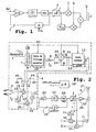
- FIG. 1 shows a transmitter, a modulation device, according to the invention.
- This modulation device comprises a regulation loop 1 essentially comprising a voltage controlled oscillator VCO whose the control input is connected, in particular via a filter of loop, at the output of a phase comparator C.
- the comparator C receives in input a Ref reference signal to be compared to a signal corresponding to output signal of the VCO oscillator.
- the frequency of signal of the oscillator is divided by a divisor by N, N being an integer but can also be a fractional size.
- Cascading with the loop 1 is present a radio transmission circuit 3, here simply represented by an antenna.
- an optional dividing circuit 2 is interposed between loop 1 and circuit 3.
- Circuit 2 modifies by division the frequency of signal delivered by the oscillator VCO of the loop 1.
- the division of divisor 2 is a division by two. This division is optional in this meaning that it is controlled by a command signal and carried out at the request, when we want the frequency of the signal emitted by the circuit 3 to be changed. For example this frequency is changed to go from one frequency in the DCS range at 1800 MHz at a frequency in the 900 MHz GSM range. By doing so, the VCO oscillator also serves good for one range than for the other. Frequency exploration of this common VCO oscillator must match the most important exploration between exploration in the higher frequency range and the double of exploration in the lower frequency range.
- the signal to be transmitted is modulated by I and Q modulation signals acting on a modulator located downstream of the divider 2, and upstream of the circuit 3.
- a modulator located downstream of the divider 2, and upstream of the circuit 3.
- filters may require the presence of filters, not shown, to interpose between the modulator and the emission circuit 3. To avoid the presence of these filters, or to use them the simplest, we can proceed differently.
- FIG. 2 shows in this respect a modulation device according to a improvement of the invention.
- This modulation device includes in cascade the regulation loop 1, optional division circuit 2 and circuit 3 radio transmission.
- the modulation device comprises a circuit 4 to modulate a reference signal admitted to the input of the Regulation loop 1.
- the signal of reference is either a REF1 reference signal or a reference signal REF2.
- the signal REF1 will be a pure sinusoidal signal at 200 KHz usable in the DCS 1800 MHz range or PCS or even UMTS while the reference signal REF2 will be a pure sinusoidal signal at a frequency of 400 KHz.
- the modulation circuit comprises a first switch 5 to choose a reference signal with a first, REF1, or a second, REF2, frequency.
- a first switch 5 to choose a reference signal with a first, REF1, or a second, REF2, frequency.
- REF1 first, REF1
- REF2 second, REF2
- Divide or not will be the same way obtained by switching.
- the division by two envisaged here is a preferred solution. Other divisions would be conceivable in relation to the divisor value of divisor 2 and in relation to the instituted channel width in each of the bands.
- the circuit of the invention has a second switch 6 for switching characteristics of modulation of a modulation signal S.
- GMSK uses a Gaussian low-pass filter upstream of a modulator of frequency.
- the circuit 4 here includes such a filter and such a modulator of frequency.
- the filter is not a priori indispensable for the invention although provides a good protection of the transmitted signal vis-à-vis the noise of the channel and better use of the properties of the decoding circuits in reception.
- the modulation signal S to be transmitted, is presented under the form of a succession of binary signals, conventionally represented by zeros and ones. In practice these signals are produced at a standardized frequency f, corresponding to 270.833 kbit / s in GSM and PCS per example. These signals are introduced into a coder 7 having a certain number of outputs related to address entries of a conversion table 8.
- the precalculated conversion table 8 performs a filtering, in particular Gaussian type filtering. Nevertheless we could do without this filtering, or this filtering could be an identity filtering.
- Table 8 is connected to a phase accumulator 9. This phase accumulator is a digital adder capable of adding a signal transmitted to a first of its inputs 10 to a signal produced by its output 11 and reintroduced on a second of its inputs 12 to the rhythm of a control signal.
- the accumulator 9 will preferably be controlled by a signal at an oversampled frequency for example 8f. Whether or not there is oversampling, the signal available at the output of the accumulator 9 serves address input to two conversion tables, respectively 13 and 14, performing the cosine and sinus transformations respectively and producing I and Q signals of known type. These I and Q signals are transformed into analog signals and are applied on first Inputs 15 and 16 of two mixers 17 and 18 respectively. Mixers 17 and 18 also receive on second inputs 19 and 20 respectively the reference signal REF1 (or REF2) and this same signal of reference out of phase by 90 °. The outputs of the mixers 17 and 18 are connected to an adder 21 whose output is used as a setpoint input of a phase comparator 22 of loop 1.
- the signal delivered by the comparator 22 is transmitted to a loop filter 23, for example, low-pass at 200 KHz.
- the signal from the filter 23 is applied as a control input to a local oscillator 24 controlled in voltage.
- the signal produced by the local oscillator is looped back to a second input of phase comparator 22 via a divider 25 by N.
- the value N is worth around 4500 or 9000 depending on the type of program chosen.
- N value jumps from one or more units according to a channel F0 or 2F0 to obtain.
- the transmission circuit 3 further comprises in a known manner a power amplifier 26 and an aerial radiation 27.
- a circuit of command 28 including a microprocessor produced on the one hand a C2F0 control signal to control the divider 25, and secondly a signal C to control switches 5 and 6.
- the frequency of the signal 2F0 is 1800 MHz.
- the switch 5 in a state, the switch 5 is placed in a position such that receives the pure sine wave REF1, at 200 KHz.
- the multiplication of loop 1 leads to output a signal at 1800 MHz (200 x 9000).
- the modulating signal is processed in a manner known in the circuits 7 to 20.
- the switch 6 corresponds to a table of 8 classic filtering.
- the circuit 28 When one wants to use the transmitter represented according to another range, by example in the GSM 900 range around 900 MHz, the circuit 28 produces a CF0 order to control the divider 25, for example by division by 4500.
- the order C is such that it switches the switches 5 and 6 and puts it by elsewhere in service the optional divider by two.
- the signal introduced in loop 1 is the signal REF2 (with modulation) either approximately in the preferred example 400 KHz.
- the loop and the multiplier N by 4500 we obtain again at the output of the oscillator 24 a signal at 1800 MHz.
- FIG. 3 will show the interest according to the invention of changing the table of filtering or, more generally, to change the modulation index of the signal modulating the reference signal.
- baseband a spectrum 29 of a signal having 200 KHz band useful.
- the diagram below shows a spectrum transposed around 2F0 (substantially 1800 MHz) whose width 31 is equal to the useful width 32 spectrum.
- the diagram just below shows that if we had used the divider by two under these conditions, the width 33 of the spectrum 34 result would be half as wide as width 31. In practice the reduction not being linear, the spectrum 34 is less broad, while not being twice less wide.
- a p (t) and A q (t) are the in-phase and quadrature components of the modulated signal.
- the value of the parameter is h or 2h. This amounts to doubling the modulation frequency.
- a particularly simple solution has been found for doubling the modulation frequency.
- phase accumulator Because of the presence of this phase accumulator, the doubling of the index of modulation that leads to the spectrum of width 36 is achieved by a doubling of the value of the modulating signal, whose frequency does not change. Alternatively one could also change the control frequency of the phase accumulator.
- FIG. 4 shows a particularly interesting example of embodiment of the encoder assembly 7, sub-tables 8 and 39 and switch 6.
- the encoder 7 is replaced by a shift register 40, for example three boxes. This ultimately leads to a Gaussian filtering preferably on a duration of three symbols of the modulating signal S admitted in the register 40.
- the S signal symbols are transmitted by the register 40 on inputs of a address decoder 41 of the table 8.
- Each addressing leads to the selection of a series 42 of recordings such as 43.
- Each record such as 43 comprises a memory word, precalculated, with a number M of bits corresponding to a precision of the desired calculation, for example 13 bits. We have not however here only represented 8-bit words for the simplification of drawing.
- a recording 44 following a previous recording 43 is read in series 42. Reading of each record is made by a transmission of the memory word read to a output register 45 having as many, M, of cells as there are bits in the memory word (43, 44 and following). At each period of the signal f, we change series 42.
- the M-1 most significant bits are taken from the register 45 and add as the most significant bit a zero weight produced by a cell 45.
- the contents of cell 46 remain unchanged at each reading 43, 44 and following. This operation divides the value by half contained in table 8.
- the same regulation loop 1 can also to serve.
- the aerial 27 is then connected via a duplexer 50 to a preamplifier 51.
- the preamplifier 51 has an output connected to two first inputs of two mixers 52 and 53 which receive on two second inputs the signal produced by the oscillator 24, in phase as well as in phase quadrature by means of a phase-shifter 54. demodulated I and Q signals. It remains to decode them to extract a signal S to which they correspond.
Landscapes
- Engineering & Computer Science (AREA)
- Signal Processing (AREA)
- Computer Networks & Wireless Communication (AREA)
- Physics & Mathematics (AREA)
- Spectroscopy & Molecular Physics (AREA)
- Microelectronics & Electronic Packaging (AREA)
- Computer Hardware Design (AREA)
- Power Engineering (AREA)
- Nonlinear Science (AREA)
- Transmitters (AREA)
- Radar Systems Or Details Thereof (AREA)
- Emergency Alarm Devices (AREA)
- Digital Transmission Methods That Use Modulated Carrier Waves (AREA)
Description
- Figure 1 : une représentation du principe de modulation d'un émetteur muni selon l'invention d'un diviseur de fréquence;
- Figure 2 : une représentation schématique du procédé et du dispositif de modulation selon l'invention ;
- Figure 3 : des diagrammes spectraux montrant respectivement la transposition de fréquences selon l'état de la technique, avec l'impossibilité évoquée, et d'autre part le perfectionnement apporté par l'invention ;
- Figure 4 : une représentation d'un exemple préféré de réalisation simple d'une partie d'un dispositif de modulation selon l'invention.
Claims (10)
- Procédé de modulation dans un émetteur émettant à la demande un signal radioélectrique dans une première ou dans une deuxième bande de fréquences, du type comportant les étapes consistant à :caractérisé en ce queproduire un signal de référence,comparer, dans un comparateur de phase (22), une phase d'un signal d'un oscillateur local (24) avec une phase du signal de référence,réguler (1) la fréquence du signal de l'oscillateur local en commandant cet oscillateur local avec un signal issu du comparateur de phase,modifier (2), à la demande (C), la fréquence ainsi régulée du signal de l'oscillateur local par division par un coefficient N avec un diviseur de fréquence pour que la fréquence corresponde à la première bande ou à la deuxième bande et on produit ainsi un signal à fréquence modifiée,
à la demande (C), le procédé comprend les étapes suivantes:les signaux de référence (REF1, REF2) et les indices de modulation étant respectivement déterminés de manière à compenser la variation de la largeur de bande dudit signal à fréquence modifiée générée par la division par le coefficient N.moduler selon un premier indice (8) de modulation un premier signal (REF1) de référence avec un signal de modulation pour servir de signal de référence, oumoduler selon un deuxième indice (39) de modulation un deuxième signal (REF2) de référence avec le signal de modulation pour servir de signal de référence, - Procédé selon la revendication 1, caractérisé en ce que, à la demande, le coefficient N est égal à deux.
- Procédé selon la revendication 1 ou 2, caractérisé par les étapes de :moduler les signaux de référence avec une chaíne de modulation comportant en cascade une table (8, 39) numérique de filtrage lue en fonction des variations (f) du signal de modulation, un accumulateur (9) de phase et un jeu de tables (13, 14) de conversion, età la demande, extraire (6) des premières valeurs ou des deuxièmes valeurs de la table de filtrage.
- Procédé selon la revendication 3, caractérisé en ce que l'étape d'extraction consiste à traiter à la demande des valeurs lues dans la table de filtrage par un décalage (46, 47).
- Procédé selon la revendication 3, caractérisé en ce que l'étape d'extraction consiste à traiter à la demande des valeurs lues dans la table de filtrage par une multiplication.
- Procédé selon la revendication 3, caractérisé en ce que l'étape d'extraction consiste à lire à la demande des valeurs dans une première (8) ou une deuxième (39) sous-table de la table de filtrage.
- Dispositif de modulation comportant en cascade une boucle (1) de régulation de fréquence munie d'un comparateur (22) de phase et un circuit (3) d'émission radioélectrique, comportant un circuit (2) de division optionnelle par un coefficient N interposé entre la boucle et le circuit d'émission,
caractérisé en ce que
le dispositif comporte un circuit (4) de modulation d'un signal de référence admis en entrée de la boucle de régulation par un signal de modulation, un premier circuit (5) de commutation pour choisir une fréquence du signal de référence entre une première (REF1) et une deuxième (REF2) fréquence, et un deuxième circuit (6) de commutation pour commuter des indices de modulation du signal de modulation,
les signaux de référence (REF1, REF2) et les indices de modulation étant respectivement déterminés de manière à compenser la variation de la largeur de bande du signal à fréquence modifiée générée par la division par le coefficient N. - Dispositif selon la revendication 7, caractérisé en ce que le circuit de division optionnelle est un circuit de division par deux.
- Dispositif selon la revendication 7 ou 8, caractérisé en ce que le deuxième circuit de commutation comporte un circuit (46, 47) de décalage de la lecture d'une table (8) de filtrage du signal de modulation.
- Dispositif selon l'une des revendications 7 à 9, caractérisé en ce que le circuit de modulation comporte deux commutateurs (48, 49) pour commuter le dispositif d'un mode d'émission à un mode de réception.
Applications Claiming Priority (2)
| Application Number | Priority Date | Filing Date | Title |
|---|---|---|---|
| FR9909535 | 1999-07-22 | ||
| FR9909535A FR2796799B1 (fr) | 1999-07-22 | 1999-07-22 | Procede et dispositif de modulation dans un emetteur |
Publications (2)
| Publication Number | Publication Date |
|---|---|
| EP1071249A1 EP1071249A1 (fr) | 2001-01-24 |
| EP1071249B1 true EP1071249B1 (fr) | 2005-12-28 |
Family
ID=9548413
Family Applications (1)
| Application Number | Title | Priority Date | Filing Date |
|---|---|---|---|
| EP00402060A Expired - Lifetime EP1071249B1 (fr) | 1999-07-22 | 2000-07-20 | Procédé et dispositif de modulation dans un émetteur |
Country Status (8)
| Country | Link |
|---|---|
| EP (1) | EP1071249B1 (fr) |
| AT (1) | ATE314771T1 (fr) |
| AU (1) | AU6578600A (fr) |
| DE (1) | DE60025086T2 (fr) |
| ES (1) | ES2255956T3 (fr) |
| FR (1) | FR2796799B1 (fr) |
| PT (1) | PT1071249E (fr) |
| WO (1) | WO2001008367A1 (fr) |
Cited By (3)
| Publication number | Priority date | Publication date | Assignee | Title |
|---|---|---|---|---|
| US7323945B2 (en) | 2004-02-10 | 2008-01-29 | Bitwave Semiconductor, Inc. | Programmable radio transceiver |
| US7508898B2 (en) | 2004-02-10 | 2009-03-24 | Bitwave Semiconductor, Inc. | Programmable radio transceiver |
| US7672645B2 (en) | 2006-06-15 | 2010-03-02 | Bitwave Semiconductor, Inc. | Programmable transmitter architecture for non-constant and constant envelope modulation |
Family Cites Families (5)
| Publication number | Priority date | Publication date | Assignee | Title |
|---|---|---|---|---|
| FI112133B (fi) * | 1996-03-29 | 2003-10-31 | Nokia Corp | Menetelmä kahdella eri taajuuusalueella toimivan radioviestinjärjestelmän suoramuunnoslähetin/vastaanottimen taajuuksien muodostamiseksi ja kahdella taajuusalueella toimivan radioviestinjärjestelmänsuoramuunnoslähetin/vastaanotin sekä edellisten käyttö matkaviestimessä |
| FI100286B (fi) * | 1996-04-01 | 1997-10-31 | Nokia Mobile Phones Ltd | Lähetin/vastaanotin RF-signaalin lähettämiseksi ja vastaanottamiseksi kahdella taajuusalueella |
| KR100224102B1 (ko) * | 1996-11-28 | 1999-10-15 | 윤종용 | 이중 대역 셀룰러 전화에 이용되는 중간주파수 선택장치 및 방법 |
| SE519263C2 (sv) * | 1996-12-02 | 2003-02-04 | Ericsson Telefon Ab L M | Anordning för sändning på flera frekvenser i ett radiokommunikationssystem |
| US5834985A (en) * | 1996-12-20 | 1998-11-10 | Telefonaktiebolaget L M Ericsson (Publ) | Digital continuous phase modulation for a DDS-driven phase locked loop |
-
1999
- 1999-07-22 FR FR9909535A patent/FR2796799B1/fr not_active Expired - Fee Related
-
2000
- 2000-07-20 AT AT00402060T patent/ATE314771T1/de not_active IP Right Cessation
- 2000-07-20 EP EP00402060A patent/EP1071249B1/fr not_active Expired - Lifetime
- 2000-07-20 DE DE60025086T patent/DE60025086T2/de not_active Expired - Lifetime
- 2000-07-20 WO PCT/FR2000/002084 patent/WO2001008367A1/fr not_active Ceased
- 2000-07-20 ES ES00402060T patent/ES2255956T3/es not_active Expired - Lifetime
- 2000-07-20 PT PT00402060T patent/PT1071249E/pt unknown
- 2000-07-20 AU AU65786/00A patent/AU6578600A/en not_active Abandoned
Cited By (5)
| Publication number | Priority date | Publication date | Assignee | Title |
|---|---|---|---|---|
| US7323945B2 (en) | 2004-02-10 | 2008-01-29 | Bitwave Semiconductor, Inc. | Programmable radio transceiver |
| US7482887B2 (en) | 2004-02-10 | 2009-01-27 | Bitwave Semiconductor, Inc. | Multi-band tunable resonant circuit |
| US7508898B2 (en) | 2004-02-10 | 2009-03-24 | Bitwave Semiconductor, Inc. | Programmable radio transceiver |
| US7580684B2 (en) | 2004-02-10 | 2009-08-25 | Bitwave Semiconductor, Inc. | Programmable radio transceiver |
| US7672645B2 (en) | 2006-06-15 | 2010-03-02 | Bitwave Semiconductor, Inc. | Programmable transmitter architecture for non-constant and constant envelope modulation |
Also Published As
| Publication number | Publication date |
|---|---|
| ATE314771T1 (de) | 2006-01-15 |
| PT1071249E (pt) | 2006-05-31 |
| WO2001008367A1 (fr) | 2001-02-01 |
| ES2255956T3 (es) | 2006-07-16 |
| EP1071249A1 (fr) | 2001-01-24 |
| FR2796799B1 (fr) | 2001-10-05 |
| AU6578600A (en) | 2001-02-13 |
| DE60025086T2 (de) | 2006-08-24 |
| DE60025086D1 (de) | 2006-02-02 |
| FR2796799A1 (fr) | 2001-01-26 |
Similar Documents
| Publication | Publication Date | Title |
|---|---|---|
| EP0624959B1 (fr) | Récepteur radio FM comprenant un circuit de suréchantillonnage | |
| EP2608401B1 (fr) | Circuit de transmission de signaux RF ASK avec adaptation des flancs des signaux de données | |
| EP1011200B1 (fr) | Circuit électronique de conversion numérique-analogique pour une chaine de transmission en bande de base | |
| FR2481549A1 (fr) | Dispositif de synthese et de demodulation combinees pour recepteurs d'ondes modulees en frequence et recepteur le comportant | |
| WO2001011783A1 (fr) | Synthetiseur de frequence a fraction n | |
| FR2949631A1 (fr) | Dispositif emission reception large bande permettant l'emission et la reception de signaux d'un canal selectionne dans une bande passante etendue dynamiquement | |
| EP1482635B1 (fr) | Chaîne d'émission réception et procédé d'émission | |
| EP1071242A1 (fr) | Dispositifs pour l'émission ou la réception de signaux cryptés par chaos déterministe et système de transmission, notamment par radiocommunications, comportant de tels dispositifs | |
| EP2266203B1 (fr) | Circuit integré et procédé de traitement d'un signal numérique multinorme à radiofréquence | |
| FR2786056A1 (fr) | Procede de reglage d'un emetteur recepteur multibande de telephonie mobile et telephone mobile ainsi obtenu | |
| FR2798790A1 (fr) | Dispositif de synthese de frequence | |
| EP1071249A1 (fr) | Procédé et dispositif de modulation dans un émetteur | |
| EP2412097B1 (fr) | Synthetiseur de frequence | |
| EP1727283A1 (fr) | Procédé et dispositif de conversion de fréquence d'échatillonnage | |
| EP1887750A1 (fr) | Dispositif de modulation par décalage de fréquence | |
| EP0649230B1 (fr) | Modulateur numérique à débit variable et son utilisation en radiodiffusion FM | |
| EP3005567B1 (fr) | Dispositif et procédé de synthèse de fréquences | |
| FR2759514A1 (fr) | Dispositif et procede numeriques de filtrage, decimation et transposition en bande de base repartie, et demodulateur numerique correspondant | |
| FR3032072A1 (fr) | Dispositif de synthese de frequence a boucle de retroaction | |
| EP0225218A1 (fr) | Procédé de synthèse de fréquence, et appareil synthétiseur utilisant ce procédé | |
| EP0948173A1 (fr) | Modulateur pour plusieurs signaux de modulation | |
| EP1303061B1 (fr) | Système de télécommunication à faible rayonnement électromagnétique non-essentiel | |
| EP1714391A2 (fr) | Procede et dispositif de conservation de signaux numeriques de formats heterogenes et son application a l'amplification numerique de signaux audio | |
| EP1071250B1 (fr) | Dispositif d'émission radioélectrique | |
| EP0369832B1 (fr) | Modulation à sauts de phase linéaires et à enveloppe constante |
Legal Events
| Date | Code | Title | Description |
|---|---|---|---|
| PUAI | Public reference made under article 153(3) epc to a published international application that has entered the european phase |
Free format text: ORIGINAL CODE: 0009012 |
|
| AK | Designated contracting states |
Kind code of ref document: A1 Designated state(s): AT BE CH CY DE DK ES FI FR GB GR IE IT LI LU MC NL PT SE |
|
| AX | Request for extension of the european patent |
Free format text: AL;LT;LV;MK;RO;SI |
|
| 17P | Request for examination filed |
Effective date: 20010724 |
|
| AKX | Designation fees paid |
Free format text: AT BE CH CY DE DK ES FI FR GB GR IE IT LI LU MC NL PT SE |
|
| 17Q | First examination report despatched |
Effective date: 20041111 |
|
| GRAP | Despatch of communication of intention to grant a patent |
Free format text: ORIGINAL CODE: EPIDOSNIGR1 |
|
| RAP1 | Party data changed (applicant data changed or rights of an application transferred) |
Owner name: TAM HOLDINGS LIMITED |
|
| RAP1 | Party data changed (applicant data changed or rights of an application transferred) |
Owner name: TCL & ALCATEL MOBILE PHONES LIMITED |
|
| GRAS | Grant fee paid |
Free format text: ORIGINAL CODE: EPIDOSNIGR3 |
|
| GRAA | (expected) grant |
Free format text: ORIGINAL CODE: 0009210 |
|
| AK | Designated contracting states |
Kind code of ref document: B1 Designated state(s): AT BE CH CY DE DK ES FI FR GB GR IE IT LI LU MC NL PT SE |
|
| PG25 | Lapsed in a contracting state [announced via postgrant information from national office to epo] |
Ref country code: AT Free format text: LAPSE BECAUSE OF FAILURE TO SUBMIT A TRANSLATION OF THE DESCRIPTION OR TO PAY THE FEE WITHIN THE PRESCRIBED TIME-LIMIT Effective date: 20051228 Ref country code: NL Free format text: LAPSE BECAUSE OF FAILURE TO SUBMIT A TRANSLATION OF THE DESCRIPTION OR TO PAY THE FEE WITHIN THE PRESCRIBED TIME-LIMIT Effective date: 20051228 |
|
| REG | Reference to a national code |
Ref country code: GB Ref legal event code: FG4D Free format text: NOT ENGLISH |
|
| REG | Reference to a national code |
Ref country code: CH Ref legal event code: EP |
|
| REG | Reference to a national code |
Ref country code: IE Ref legal event code: FG4D Free format text: LANGUAGE OF EP DOCUMENT: FRENCH |
|
| REF | Corresponds to: |
Ref document number: 60025086 Country of ref document: DE Date of ref document: 20060202 Kind code of ref document: P |
|
| GBT | Gb: translation of ep patent filed (gb section 77(6)(a)/1977) |
Effective date: 20060227 |
|
| PG25 | Lapsed in a contracting state [announced via postgrant information from national office to epo] |
Ref country code: SE Free format text: LAPSE BECAUSE OF FAILURE TO SUBMIT A TRANSLATION OF THE DESCRIPTION OR TO PAY THE FEE WITHIN THE PRESCRIBED TIME-LIMIT Effective date: 20060328 Ref country code: DK Free format text: LAPSE BECAUSE OF FAILURE TO SUBMIT A TRANSLATION OF THE DESCRIPTION OR TO PAY THE FEE WITHIN THE PRESCRIBED TIME-LIMIT Effective date: 20060328 Ref country code: GR Free format text: LAPSE BECAUSE OF FAILURE TO SUBMIT A TRANSLATION OF THE DESCRIPTION OR TO PAY THE FEE WITHIN THE PRESCRIBED TIME-LIMIT Effective date: 20060328 |
|
| REG | Reference to a national code |
Ref country code: PT Ref legal event code: SC4A Effective date: 20060315 |
|
| NLV1 | Nl: lapsed or annulled due to failure to fulfill the requirements of art. 29p and 29m of the patents act | ||
| PGFP | Annual fee paid to national office [announced via postgrant information from national office to epo] |
Ref country code: PT Payment date: 20060621 Year of fee payment: 7 |
|
| PGFP | Annual fee paid to national office [announced via postgrant information from national office to epo] |
Ref country code: CH Payment date: 20060714 Year of fee payment: 7 |
|
| REG | Reference to a national code |
Ref country code: ES Ref legal event code: FG2A Ref document number: 2255956 Country of ref document: ES Kind code of ref document: T3 |
|
| PGFP | Annual fee paid to national office [announced via postgrant information from national office to epo] |
Ref country code: IE Payment date: 20060725 Year of fee payment: 7 |
|
| PG25 | Lapsed in a contracting state [announced via postgrant information from national office to epo] |
Ref country code: MC Free format text: LAPSE BECAUSE OF NON-PAYMENT OF DUE FEES Effective date: 20060731 |
|
| PGFP | Annual fee paid to national office [announced via postgrant information from national office to epo] |
Ref country code: BE Payment date: 20060822 Year of fee payment: 7 |
|
| PLBE | No opposition filed within time limit |
Free format text: ORIGINAL CODE: 0009261 |
|
| STAA | Information on the status of an ep patent application or granted ep patent |
Free format text: STATUS: NO OPPOSITION FILED WITHIN TIME LIMIT |
|
| 26N | No opposition filed |
Effective date: 20060929 |
|
| BERE | Be: lapsed |
Owner name: *TCL & ALCATEL MOBILE PHONES LTD Effective date: 20070731 |
|
| REG | Reference to a national code |
Ref country code: PT Ref legal event code: MM4A Free format text: LAPSE DUE TO NON-PAYMENT OF FEES Effective date: 20080121 |
|
| REG | Reference to a national code |
Ref country code: CH Ref legal event code: PL |
|
| PG25 | Lapsed in a contracting state [announced via postgrant information from national office to epo] |
Ref country code: CH Free format text: LAPSE BECAUSE OF NON-PAYMENT OF DUE FEES Effective date: 20070731 Ref country code: LI Free format text: LAPSE BECAUSE OF NON-PAYMENT OF DUE FEES Effective date: 20070731 |
|
| REG | Reference to a national code |
Ref country code: IE Ref legal event code: MM4A |
|
| PG25 | Lapsed in a contracting state [announced via postgrant information from national office to epo] |
Ref country code: PT Free format text: LAPSE BECAUSE OF NON-PAYMENT OF DUE FEES Effective date: 20080121 |
|
| PG25 | Lapsed in a contracting state [announced via postgrant information from national office to epo] |
Ref country code: LU Free format text: LAPSE BECAUSE OF NON-PAYMENT OF DUE FEES Effective date: 20060720 |
|
| PG25 | Lapsed in a contracting state [announced via postgrant information from national office to epo] |
Ref country code: BE Free format text: LAPSE BECAUSE OF NON-PAYMENT OF DUE FEES Effective date: 20070731 |
|
| PG25 | Lapsed in a contracting state [announced via postgrant information from national office to epo] |
Ref country code: IE Free format text: LAPSE BECAUSE OF NON-PAYMENT OF DUE FEES Effective date: 20070720 |
|
| PG25 | Lapsed in a contracting state [announced via postgrant information from national office to epo] |
Ref country code: CY Free format text: LAPSE BECAUSE OF FAILURE TO SUBMIT A TRANSLATION OF THE DESCRIPTION OR TO PAY THE FEE WITHIN THE PRESCRIBED TIME-LIMIT Effective date: 20051228 |
|
| REG | Reference to a national code |
Ref country code: GB Ref legal event code: 732E Free format text: REGISTERED BETWEEN 20090924 AND 20090930 |
|
| REG | Reference to a national code |
Ref country code: GB Ref legal event code: 732E Free format text: REGISTERED BETWEEN 20120607 AND 20120613 |
|
| REG | Reference to a national code |
Ref country code: FR Ref legal event code: TP Owner name: Z124, GB Effective date: 20130328 Ref country code: FR Ref legal event code: CD Owner name: Z124, GB Effective date: 20130328 |
|
| REG | Reference to a national code |
Ref country code: FR Ref legal event code: PLFP Year of fee payment: 17 |
|
| PGFP | Annual fee paid to national office [announced via postgrant information from national office to epo] |
Ref country code: GB Payment date: 20160627 Year of fee payment: 17 |
|
| PGFP | Annual fee paid to national office [announced via postgrant information from national office to epo] |
Ref country code: FR Payment date: 20160622 Year of fee payment: 17 |
|
| GBPC | Gb: european patent ceased through non-payment of renewal fee |
Effective date: 20170720 |
|
| REG | Reference to a national code |
Ref country code: FR Ref legal event code: ST Effective date: 20180330 |
|
| PG25 | Lapsed in a contracting state [announced via postgrant information from national office to epo] |
Ref country code: GB Free format text: LAPSE BECAUSE OF NON-PAYMENT OF DUE FEES Effective date: 20170720 |
|
| PG25 | Lapsed in a contracting state [announced via postgrant information from national office to epo] |
Ref country code: FR Free format text: LAPSE BECAUSE OF NON-PAYMENT OF DUE FEES Effective date: 20170731 |
|
| PGFP | Annual fee paid to national office [announced via postgrant information from national office to epo] |
Ref country code: DE Payment date: 20190719 Year of fee payment: 20 Ref country code: FI Payment date: 20190722 Year of fee payment: 20 Ref country code: IT Payment date: 20190730 Year of fee payment: 20 Ref country code: ES Payment date: 20190822 Year of fee payment: 20 |
|
| REG | Reference to a national code |
Ref country code: DE Ref legal event code: R071 Ref document number: 60025086 Country of ref document: DE |
|
| REG | Reference to a national code |
Ref country code: FI Ref legal event code: MAE |
|
| REG | Reference to a national code |
Ref country code: ES Ref legal event code: FD2A Effective date: 20201029 |
|
| PG25 | Lapsed in a contracting state [announced via postgrant information from national office to epo] |
Ref country code: ES Free format text: LAPSE BECAUSE OF EXPIRATION OF PROTECTION Effective date: 20200721 |