EP1069681A2 - Switchable buffer circuit - Google Patents
Switchable buffer circuit Download PDFInfo
- Publication number
- EP1069681A2 EP1069681A2 EP00305019A EP00305019A EP1069681A2 EP 1069681 A2 EP1069681 A2 EP 1069681A2 EP 00305019 A EP00305019 A EP 00305019A EP 00305019 A EP00305019 A EP 00305019A EP 1069681 A2 EP1069681 A2 EP 1069681A2
- Authority
- EP
- European Patent Office
- Prior art keywords
- frequency
- circuit
- switching voltage
- supplied
- signal
- Prior art date
- Legal status (The legal status is an assumption and is not a legal conclusion. Google has not performed a legal analysis and makes no representation as to the accuracy of the status listed.)
- Withdrawn
Links
Images


Classifications
-
- H—ELECTRICITY
- H03—ELECTRONIC CIRCUITRY
- H03J—TUNING RESONANT CIRCUITS; SELECTING RESONANT CIRCUITS
- H03J5/00—Discontinuous tuning; Selecting predetermined frequencies; Selecting frequency bands with or without continuous tuning in one or more of the bands, e.g. push-button tuning, turret tuner
- H03J5/24—Discontinuous tuning; Selecting predetermined frequencies; Selecting frequency bands with or without continuous tuning in one or more of the bands, e.g. push-button tuning, turret tuner with a number of separate pretuned tuning circuits or separate tuning elements selectively brought into circuit, e.g. for waveband selection or for television channel selection
Definitions
- the present invention relates to a frequency-characteristic switchable buffer circuit, and particularly to a frequency-characteristic switchable buffer circuit wherein high frequency selective characteristics are respectively added to signals having selectively-supplied first and second frequencies, whereby selected frequency signal components are outputted in a state in which non-selected frequency signal components are sufficiently attenuated.
- DCS Digital Cellular System
- GSM Global System for Mobile Communications
- the DCS is a mobile communication system wherein 1805MHz through 1880MHz, 1710MHz through 1785MHz and a 1700MHz band are respectively assigned to a base-station frequency, a mobile-station frequency, and an oscillating frequency generated from a voltage-controlled oscillator (VCO) of a portable cellular phone, the number of channels to be used is 374, and GMSK (Gaussian Minimum Shift Keying) is used as a modulation scheme.
- VCO voltage-controlled oscillator
- the GSM is a mobile communication system wherein 925MHz through 960MHz, 880MHz through 915MHz and a 900MHz band are respectively assigned to a base-station frequency, a mobile-station frequency, and an oscillating frequency generated from a voltage-controlled oscillator (VCO) of a portable cellular phone, the number of channels to be used is 124, and the GMSK (Gaussian Minimum Shift Keying) is used as a modulation scheme.
- VCO voltage-controlled oscillator
- DCS and GSM are originally mobile communication systems different in system from each other
- two portable cellular phones a portable cellular phone used when mobile communications are performed by the DCS and a portable cellular phone used when mobile communications are made by the GSM, are needed to enter the two mobile communication systems of DCS and GSM.
- a portable cellular phone capable of being shared between the DCS and GSM has already been proposed wherein two voltage-controlled oscillators: a first voltage-controlled oscillator for oscillating a first frequency lying within a 1700MHz band and a second voltage-controlled oscillator for oscillating a second frequency lying within a 900MHz band, and a switching type oscillator having a switching circuit are placed within the portable cellular phone, and the switching circuit of the switching type oscillator is controlled to thereby allow the proper use of the two voltage-controlled oscillators.
- the switching circuit In the portable cellular phone capable of being shared between the DCS and GSM, when the mobile communications are performed by the DCS, the switching circuit is used to bring the first voltage-controlled oscillator to an operating state and bring the second voltage-controlled oscillator to a non-operating state, whereby an oscillating signal having a first frequency is outputted from the first voltage-controlled oscillator.
- the switching circuit when the mobile communications are carried out by the GSM, the switching circuit is used to bring the second voltage-controlled oscillator to an operating state and bring the first voltage-controlled oscillator to a non-operating state, whereby an oscillating signal having a second frequency is outputted from the second voltage-controlled oscillator.
- the oscillating signal having the first frequency or the oscillating signal having the second frequency is selected and amplified by a buffer circuit capable of performing switching between frequency characteristics, followed by supply to an available circuit.
- the frequency-characteristic switchable buffer circuit used at this time has a parallel resonance circuit (frequency selection circuit).
- the parallel resonance circuit is supplied with a first switching voltage or a second switching voltage to thereby select its characteristic selective characteristic.
- the parallel resonance circuit selects and outputs the oscillating signal having the first frequency.
- the parallel resonance circuit selects and outputs the oscillating signal having the second frequency.
- Fig. 5 is a circuit diagram showing one example of a configuration of a conventional frequency-characteristic switchable buffer circuit employed in the portable cellular phone capable of being shared between the DCS and GSM.
- the conventional frequency-characteristic switchable buffer circuit 50 has a transistor 51, a parallel resonance circuit (frequency selection circuit) 52, coupling capacitors 53 and 54, base bias resistors 55 and 56, an emitter resistor 57, a bypass capacitor 58, a one-circuit two-contacts selector switch 59, switching-voltage setting resistors 60 and 61, a bypass capacitor 62, a buffer resistor 63, a signal input terminal 64, a signal output terminal 65, and a power terminal 66.
- These circuit elements 51 through 66 are electrically connected to one another as shown in Fig. 5.
- the parallel resonance circuit 52 comprises a first inductor 52 1 , a second inductor 52 2 , a first capacitor 52 3 , a second capacitor 52 4 , a third capacitor 52 5 , and a switching diode 52 6 .
- These circuit elements 52 1 through 52 6 are electrically connected to one another as shown in Fig. 5.
- a first voltage-controlled oscillator 67 for oscillating a first frequency in this case, each of frequencies lying within a 1700MHz band
- a second voltage-controlled oscillator 68 for oscillating a second frequency in this case, each of frequencies lying within a 900MHz band
- a power supply or battery 69 a one-circuit two-contacts selector switch 70 are placed on the preceding stage side of the frequency-characteristic switchable buffer circuit 50.
- These circuit elements 67 through 70 are electrically connected to one another as shown in Fig. 5.
- the selector switch 59 and the selector switch 70 are selected or changed in interlock with each other by a control signal to be described later.
- the conventional frequency-characteristic switchable buffer circuit 50 having the above-described configuration is operated as follows:
- movable contacts of the selector switch 59 and the selector switch 70 are respectively changed over from positions indicated by solid lines shown in Fig. 5 to positions indicated by dotted lines illustrated in Fig. 5 according to a first control signal outputted from a controller (not shown).
- the first voltage-controlled oscillator 67 is electrically connected to the power supply 69 so that it is brought to an operating state.
- a signal having a first frequency (corresponding to any of the frequencies lying within the 1700MHz band) is outputted from the first voltage-controlled oscillator 67.
- the second voltage-controlled oscillator 68 is electrically disconnected from the power supply 69 so that it is brought to a non-operating state. Owing to the changeover of the movable contact of the selector switch 59 to the position indicated by the dotted line, a first switching voltage corresponding to a positive voltage is supplied to the parallel resonance circuit 52 so that the parallel resonance circuit 52 parallel-resonates at the first frequency (corresponding to any of the frequencies lying within the 1700MHz band) as will be described below.
- the signal having the first frequency (corresponding to any of the frequencies lying within the 1700MHz band) outputted from the first voltage-controlled oscillator 67 is supplied to the signal input terminal 64 at this time, only the signal having the first frequency (corresponding to any of the frequencies lying within the 1700MHz band) is selected and amplified by the parallel resonance circuit 52 which is electrically connected as a load of the transistor 51 and resonates in parallel at the first frequency (corresponding to any of the frequencies lying within the 1700MHz band), when the signal is amplified by the common emitter-connected transistor 51. Afterwards, the amplified signal having the first frequency (corresponding to any of the frequencies lying within the 1700MHz band) is supplied to an available circuit through the signal output terminal 65.
- the movable contacts of the selector switch 59 and the selector switch 70 are respectively changed over to the positions indicated by the solid lines shown in Fig. 5 according to a second control signal outputted from the controller in the same manner as described above.
- the second voltage-controlled oscillator 68 is electrically connected to the power supply 69 so that it is brought to an operating state.
- a signal having a second frequency (any of frequencies lying within a 900MHz band) is outputted from the second voltage-controlled oscillator 68.
- the first voltage-controlled oscillator 67 is electrically disconnected from the power supply 69 so that it is brought to a non-operating state. Owing to the changeover of the movable contact of the selector switch 59 to the position indicated by the solid line, a second switching voltage corresponding to a ground voltage is supplied to the parallel resonance circuit 52 so that the parallel resonance circuit 52 parallel-resonates at the second frequency (corresponding to any of the frequencies lying within the 900MHz band) as will be described below.
- the signal having the second frequency (corresponding to any of the frequencies lying within the 900MHz band) outputted from the second voltage-controlled oscillator 68 is supplied to the signal input terminal 64, only the signal having the second frequency (corresponding to any of the frequencies lying within the 900MHz band) is selected and amplified by the parallel resonance circuit 52 which is electrically connected as the load of the transistor 51 and resonates in parallel at the second frequency (corresponding to any of the frequencies lying within the 900MHz band), when the outputted signal is amplified by the common emitter-connected transistor 51. Afterwards, the amplified signal having the second frequency (corresponding to any of the frequencies lying within the 900MHz band) is supplied to the available circuit through the signal output terminal 65.
- the second switching voltage corresponding to the ground voltage is first supplied to the parallel resonance circuit 52 to cause the parallel resonance circuit 52 to parallel-resonate at the signal having the second frequency (corresponding to any of the frequencies lying within the 900MHz band)
- the second switching signal voltage corresponding to the ground voltage is supplied to the parallel resonance circuit 52.
- the switching diode 52 6 is turned off so that a point where the second capacitor 52 4 and the third capacitor 52 5 are connected to each other, is brought to a state of being separated from a ground point.
- a parallel resonance frequency approximately equal to the second frequency (corresponding to any of the frequencies lying within the 900MHz band) is set to the parallel resonance circuit 52 by a first parallel-connected circuit comprising the first inductor 52 1 .
- the parallel resonance circuit 52 can be easily set to the second frequency (corresponding to any of the frequencies lying within the 900MHz band).
- the first switching signal corresponding to the positive voltage is supplied to the parallel resonance circuit 52 to thereby allow the parallel resonance circuit 52 to parallel-resonate at the signal having the first frequency (corresponding to any of the frequencies lying within the 1700MHz band)
- the first switching signal corresponding to the positive voltage is supplied to the parallel resonance circuit 52.
- the switching diode 52 6 is turned on so that the connecting point provided between the second capacitor 52 4 and the third capacitor 52 5 is brought to a state of being connected to the ground point.
- a parallel resonance frequency approximately equal to the first frequency (corresponding to any of the frequencies lying within the 1700MHz band) is set to the parallel resonance circuit 52 by the second inductor 52 2 , the second capacitor 52 4 electrically parallel-connected thereto, and the third capacitor 52 5 .
- the parallel-connected circuit comprising the second capacitor 52 4 and the third capacitor 52 5 indicates an integrated capacitor, and the parallel resonance circuit 52 results in an equivalent circuit comprising the second inductor 52 2 and integrated capacitor connected in parallel.
- the parallel resonance frequency of the parallel resonance circuit 52 can be easily set to the first frequency (corresponding to any of the frequencies lying within the 1700MHz band).
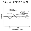
- Fig. 6 is a characteristic diagram showing one example of a gain vs. frequency characteristic obtained in the conventional frequency-characteristic switchable buffer circuit 50 shown in Fig. 5.
- the horizontal axis indicates a frequency (whose unit is represented in GHz), and the vertical axis indicates gain (dB).
- a curve (indicated by a solid line) a is a characteristic obtained when the buffer circuit 50 parallel-resonates at the first frequency lying in the 1.7MHz band (1700MHz band).
- a curve (indicated by a dotted line) b is a characteristic obtained when the buffer circuit 50 is tuned to the second frequency lying in the 0.9GHz (900MHz band).
- the conventional frequency-characteristic switchable buffer circuit 50 can take out a signal of a first frequency having large signal amplitude because the gain thereof with respect to the signal having the first frequency is large, when the signal having the first frequency (corresponding to any of frequencies lying within a 1700MHz band) is selected as an amplifying signal.
- the frequency-characteristic switchable buffer circuit 50 can take out the signal of the second frequency having large signal amplitude in the same manner as described above since the gain thereof with respect to the second frequency is large.
- the conventional frequency-characteristic switchable buffer circuit 50 does not obtain attenuation with respect to a signal on the side of a frequency higher than the first frequency in a large way so much when the signal having the first frequency (corresponding to any of the frequencies lying within the 1700MHz band) is selected, the rate of the output of a signal having a spurious frequency relative to the first frequency simultaneously with the signal having the first frequency becomes high. Further, since attenuation of harmonic components of the signal having the second frequency is not obtained in a large way so much when the signal having the second frequency (corresponding to any of the frequencies lying within the 900MHz band) is selected, the rate of the output of a signal having a spurious frequency simultaneously with the signal having the second frequency increases.
- a frequency-characteristic switchable buffer circuit which comprises an amplifying stage, a parallel resonance circuit which serves as an output load of the amplifying stage, a frequency trap circuit connected between an input of the amplifying stage and a reference potential point, and a frequency switching voltage generator for selectively generating a first switching voltage or a second switching voltage, and wherein the parallel resonance circuit parallel-resonates at a first frequency when the first switching voltage is supplied thereto and parallel-resonates at a second frequency different from the first frequency when the second switching voltage is supplied thereto, and the frequency trap circuit comprises a series circuit comprised of a diode and a capacitor, and series-resonates at the second frequency when the first switching voltage is supplied thereto and series-resonates at the first frequency when the second switching voltage is supplied thereto.
- a first frequency is supplied from a first oscillator
- a second frequency is supplied from a second oscillator and the first oscillator and second oscillator are alternately changed to an operating or non-operating state
- a frequency switching voltage generator is switched so as to output a first switching voltage
- the frequency switching voltage generator is switched so as to output a second switching voltage
- a second frequency and a first frequency have a relationship between a fundamental wave frequency and a harmonic frequency thereof, the second frequency is directly supplied from an oscillator and the first frequency is supplied from a harmonic generator to which the second frequency is applied, and when the first frequency is supplied from the oscillator, a frequency switching voltage generator is changed so as to output a first switching voltage and when the second frequency is supplied from the harmonic generator, the frequency switching voltage generator is changed so as to output a second switching voltage.
- the first switching voltage when a first switching voltage is supplied to a parallel resonance circuit to allow the parallel resonance circuit to parallel-resonate at a first frequency, thereby selecting and outputting a signal having the first frequency, the first switching voltage is supplied even to a frequency trap circuit to thereby cause the frequency trap circuit to series-resonate at a frequency lower than the first frequency.
- a trap is developed on the side of a frequency higher than the first frequency by its bound or bounce. The developed trap serves so as to attenuate signal components of a spurious frequency of the signal having the first frequency.
- the second switching voltage is supplied even to the frequency trap circuit to thereby allow the frequency trap circuit to series-resonate at a frequency in the neighborhood of 1700MHz, thereby serving so as to attenuate signal components of a spurious frequency of the second frequency.
- the signal having the first frequency is selected, attenuation of signal components of a spurious frequency in the signal having the first frequency can be increased.
- the signal having the second frequency when the signal having the second frequency is selected, attenuation of a signal having a spurious frequency included in the signal having the second frequency can be increased, whereby the signal having the first frequency or the signal having the second frequency can be selected and outputted in a state in which the spurious signal components are little included therein.
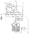
- Fig. 1 is a circuit configurational diagram showing a first embodiment of a frequency-characteristic switchable buffer circuit according to the present invention and shows an example in which the present buffer circuit is used in a portable cellular phone which can be shared between the DCS and GSM.
- the frequency-characteristic switchable buffer circuit comprises a transistor 2, a parallel resonance circuit (frequency selection circuit) 3, coupling capacitors 4 and 5, a frequency trap circuit 6, base bias resistors 7 and 8, an emitter resistor 9, a bypass capacitor 10, a one-circuit two-contacts selector switch 11, switching-voltage setting resistors 12 and 13, a bypass capacitor 14, buffer resistors 15 and 16, a signal input terminal 17, a signal output terminal 18, and a power terminal 19.
- These circuit elements 1 through 19 are electrically connected to one another as shown in Fig. 1.
- the parallel resonance circuit 3 includes a first inductor 3 1 , a second inductor 3 2 , a first capacitor 3 3 , a second capacitor 3 4 , a third capacitor3 5 , and a first switching diode 3 6 .
- the frequency trap circuit 6 has a sixth capacitor 6 1 , and a second switching diode 6 2 . These circuit elements 3 1 through 3 6 and 6 1 and 6 2 are electrically connected to one another as shown in Fig. 1.
- the inductance of the first inductor 3 1 is selected so as to be larger than that of the second inductor 3 2
- the capacitance of the third capacitor 3 5 is selected so as to be much larger than that of the second capacitor 3 4 .
- the capacitance of the third capacitor 3 5 is 1000pF
- the capacitance of the second capacitor 3 4 is selected so as to take or assume about 2pF.
- a first voltage-controlled oscillator 20 for oscillating a first frequency in this case, frequencies lying within a 1700MHz band
- a second voltage-controlled oscillator 21 for oscillating a second frequency in this case, frequencies lying within a 900MHz band
- a power supply or battery 2 and a one-circuit two-contacts selector switch 23 are placed on the preceding stage side of the frequency-characteristic switchable buffer circuit 1.
- These circuit elements 20 through 23 are electrically connected to one another as shown in Fig. 1. In this case, the selector switch 11 and the selector switch 23 are selected or changed in interlock with a control signal to be described later.
- the frequency-characteristic switchable buffer circuit 1 (hereinafter called “buffer circuit 1 according to the present embodiment") and the conventional frequency-characteristic switchable buffer circuit 50 (hereinafter called “conventional buffer circuit 50") shown in Fig. 5 are different in configuration from each other only in that the buffer circuit 1 according to the present embodiment is equipped with the frequency trap circuit 6, and a first switching voltage or a second switching voltage is selectively supplied to the second switching diode 6 2 of the frequency trap circuit 6 in association with the provision of the frequency trap circuit 6, whereas the conventional buffer circuit 50 is not equipped with such a frequency trap circuit 6. There is no difference between the buffer circuit 1 according to the present embodiment and the conventional buffer circuit 50 in other configurations.
- the parallel resonance circuit 3 employed in the buffer circuit 1 according to the present embodiment is identical in configuration to the parallel resonance circuit 52 employed in the conventional buffer circuit 50, the operation of the buffer circuit 1 according to the present embodiment at the time that either the first switching voltage or the second switching voltage is supplied to the parallel resonance circuit 3 thereof, is identical to that of the already-described conventional buffer circuit 50 at the time that either the first switching voltage or the second switching voltage is supplied to the parallel resonance circuit 52 thereof.
- the operation of the conventional buffer circuit 50 at the time that the first switching voltage or the second switching voltage is supplied to the parallel resonance circuit 52 thereof is quoted for the following description of the operation of the buffer circuit 1 according to the present embodiment.
- a description made of the operation of the buffer circuit 1 according to the present embodiment at the time that the first switching voltage or the second switching voltage is supplied to the parallel resonance circuit 3 thereof, will be omitted.
- the frequency-characteristic switchable buffer circuit according to the first embodiment, having the above-described configuration is operated as follows:
- movable contacts of the selector switch 11 and the selector switch 23 are respectively changed over from positions indicated by solid lines shown in Fig. 1 to positions indicated by dotted lines illustrated in Fig. 1 according to a first control signal outputted from a controller (not shown).
- a controller not shown
- the first voltage-controlled oscillator 20 is electrically connected to the power supply 22 so that it is brought to an operating state.
- a signal having a first frequency (corresponding to any of frequencies lying within the 1700MHz band) is outputted from the first voltage-controlled oscillator 20.
- the second voltage-controlled oscillator 21 is electrically disconnected from the power supply 22 so that it is brought to a non-operating state.
- a first switching voltage corresponding to a positive voltage is supplied to the parallel resonance circuit 3 so that the parallel resonance circuit 3 parallel-resonates at the first frequency (corresponding to any of frequencies lying within the 1700MHz band) as already described above.
- the first switching voltage corresponding to the positive voltage is supplied to the frequency trap circuit 6 so that the frequency trap circuit 6 series-resonates at a second frequency (corresponding to any of frequencies lying within the 900MHz band) as will be described below.
- the signal having the first frequency (corresponding to any of the frequencies lying within the 1700MHz band) outputted from the first voltage-controlled oscillator 20 is supplied to the signal input terminal 17, only the signal having the first frequency (corresponding to any of the frequencies lying within the 1700MHz band) is selected and amplified by the parallel resonance circuit 3 which is electrically connected as a collector load of the transistor 2 and resonates in parallel at the first frequency (corresponding to any of the frequencies lying within the 1700MHz band), when the signal is amplified by the common emitter-connected transistor 2. Afterwards, the amplified signal having the first frequency (corresponding to any of the frequencies lying within the 1700MHz band) is supplied to an available circuit through the signal output terminal 18.
- the frequency trap circuit 6 which resonates in series at a frequency lower than the first frequency, is electrically connected between the base of the transistor 2 and the ground.
- the frequency trap circuit 6 is caused to resonate in series at the low frequency, a bounce or bound trap thereof occurs on the higher frequency side of the first frequency and thereby signal components of a spurious frequency contained in the signal having the first frequency are sufficiently attenuated by the trap. It is therefore possible to supply only the signal having the first frequency, which does not include the signal components of the spurious frequency, to the signal output terminal 18.
- the movable contacts of the selector switch 11 and the selector switch 23 are respectively changed over to the positions indicated by the solid lines shown in Fig. 1 according to a second control signal outputted from the controller in the same manner as described above.
- the second voltage-controlled oscillator 21 is electrically connected to the power supply 22 so that it is brought to an operating state.
- a signal having a second frequency (any of frequencies lying within a 900MHz band) is outputted from the second voltage-controlled oscillator 21.
- the first voltage-controlled oscillator 20 is electrically disconnected from the power supply 22 so that it is brought to a non-operating state.
- a second switching voltage corresponding to a ground voltage is supplied to the parallel resonance circuit 3 so that the parallel resonance circuit 3 parallel-resonates at the second frequency (corresponding to any of the frequencies lying within the 900MHz band) as already described above.
- the second switching voltage corresponding to the ground voltage is supplied to the frequency trap circuit 6 so that the frequency trap circuit 6 series-resonates at each frequency lying within the 1700MHz band as will be described below.
- the signal having the second frequency (corresponding to any of the frequencies lying within the 900MHz band) outputted from the second voltage-controlled oscillator 21 is supplied to the signal input terminal 17, only the signal having the second frequency (corresponding to any of the frequencies lying within the 900MHz band) is selected and amplified by the parallel resonance circuit 3 which is electrically connected as the collector load of the transistor 2 and resonates in parallel at the second frequency (corresponding to any of the frequencies lying within the 900MHz band), when the outputted signal is amplified by the common emitter-connected transistor 2. Afterwards, the amplified signal having the second frequency (corresponding to any of the frequencies lying within the 900MHz band) is supplied to the available circuit through the signal output terminal 18.
- the frequency trap circuit 6, which resonates in series at each frequency lying within the 1700MHz band, is electrically connected between the base of the transistor 2 and the ground, and hence spurious signal components contained in the signal having the second frequency are sufficiently attenuated by the frequency trap circuit 6. It is therefore possible to supply only the signal having the second frequency, which does not include the spurious signal components, to the signal output terminal 18.
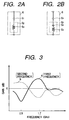
- Figs. 2A and 2B are respectively equivalent circuit diagrams of the frequency trap circuit 6 shown in Fig. 1 to which either a first switching signal or a second switching signal is supplied.
- a second switching diode 6 2 When a first switching voltage corresponding to a positive voltage is supplied to a frequency trap circuit 6, a second switching diode 6 2 is first turned on so that only a lead inductor 6 3 of a lead thereof, which is constituted as the second switching diode 6 2 , remains as a circuit element and is electrically series-connected to a fourth capacitor 6 1 .
- the frequency trap circuit 6 results in a series circuit comprising the fourth capacitor 6 1 and the lead inductor 6 3 as shown in Fig. 2A.
- the second switching diode 6 2 is turned off so that a series circuit comprising a lead inductor 6 3 of a lead thereof and a junction capacitance 6 4 of a semiconductor junction thereof, which are constituted as the second switching diode 6 2 , remains as a circuit element and is electrically series-connected to a fourth capacitor 6 1 .
- the frequency trap circuit 6 results in a series circuit comprising the fourth capacitor 6 1 , the lead inductor 6 3 and the junction capacitance 6 4 as shown in Fig. 2B.
- the capacitance value of the fourth capacitor 6 1 , the inductance value of the lead inductor 6 3 and the capacitance value of the junction capacitance 6 4 are respectively selected to thereby allow the series circuit to resonate in series at each frequency lying within the 1700MHz band, whereby spurious high-frequency signal components of the second frequency can be greatly attenuated.
- Fig. 3 is a characteristic diagram showing a gain vs. frequency characteristic obtained in the frequency-characteristic switchable buffer circuit 1 according to the present embodiment shown in Fig. 1.
- the horizontal axis indicates a frequency (whose unit is represented in GHz), and the vertical axis indicates gain (dB).
- a curve (indicated by a solid line) a is a characteristic obtained when the buffer circuit 1 parallel-resonates at the first frequency lying in the 1.7MHz band (1700MHz band) and the bounce or bound trap is developed on the side of the frequency higher than the first frequency by the frequency trap circuit 6.
- a curve (indicated by a dotted line) b is a characteristic obtained when the buffer circuit 1 resonates in parallel at the second frequency lying in the 0.9GHz band (900MHz band) and the frequency trap circuit 6 resonates in series at the 1.7MHz band (1700MHz band).
- the gain of the buffer circuit 1 with respect to the first frequency increases and attenuation of a spurious signal on the side of the frequency higher than the first frequency also increases greatly, as shown in the curves a and b of Fig. 3.
- the frequency-characteristic switchable buffer circuit 1 can not only greatly increase the attenuation of signal components of the spurious frequency of the first frequency when the signal having the first frequency (corresponding to any of the frequencies lying within the 1700MHz band) is selected, but also greatly increase the attenuation of signal components of the frequency lying within the 1700MHz band even when the signal having the second frequency (corresponding to any of the frequencies lying within the 900MHz band) is selected, thus making it possible to select and output the signal having the second frequency in a state in which the spurious signal components are little included therein.
- the first embodiment has been described by the example in which the frequency-characteristic switchable buffer circuit 1 is used in the portable cellular phone capable of being shared between the DCS and GSM, and the frequency of the oscillating signal outputted from the first voltage-controlled oscillator 20 is any of the frequencies lying within the 1700MHz band and the frequency of the oscillating signal outputted from the second voltage-controlled oscillator 21 is any of the frequencies lying within the 900MHz band.
- the frequency-characteristic switchable buffer circuit 1 according to the present invention is not limited to the case in which it is used in the above-described portable cellular phone. It may be used in other similar apparatuses.
- the respective oscillating frequencies of the first voltage-controlled oscillator 20 and the second voltage-controlled oscillator 21 are not limited to those lying within the aforementioned frequency bands. If ones whose oscillating frequency bands are appropriately separated from each other, are adopted, then other frequency bands may be used.
- the two oscillators according to the present invention are not necessarily limited to the voltage-controlled oscillators.
- An oscillator circuit for generating oscillating signals lying within a fixed frequency band may be used.
- Fig. 4 is a circuit configurational diagram showing a second embodiment of a frequency-characteristic switchable buffer circuit according to the present invention and illustrates a configurational example in which a second frequency and a first frequency satisfy a fundamental wave frequency and a secondary harmonic frequency thereof.
- the frequency-characteristic switchable buffer circuit 1 according to the second embodiment is identical in configuration to the frequency-characteristic switchable buffer circuit 1 according to the first embodiment.
- a configuration on the preceding side of the frequency-characteristic switchable buffer circuit 1 according to the second embodiment includes a single voltage-controlled oscillator 24, a second harmonic generator 25, an interlock selector switch 26 comprising two pairs of one-circuit two-contacts selector switches 26 1 and 26 2 , and a power supply or battery 22.
- the present configuration is different from the configuration on the preceding side of the frequency-characteristic switchable buffer circuit 1 according to the first embodiment, which is provided with the first voltage-controlled oscillator 20 and the second voltage-controlled oscillator 21.
- the power supply 22 is electrically disconnected from the second harmonic generator 25 by the selector switch 26 2 . Therefore, the power supply 22 is electrically connected to the voltage-controlled oscillator 24 alone, so that the fundamental wave frequency, e.g., an oscillating signal having a second frequency lying within a 900MHz band is outputted from the voltage-controlled oscillator 24.
- the oscillating signal is supplied to a signal input terminal 17 of the frequency-characteristic switchable buffer circuit 1 through the selector switch 26 1 .
- the power supply 22 is electrically connected even to the second harmonic generator 25 by the selector switch 26 2 , so that the second harmonic generator 25 is brought to an operating state.
- the second harmonic generator 25 outputs a secondary harmonic of the fundamental wave frequency supplied from the voltage-controlled oscillator 24, e.g., an oscillating signal having a first frequency lying within a 1700MHz band in response to the fundamental wave frequency, e. g., the oscillating signal having the second frequency lying within the 900MHz band.
- the oscillating signal is supplied to the signal input terminal 17 of the frequency-characteristic switchable buffer circuit 1 through the selector switch 26 1 .
- the operation of the frequency-characteristic switchable buffer circuit 1 according to the second embodiment at the time that the oscillating signal having the second frequency lying within the 900MHz band is supplied to the signal input terminal 17, is the same as that of the frequency-characteristic switchable buffer 1 according to the first embodiment at the time that the oscillating signal having the second frequency lying within the 900MHz band is supplied to the signal input terminal 17.
- the frequency-characteristic switchable buffer circuit 1 can also not only greatly increase attenuation of signal components of a spurious frequency with respect to the first frequency when the signal having the first frequency (corresponding to any of frequencies lying within the 1700MHz band) is selected, but also greatly increase attenuation of signal components of any of frequencies lying within the 1700MHz band, which is a spurious frequency of the signal having the second frequency even when the signal having the second frequency (corresponding to any of frequencies lying within the 900MHz band) is selected, thus making it possible to select and output the signal having the first frequency or the signal having the second frequency in a state in which the spurious signal components are little included therein.
- the single oscillator employed in the present invention is not limited to the voltage-controlled oscillator. It may be a single oscillator which generates each of oscillating signals in a fixed frequency band.
- the first switching voltage when a first switching voltage is supplied to a parallel resonance circuit to allow the parallel resonance circuit to parallel-resonate at a first frequency, thereby selecting and outputting a signal having the first frequency, the first switching voltage is supplied even to a frequency trap circuit to thereby cause the frequency trap circuit to series-resonate at a frequency lower than the first frequency.
- a trap is developed on the side of a frequency higher than the first frequency by its bound or bounce. The developed trap attenuates signal components of a spurious frequency higher than the first frequency.
- the second switching voltage is supplied even to the frequency trap circuit to thereby allow the frequency trap circuit to series-resonate at any of frequencies lying within a 1700MHz band, whereby signal components of any of the frequencies lying within the 1700MHz band, which is a spurious frequency with respect to the second frequency, are attenuated. Therefore, when the signal having the second frequency is selected, attenuation of the spurious signal components thereof can be increased. From the above result, an effect is brought about in that the signal having the first frequency or the signal having the second frequency can be selected and outputted in a state in which it little includes the spurious signal components.
Landscapes
- Inductance-Capacitance Distribution Constants And Capacitance-Resistance Oscillators (AREA)
- Amplifiers (AREA)
- Transmitters (AREA)
- Electronic Switches (AREA)
Abstract
Description
Claims (6)
- A frequency-characteristic switchable buffer circuit, comprising:an amplifying stage;a parallel resonance circuit which serves as an output load of the amplifying stage;a frequency trap circuit connected between an input of the amplifying stage and a reference potential point; anda frequency switching voltage generator for selectively generating a first switching voltage or a second switching voltage; and
wherein the parallel resonance circuit parallel-resonates at a first frequency when the first switching voltage is supplied thereto and parallel-resonates at a second frequency different from the first frequency when the second switching voltage is supplied thereto, andthe frequency trap circuit comprises a series circuit comprised of a diode and a capacitor, and series-resonates at the second frequency when the first switching voltage is supplied thereto and series-resonates at the first frequency when the second switching voltage is supplied thereto. - The frequency-characteristic switchable buffer circuit as claimed in claim 1, wherein the first frequency is supplied from a first oscillator, the second frequency is supplied from a second oscillator and the first oscillator and second oscillator are alternately changed to an operating or non-operating state, and when the first oscillator is in the operating state, the frequency switching voltage generator is switched so as to output the first switching voltage and when the second oscillator is in the operating state, the frequency switching voltage generator is switched so as to output the second switching voltage.
- The frequency-characteristic switchable buffer circuit as claimed in claim 2, wherein the first oscillator and the second oscillator are respectively voltage-controlled oscillators.
- The frequency-characteristic switchable buffer circuit as claimed in claim 2 or 3, wherein the first oscillator outputs an oscillating signal having a first frequency lying within a 1700MHz band employed in a DCS mobile communication, and the second oscillator outputs an oscillating signal having a second frequency lying within a 900MHz band employed in a GSM mobile communication.
- The frequency-characteristic switchable buffer circuit as claimed in any preceding claim, wherein the second frequency and the first frequency have a relationship between a fundamental wave frequency and a harmonic frequency thereof, the second frequency is directly supplied from an oscillator and the first frequency is supplied from a harmonic generator to which the second frequency is applied, and when the first frequency is supplied from the oscillator, the frequency switching voltage generator is changed so as to output the first switching voltage and when the second frequency is supplied from the harmonic generator, the frequency switching voltage generator is changed so as to output the second switching voltage.
- The frequency-characteristic switchable buffer circuit as claimed in claim 5, wherein-the oscillator is a voltage-controlled oscillator.
Applications Claiming Priority (2)
| Application Number | Priority Date | Filing Date | Title |
|---|---|---|---|
| JP19800499 | 1999-07-12 | ||
| JP19800499 | 1999-07-12 |
Publications (2)
| Publication Number | Publication Date |
|---|---|
| EP1069681A2 true EP1069681A2 (en) | 2001-01-17 |
| EP1069681A3 EP1069681A3 (en) | 2003-08-13 |
Family
ID=16383920
Family Applications (1)
| Application Number | Title | Priority Date | Filing Date |
|---|---|---|---|
| EP00305019A Withdrawn EP1069681A3 (en) | 1999-07-12 | 2000-06-14 | Switchable buffer circuit |
Country Status (2)
| Country | Link |
|---|---|
| US (1) | US6380813B1 (en) |
| EP (1) | EP1069681A3 (en) |
Families Citing this family (3)
| Publication number | Priority date | Publication date | Assignee | Title |
|---|---|---|---|---|
| JP4206035B2 (en) * | 2003-12-08 | 2009-01-07 | アルプス電気株式会社 | Voltage controlled oscillator |
| CA2624720C (en) * | 2005-10-14 | 2015-12-22 | Carrier Web Llc | System and method for real-time management of mobile resources |
| US7577002B2 (en) * | 2005-12-08 | 2009-08-18 | System General Corp. | Frequency hopping control circuit for reducing EMI of power supplies |
Family Cites Families (4)
| Publication number | Priority date | Publication date | Assignee | Title |
|---|---|---|---|---|
| DE1286081B (en) * | 1964-07-08 | 1969-01-02 | Telefunken Patent | High frequency amplifier with a transistor |
| JPH09298477A (en) * | 1995-06-29 | 1997-11-18 | Sony Corp | Shortwave receiver and lowpass filter |
| JPH09307365A (en) | 1996-05-15 | 1997-11-28 | Alps Electric Co Ltd | Amplifier and portable telephone set using the amplifier |
| JPH10163750A (en) * | 1996-11-27 | 1998-06-19 | Tdk Corp | Voltage control oscillator |
-
2000
- 2000-06-14 EP EP00305019A patent/EP1069681A3/en not_active Withdrawn
- 2000-07-11 US US09/613,893 patent/US6380813B1/en not_active Expired - Fee Related
Also Published As
| Publication number | Publication date |
|---|---|
| EP1069681A3 (en) | 2003-08-13 |
| US6380813B1 (en) | 2002-04-30 |
Similar Documents
| Publication | Publication Date | Title |
|---|---|---|
| JP3643259B2 (en) | High frequency tuning amplifier for buffer | |
| JP2004040810A (en) | Method and apparatus for receiving multi-band radio frequency in mobile communication system | |
| WO2017204347A1 (en) | High-frequency filter device and communication device | |
| US3903487A (en) | Multi-circuit selection filter for two different frequency ranges | |
| JP3944410B2 (en) | Television tuner input circuit | |
| EP1087519B1 (en) | Switch-type oscillating circuit for providing isolation between first and second oscillating circuits | |
| EP1069681A2 (en) | Switchable buffer circuit | |
| US6876401B2 (en) | FM-broadcast-receivable television tuner for preventing adjacent-channel interference | |
| JP3848512B2 (en) | Buffer circuit with switchable frequency characteristics | |
| US7088984B2 (en) | Electronic tuner | |
| KR20010007383A (en) | Switch type oscillation circuit | |
| US5170498A (en) | Band switching filter and satellite broadcast receiving system using the same | |
| JP3614614B2 (en) | Television signal receiving tuner | |
| JP4389358B2 (en) | High frequency communication equipment | |
| EP2091151A1 (en) | Television tuner | |
| KR20020084776A (en) | Voltage controlled oscillator for multi-band | |
| JP3103017U (en) | Television tuner | |
| EP0765044A2 (en) | A radiotelephone operating in a time-divided radiotelephone system | |
| US7190414B2 (en) | Input circuit of television tuner in which interference caused by FM broadcasting signal is attenuated | |
| JP3677396B2 (en) | High frequency circuit | |
| JPS6338589Y2 (en) | ||
| JP2003258675A (en) | Communication control method | |
| KR980012870A (en) | Television tuner circuit | |
| KR20050012914A (en) | Triple band TX/RX multiplex VCO for TDMA type mobile wireless device | |
| JPH0380615A (en) | Electronic tuner input circuit |
Legal Events
| Date | Code | Title | Description |
|---|---|---|---|
| PUAI | Public reference made under article 153(3) epc to a published international application that has entered the european phase |
Free format text: ORIGINAL CODE: 0009012 |
|
| AK | Designated contracting states |
Kind code of ref document: A2 Designated state(s): AT BE CH CY DE DK ES FI FR GB GR IE IT LI LU MC NL PT SE |
|
| AX | Request for extension of the european patent |
Free format text: AL;LT;LV;MK;RO;SI |
|
| PUAL | Search report despatched |
Free format text: ORIGINAL CODE: 0009013 |
|
| AK | Designated contracting states |
Designated state(s): AT BE CH CY DE DK ES FI FR GB GR IE IT LI LU MC NL PT SE |
|
| AX | Request for extension of the european patent |
Extension state: AL LT LV MK RO SI |
|
| RIC1 | Information provided on ipc code assigned before grant |
Ipc: 7H 03F 3/191 B Ipc: 7H 03J 5/24 A |
|
| 17P | Request for examination filed |
Effective date: 20030807 |
|
| AKX | Designation fees paid |
Designated state(s): DE FR |
|
| STAA | Information on the status of an ep patent application or granted ep patent |
Free format text: STATUS: THE APPLICATION IS DEEMED TO BE WITHDRAWN |
|
| 18D | Application deemed to be withdrawn |
Effective date: 20070103 |