EP1069606A2 - Method for fabricating a semiconductor structure with reduced leakage current destiny - Google Patents
Method for fabricating a semiconductor structure with reduced leakage current destiny Download PDFInfo
- Publication number
- EP1069606A2 EP1069606A2 EP00115127A EP00115127A EP1069606A2 EP 1069606 A2 EP1069606 A2 EP 1069606A2 EP 00115127 A EP00115127 A EP 00115127A EP 00115127 A EP00115127 A EP 00115127A EP 1069606 A2 EP1069606 A2 EP 1069606A2
- Authority
- EP
- European Patent Office
- Prior art keywords
- forming
- fabricating
- semiconductor structure
- layer
- buffer layer
- Prior art date
- Legal status (The legal status is an assumption and is not a legal conclusion. Google has not performed a legal analysis and makes no representation as to the accuracy of the status listed.)
- Withdrawn
Links
Images

Classifications
-
- H—ELECTRICITY
- H10—SEMICONDUCTOR DEVICES; ELECTRIC SOLID-STATE DEVICES NOT OTHERWISE PROVIDED FOR
- H10D—INORGANIC ELECTRIC SEMICONDUCTOR DEVICES
- H10D1/00—Resistors, capacitors or inductors
- H10D1/60—Capacitors
- H10D1/68—Capacitors having no potential barriers
- H10D1/682—Capacitors having no potential barriers having dielectrics comprising perovskite structures
- H10D1/684—Capacitors having no potential barriers having dielectrics comprising perovskite structures the dielectrics comprising multiple layers, e.g. comprising buffer layers, seed layers or gradient layers
-
- H—ELECTRICITY
- H10—SEMICONDUCTOR DEVICES; ELECTRIC SOLID-STATE DEVICES NOT OTHERWISE PROVIDED FOR
- H10P—GENERIC PROCESSES OR APPARATUS FOR THE MANUFACTURE OR TREATMENT OF DEVICES COVERED BY CLASS H10
- H10P14/00—Formation of materials, e.g. in the shape of layers or pillars
- H10P14/60—Formation of materials, e.g. in the shape of layers or pillars of insulating materials
- H10P14/63—Formation of materials, e.g. in the shape of layers or pillars of insulating materials characterised by the formation processes
- H10P14/6326—Deposition processes
- H10P14/6328—Deposition from the gas or vapour phase
- H10P14/6329—Deposition from the gas or vapour phase using physical ablation of a target, e.g. physical vapour deposition or pulsed laser deposition
-
- H—ELECTRICITY
- H10—SEMICONDUCTOR DEVICES; ELECTRIC SOLID-STATE DEVICES NOT OTHERWISE PROVIDED FOR
- H10P—GENERIC PROCESSES OR APPARATUS FOR THE MANUFACTURE OR TREATMENT OF DEVICES COVERED BY CLASS H10
- H10P14/00—Formation of materials, e.g. in the shape of layers or pillars
- H10P14/60—Formation of materials, e.g. in the shape of layers or pillars of insulating materials
- H10P14/63—Formation of materials, e.g. in the shape of layers or pillars of insulating materials characterised by the formation processes
- H10P14/6326—Deposition processes
- H10P14/6328—Deposition from the gas or vapour phase
- H10P14/6334—Deposition from the gas or vapour phase using decomposition or reaction of gaseous or vapour phase compounds, i.e. chemical vapour deposition
-
- H—ELECTRICITY
- H10—SEMICONDUCTOR DEVICES; ELECTRIC SOLID-STATE DEVICES NOT OTHERWISE PROVIDED FOR
- H10P—GENERIC PROCESSES OR APPARATUS FOR THE MANUFACTURE OR TREATMENT OF DEVICES COVERED BY CLASS H10
- H10P14/00—Formation of materials, e.g. in the shape of layers or pillars
- H10P14/60—Formation of materials, e.g. in the shape of layers or pillars of insulating materials
- H10P14/65—Formation of materials, e.g. in the shape of layers or pillars of insulating materials characterised by treatments performed before or after the formation of the materials
- H10P14/6516—Formation of materials, e.g. in the shape of layers or pillars of insulating materials characterised by treatments performed before or after the formation of the materials of treatments performed after formation of the materials
- H10P14/6529—Formation of materials, e.g. in the shape of layers or pillars of insulating materials characterised by treatments performed before or after the formation of the materials of treatments performed after formation of the materials by exposure to a gas or vapour
-
- H—ELECTRICITY
- H10—SEMICONDUCTOR DEVICES; ELECTRIC SOLID-STATE DEVICES NOT OTHERWISE PROVIDED FOR
- H10P—GENERIC PROCESSES OR APPARATUS FOR THE MANUFACTURE OR TREATMENT OF DEVICES COVERED BY CLASS H10
- H10P14/00—Formation of materials, e.g. in the shape of layers or pillars
- H10P14/60—Formation of materials, e.g. in the shape of layers or pillars of insulating materials
- H10P14/69—Inorganic materials
- H10P14/692—Inorganic materials composed of oxides, glassy oxides or oxide-based glasses
- H10P14/6921—Inorganic materials composed of oxides, glassy oxides or oxide-based glasses containing silicon
- H10P14/69215—Inorganic materials composed of oxides, glassy oxides or oxide-based glasses containing silicon the material being a silicon oxide, e.g. SiO2
-
- H—ELECTRICITY
- H10—SEMICONDUCTOR DEVICES; ELECTRIC SOLID-STATE DEVICES NOT OTHERWISE PROVIDED FOR
- H10P—GENERIC PROCESSES OR APPARATUS FOR THE MANUFACTURE OR TREATMENT OF DEVICES COVERED BY CLASS H10
- H10P14/00—Formation of materials, e.g. in the shape of layers or pillars
- H10P14/60—Formation of materials, e.g. in the shape of layers or pillars of insulating materials
- H10P14/69—Inorganic materials
- H10P14/692—Inorganic materials composed of oxides, glassy oxides or oxide-based glasses
- H10P14/6938—Inorganic materials composed of oxides, glassy oxides or oxide-based glasses the material containing at least one metal element, e.g. metal oxides, metal oxynitrides or metal oxycarbides
- H10P14/6939—Inorganic materials composed of oxides, glassy oxides or oxide-based glasses the material containing at least one metal element, e.g. metal oxides, metal oxynitrides or metal oxycarbides characterised by the metal
- H10P14/69392—Inorganic materials composed of oxides, glassy oxides or oxide-based glasses the material containing at least one metal element, e.g. metal oxides, metal oxynitrides or metal oxycarbides characterised by the metal the material containing hafnium, e.g. HfO2
-
- H—ELECTRICITY
- H10—SEMICONDUCTOR DEVICES; ELECTRIC SOLID-STATE DEVICES NOT OTHERWISE PROVIDED FOR
- H10P—GENERIC PROCESSES OR APPARATUS FOR THE MANUFACTURE OR TREATMENT OF DEVICES COVERED BY CLASS H10
- H10P14/00—Formation of materials, e.g. in the shape of layers or pillars
- H10P14/60—Formation of materials, e.g. in the shape of layers or pillars of insulating materials
- H10P14/69—Inorganic materials
- H10P14/692—Inorganic materials composed of oxides, glassy oxides or oxide-based glasses
- H10P14/6938—Inorganic materials composed of oxides, glassy oxides or oxide-based glasses the material containing at least one metal element, e.g. metal oxides, metal oxynitrides or metal oxycarbides
- H10P14/69398—Inorganic materials composed of oxides, glassy oxides or oxide-based glasses the material containing at least one metal element, e.g. metal oxides, metal oxynitrides or metal oxycarbides the material having a perovskite structure, e.g. BaTiO3
Definitions
- the present invention relates in general to a method for fabricating a semiconductor structure including a buffer layer between a silicon substrate and metal oxides, and more particularly to a method for fabricating a semiconductor structure including a buffer layer and a high dielectric constant oxide formed using activated oxygen to reduce leakage current density.
- Epitaxial growth of single crystal oxide thin films on silicon is of great interest in numerous device applications, e.g., ferroelectrics or high dielectric constant oxides for non-volatile high density memory and next generation MOS devices. Also, in the preparation of these films, it is pivotal to establish an ordered transition layer or buffer layer on the Si surface, especially for subsequent growth of single crystal oxides, e.g., perovskites.
- SrTiO 3 on silicon (100) using an SrO buffer layer has been accomplished. See for example: T. Tambo et al., Jpn. J. Appl. Phys. , Vol. 37 (1998), pp. 4454-4459.
- the SrO buffer layer was thick (100 ⁇ ), thereby limiting application for transistor films, and crystallinity was not maintained throughout the growth.
- SrTiO 3 has been grown on silicon using thick oxide layers (60-120 ⁇ ) of SrO or TiO. See for example: B. K. Moon et al., Jpn. J. Appl. Phys ., Vol. 33 (1994), pp. 1472-1477. These thick buffer layers would limit the application for transistors.
- CMOS applications these types of oxide layers are fabricated using molecular oxygen and are formed thin (less than 50 ⁇ ). Accordingly, a result is leaky films in which high electrical leakage is experienced due to oxygen deficiencies or vacancies. Furthermore, these films require a post growth anneal in oxygen to reduce leakage current density across the oxide layer.
- a method of fabricating a semiconductor structure including the steps of providing a silicon substrate having a surface, forming on the surface of the silicon substrate a buffer layer characterised by a crystalline material formed using molecular oxygen and forming one or more layers of a high dielectric constant oxide on the buffer layer using activated oxygen.
- This disclosure teaches a method of fabricating a high dielectric constant (high-k) metal oxide having an interface with a silicon substrate.
- the process is based on the fabrication of a high dielectric constant oxide layer utilizing activated oxygen.
- the process includes the fabrication of a buffer layer as an interface for subsequent growth of the high dielectric constant oxide layer using molecular oxygen. Accordingly, disclosed is a new method of growing perovskite oxides such as SrTiO 3 , BaTiO 3 , SrBaTiO 3 , CaTiO 3 , or the like utilizing activated oxygen.
- Si substrate having silicon dioxide (SiO 2 ) on the surface.
- SiO 2 silicon dioxide
- the silicon dioxide is disclosed as formed of a native oxide, or utilizing thermal, or chemical techniques.
- SiO 2 is amorphous rather than single crystalline which is desirable for purposes of growing additional single crystal material on the substrate.
- FIG. 1 illustrates a Si substrate 10 having a surface 12, and an optional layer 14 of SiO 2 thereupon.
- layer 14 of SiO 2 naturally exists (native oxide) once the silicon substrate 10 is exposed to air (oxygen).
- layer 14 of SiO 2 may be formed purposely in a controlled fashion well known in the art, e.g., thermally by applying oxygen onto the surface 12 at a high temperature, or chemically using a standard chemical etch process.
- layer 14 of SiO 2 is removed utilizing thermal desorption of the native oxide, or the like.
- layer 14 is formed with a thickness in a range of 5-100 ⁇ thick, and more particularly with a thickness in a range of 10-25 ⁇ .
- a thin (e.g few mono-layers) seed layer 18 (as illustrated in FIG. 2) of a silicate nature or the like is formed using either the process of metal reaction with the SiO 2 or a metal oxide such as SrO, BaO or the like, to the surface 15 of SiO 2 layer 14 at 0-900°C and under oxygen partial pressure equal to or less than 1 x 10 -4 mBar.
- This can be accomplished in a molecular beam epitaxy chamber or in a chemical vapor deposition (CVD) or a physical vapor deposition (PVD) chamber under inert ambient conditions.
- substrate 10 is properly heated and substrate 10 having SiO 2 layer 14 thereon is exposed to a beam of metal, such as strontium (Sr), barium (Ba), calcium (Ca), zirconium (Zr), hafnium (Hf), or the like to react with the SiO 2 layer, or to a metal oxide compound such as SrO, BaO or the like utilizing molecular oxygen to form an amorphous oxide 16 onto the SiO 2 oxide 14 as illustrated in FIG. 1.
- a beam of metal such as strontium (Sr), barium (Ba), calcium (Ca), zirconium (Zr), hafnium (Hf), or the like to react with the SiO 2 layer, or to a metal oxide compound such as SrO, BaO or the like utilizing molecular oxygen to form an amorphous oxide 16 onto the SiO 2 oxide 14 as illustrated in FIG. 1.
- metal such as strontium (Sr), barium (Ba), calcium (Ca), zirconium (Zr), hafn
- This step provides for the formation of a stable silicate on silicon substrate 10.
- the next step is the formation of a high-k oxide layer using molecular oxygen only, this layer is of low resistivity but will serve as a barrier layer thus limiting the oxygen diffusion to the silicon substrate thus limiting the seed layer thickness to few monolayers.
- the thickness of metal oxide layer 16 buffer layer is 5-100 ⁇ , with a preferred thickness in the range of 15-50 ⁇ . This oxide layer is crystalline.
- the insertion of a buffer layer between the seed layer and the final oxide layer is crucial in maintaining thin interface seed layer 18.
- this growth is monitored using reflection high energy electron diffraction (RHEED) techniques which are well documented in the art and which can be used in situ, i.e., while performing the exposing step within the growth chamber.
- RHEED reflection high energy electron diffraction
- monitoring of the crystalline structure can be accomplished utilizing any surface sensitive technique, such as reflection difference spectroscopy (RDS), spectroscopic ellipsometry (SE), or the like wherein the surface is monitored by in situ techniques.
- RDS reflection difference spectroscopy
- SE spectroscopic ellipsometry
- seed layer 18 comprises rows of strontium, silicon, and oxygen atoms in a 2x1 configuration on a (001) surface of silicon substrate 10, 1x in the ⁇ 110 ⁇ direction and 2x in the orthogonal ⁇ 110 ⁇ direction.
- a buffer layer 20 is formed on a surface 19 of seed layer 18.
- Buffer layer 20 is formed by exposing the structure to a beam of metal, such as strontium (Sr), barium (Ba), calcium (Ca), zirconium (Zr), hafnium (Hf), or the like utilizing molecular oxygen to form an oxide onto the seed layer 18 as illustrated in FIG. 3.
- Buffer layer 20 serves to smooth the surface of seed layer 18 for the subsequent growth of a high dielectric constant oxide (discussed presently).
- Buffer layer also serves to preserve the structure of seed layer 18.
- Buffer layer 20 is formed to a thickness in a range of 0-100 ⁇ . As taught, buffer layer 20 is crystalline.
- a high dielectric constant oxide layer 22 is accomplished by either the simultaneous or alternating supply to a surface 23 of the buffer layer 20 of an alkaline-earth metal and a transition metal at less than or equal to 800°C, more particularly at a temperature in a range of 350-650°C and under a partial pressure of less than or equal to 1x10 -4 mBar of activated oxygen.
- Single crystal high dielectric constant oxide layer 22 is formed on surface 23 of buffer layer 20 by either the simultaneous or alternating supply of alkaline-earth metal (Sr, Ba etc), activated oxygen, more particularly atomic oxygen, and a transition metal, such as titanium, at less than or equal to 800°C under an activated oxygen partial pressure of less than or equal to 1x10 -4 mBar.
- This single crystal oxide layer 22 may, for example, comprise a thickness of 50-1000 ⁇ and will be substantially lattice matched with the underlying buffer layer 20.
- high dielectric constant layer 22 when formed in this manner utilizing activated oxygen exhibits a decrease in current leakage of two orders of magnitude, for example 10 ⁇ 2 A/cm 2 at -1V, than that of oxide layers grown with molecular oxygen.
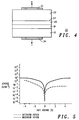
- a device structure 30 fabricated according to the inventive method disclosed herein. More particularly, illustrated is device 30 including substrate 10, seed layer 18, buffer layer 20, and high dielectric constant oxide layer 22. Further included, are a positive metal contact 32 and a negative metal contact 34. Leakage current density is measured across structure of device 30 and resultant values are illustrated graphically in FIG. 5. As illustrated, leakage current density across device structure 30 is decreased due to the utilization of activated oxygen to form the semiconductor structure.
- Illustrated comparatively in FIG. 5 are layers formed with molecular oxygen and layers formed with activated oxygen according to the present invention.
- this method can be used to grow additional oxide layers of the ABO 3 structure, e.g. SrTiO 3 , BaTiO 3 , CaTiO 3 , (Ba, Sr)TiO 3 , or the like.
- this method can be used in a variety of growth deposition methods, including, but not limited to molecular beam epitaxy (MBE), chemical beam epitaxy (CBE), metal-organic molecular beam epitaxy (MOMBE), ultra-high vacuum chemical vapor deposition (UHVCVD), physical vapor deposition (PVD), metal-organic chemical vapor deposition (MOCVD), or the like.
- MBE molecular beam epitaxy
- CBE chemical beam epitaxy
- MOMBE metal-organic molecular beam epitaxy
- UHVCVD ultra-high vacuum chemical vapor deposition
- PVD physical vapor deposition
- MOCVD metal-organic chemical vapor deposition
- the interface of buffer layer, 20 is formed utilizing molecular oxygen.
- the high dielectric constant oxide layer 22 is formed utilizing activated oxygen, thereby providing for reduced leakage current density.
- Activated or atomic oxygen is utilized during the growth step of the oxide layer 22, generated using an RF plasma source, an electron cyclotron resonance (ECR), ozone gas, or the like.
- ECR electron cyclotron resonance
- This method of fabrication provides for reduced leakage current density across the oxide layer 22, thus as a result, processing steps and thermal budgets for CMOS applications are considerably reduced. It should be understood that this method as disclosed can be applied for the growth of a variety of oxide layers in a number of deposition processes.
Landscapes
- Formation Of Insulating Films (AREA)
- Semiconductor Memories (AREA)
- Insulated Gate Type Field-Effect Transistor (AREA)
Abstract
A method for fabricating a semiconductor structure including the steps of
providing a silicon substrate (10) having a surface (12); forming an interface including a
seed layer (18) adjacent to the surface (12) of the silicon substrate (10), forming a buffer
layer (20) utilizing molecular oxygen; and forming one or more layers of a high dielectric
constant oxide (22) on the buffer layer (20) utilizing activated oxygen.
Description
- The present invention relates in general to a method for fabricating a semiconductor structure including a buffer layer between a silicon substrate and metal oxides, and more particularly to a method for fabricating a semiconductor structure including a buffer layer and a high dielectric constant oxide formed using activated oxygen to reduce leakage current density.
- Epitaxial growth of single crystal oxide thin films on silicon is of great interest in numerous device applications, e.g., ferroelectrics or high dielectric constant oxides for non-volatile high density memory and next generation MOS devices. Also, in the preparation of these films, it is pivotal to establish an ordered transition layer or buffer layer on the Si surface, especially for subsequent growth of single crystal oxides, e.g., perovskites.
- Some reported growth of these oxides, such as BaO and BaTiO3 on Si (100) were based on a BaSi2 (cubic) template by depositing one fourth monolayer of Ba on Si (100) using molecular beam epitaxy at temperatures greater than 850°C. See for example: R. McKee et al., Appl. Phys. Lett. 59(7), pp. 782-784 (12 August 1991); R. McKee et al., Appl. Phys. Lett. 63(20), pp. 2818-2820 (15 November 1993); R. McKee et al., Mat. Res. Soc. Symp. Proc., Vol. 21, pp. 131-135 (1991); U.S. Patent No. 5,225,031, issued July 6, 1993, entitled "PROCESS FOR DEPOSITING AN OXIDE EPITAXIALLY ONTO A SILICON SUBSTRATE AND STRUCTURES PREPARED WITH THE PROCESS"; and U.S. Patent No. 5,482,003, issued January 9, 1996, entitled "PROCESS FOR DEPOSITING EPITAXIAL ALKALINE EARTH OXIDE ONTO A SUBSTRATE AND STRUCTURES PREPARED WITH THE PROCESS". A strontium suicide (SrSi2) interface model with a c(4x2) structure was proposed. See for example: R. McKee et al., Phys. Rev. Lett. 81(14), 3014 (5 October 1998). However, atomic level simulation of this proposed structure indicates that it likely is not stable at elevated temperatures.
- Growth of SrTiO3 on silicon (100) using an SrO buffer layer has been accomplished. See for example: T. Tambo et al., Jpn. J. Appl. Phys., Vol. 37 (1998), pp. 4454-4459. However, the SrO buffer layer was thick (100 Å), thereby limiting application for transistor films, and crystallinity was not maintained throughout the growth.
- Furthermore, SrTiO3 has been grown on silicon using thick oxide layers (60-120 Å) of SrO or TiO. See for example: B. K. Moon et al., Jpn. J. Appl. Phys., Vol. 33 (1994), pp. 1472-1477. These thick buffer layers would limit the application for transistors.
- In CMOS applications, these types of oxide layers are fabricated using molecular oxygen and are formed thin (less than 50Å). Accordingly, a result is leaky films in which high electrical leakage is experienced due to oxygen deficiencies or vacancies. Furthermore, these films require a post growth anneal in oxygen to reduce leakage current density across the oxide layer.
- Therefore, a method for fabricating a high dielectric constant oxide on a semiconductor structure having low leakage current density is desired.
- It is a purpose of the present invention to provide for a method of fabricating a high dielectric constant oxide on a semiconductor structure having low leakage current density.
- It is a further purpose of the present invention to provide for a method of fabricating a high dielectric constant oxide on a semiconductor structure in which the gate dielectric leakage current density is near zero.
- It is another purpose of the present invention to provide for a method of fabricating a high dielectric constant oxide on a semiconductor structure using activated or atomic oxygen, thus reducing leakage current density.
- The above problems and others are at least partially solved and the above purposes and others are realized in a method of fabricating a semiconductor structure including the steps of providing a silicon substrate having a surface, forming on the surface of the silicon substrate a buffer layer characterised by a crystalline material formed using molecular oxygen and forming one or more layers of a high dielectric constant oxide on the buffer layer using activated oxygen.
- Referring to the drawings:
- FIG. 1 illustrates a cross-sectional view of a clean semiconductor substrate having a native oxide layer and an oxide layer formed thereon in accordance with the present invention;
- FIG. 2 illustrates a cross-sectional view of the semiconductor structure having a seed layer formed thereon in accordance with the present invention;
- FIG. 3 is a cross-sectional view of the semiconductor substrate of FIG. 2 further showing a buffer layer formed thereon in accordance with the present invention;
- FIG. 4 is a cross-sectional view of the semiconductor substrate of FIG. 3 further showing a high dielectric constant oxide layer and metal contacts for measuring leakage current density across the structure in accordance with the present invention; and
- FIG. 5 illustrates graphically the reduction of leakage current density across the structure of FIG. 4 in accordance with the present invention.
-
- This disclosure teaches a method of fabricating a high dielectric constant (high-k) metal oxide having an interface with a silicon substrate. The process is based on the fabrication of a high dielectric constant oxide layer utilizing activated oxygen. In addition, the process includes the fabrication of a buffer layer as an interface for subsequent growth of the high dielectric constant oxide layer using molecular oxygen. Accordingly, disclosed is a new method of growing perovskite oxides such as SrTiO3, BaTiO3, SrBaTiO3, CaTiO3, or the like utilizing activated oxygen.
- To form the novel interface between a silicon (Si) substrate and one or more layers of a high dielectric constant (high-k) metal oxide(s), various approaches may be used. Included are examples for starting with a Si substrate having silicon dioxide (SiO2) on the surface. The silicon dioxide is disclosed as formed of a native oxide, or utilizing thermal, or chemical techniques. SiO2 is amorphous rather than single crystalline which is desirable for purposes of growing additional single crystal material on the substrate.
- Turning now to the drawings in which like elements are designated with like numbers throughout the FIGs., FIG. 1 illustrates a
Si substrate 10 having asurface 12, and an optional layer 14 of SiO2 thereupon. In this particular embodiment, layer 14 of SiO2 naturally exists (native oxide) once thesilicon substrate 10 is exposed to air (oxygen). Alternatively, layer 14 of SiO2 may be formed purposely in a controlled fashion well known in the art, e.g., thermally by applying oxygen onto thesurface 12 at a high temperature, or chemically using a standard chemical etch process. In an alternative embodiment, layer 14 of SiO2 is removed utilizing thermal desorption of the native oxide, or the like. In this particular embodiment, layer 14 is formed with a thickness in a range of 5-100Å thick, and more particularly with a thickness in a range of 10-25Å. - Next, a thin (e.g few mono-layers) seed layer 18 (as illustrated in FIG. 2) of a silicate nature or the like is formed using either the process of metal reaction with the SiO2 or a metal oxide such as SrO, BaO or the like, to the
surface 15 of SiO2 layer 14 at 0-900°C and under oxygen partial pressure equal to or less than 1 x 10⁻⁴ mBar. This can be accomplished in a molecular beam epitaxy chamber or in a chemical vapor deposition (CVD) or a physical vapor deposition (PVD) chamber under inert ambient conditions. - To fabricate
seed layer 18,substrate 10 is properly heated andsubstrate 10 having SiO2 layer 14 thereon is exposed to a beam of metal, such as strontium (Sr), barium (Ba), calcium (Ca), zirconium (Zr), hafnium (Hf), or the like to react with the SiO2 layer, or to a metal oxide compound such as SrO, BaO or the like utilizing molecular oxygen to form anamorphous oxide 16 onto the SiO2 oxide 14 as illustrated in FIG. 1. - This step provides for the formation of a stable silicate on
silicon substrate 10. The next step is the formation of a high-k oxide layer using molecular oxygen only, this layer is of low resistivity but will serve as a barrier layer thus limiting the oxygen diffusion to the silicon substrate thus limiting the seed layer thickness to few monolayers. During fabrication the thickness ofmetal oxide layer 16 buffer layer is 5-100Å, with a preferred thickness in the range of 15-50Å. This oxide layer is crystalline. - In this particular embodiment, the insertion of a buffer layer between the seed layer and the final oxide layer is crucial in maintaining thin
interface seed layer 18. During fabrication, this growth is monitored using reflection high energy electron diffraction (RHEED) techniques which are well documented in the art and which can be used in situ, i.e., while performing the exposing step within the growth chamber. It will of course be understood that once a specific manufacturing process is provided and followed, it may not be necessary to perform the RHEED techniques on every substrate. Alternatively, monitoring of the crystalline structure can be accomplished utilizing any surface sensitive technique, such as reflection difference spectroscopy (RDS), spectroscopic ellipsometry (SE), or the like wherein the surface is monitored by in situ techniques. - It should be understood by those skilled in the art that the temperatures and pressures given for these processes are recommended for the particular embodiment described, but the invention is not limited to a particular temperature or pressure range. As taught,
seed layer 18 comprises rows of strontium, silicon, and oxygen atoms in a 2x1 configuration on a (001) surface ofsilicon substrate 10, 1x in the 〈110〉 direction and 2x in the orthogonal 〈110〉 direction. - Next, a
buffer layer 20 is formed on asurface 19 ofseed layer 18.Buffer layer 20 is formed by exposing the structure to a beam of metal, such as strontium (Sr), barium (Ba), calcium (Ca), zirconium (Zr), hafnium (Hf), or the like utilizing molecular oxygen to form an oxide onto theseed layer 18 as illustrated in FIG. 3.Buffer layer 20 serves to smooth the surface ofseed layer 18 for the subsequent growth of a high dielectric constant oxide (discussed presently). Buffer layer also serves to preserve the structure ofseed layer 18.Buffer layer 20 is formed to a thickness in a range of 0-100Å. As taught,buffer layer 20 is crystalline. - Next, the formation of a high dielectric
constant oxide layer 22, as illustrated in FIG. 4, is accomplished by either the simultaneous or alternating supply to asurface 23 of thebuffer layer 20 of an alkaline-earth metal and a transition metal at less than or equal to 800°C, more particularly at a temperature in a range of 350-650°C and under a partial pressure of less than or equal to 1x10⁻⁴ mBar of activated oxygen. - Single crystal high dielectric
constant oxide layer 22, more particularly a perovskite, is formed onsurface 23 ofbuffer layer 20 by either the simultaneous or alternating supply of alkaline-earth metal (Sr, Ba etc), activated oxygen, more particularly atomic oxygen, and a transition metal, such as titanium, at less than or equal to 800°C under an activated oxygen partial pressure of less than or equal to 1x10⁻⁴ mBar. This singlecrystal oxide layer 22 may, for example, comprise a thickness of 50-1000Å and will be substantially lattice matched with theunderlying buffer layer 20. - Referring to FIGs. 4 and 5, high dielectric
constant layer 22 when formed in this manner utilizing activated oxygen exhibits a decrease in current leakage of two orders of magnitude, for example 10―2A/cm2 at -1V, than that of oxide layers grown with molecular oxygen. Illustrated in FIG. 4, is adevice structure 30 fabricated according to the inventive method disclosed herein. More particularly, illustrated isdevice 30 includingsubstrate 10,seed layer 18,buffer layer 20, and high dielectricconstant oxide layer 22. Further included, are apositive metal contact 32 and anegative metal contact 34. Leakage current density is measured across structure ofdevice 30 and resultant values are illustrated graphically in FIG. 5. As illustrated, leakage current density acrossdevice structure 30 is decreased due to the utilization of activated oxygen to form the semiconductor structure. Illustrated comparatively in FIG. 5 are layers formed with molecular oxygen and layers formed with activated oxygen according to the present invention. - As disclosed, this method can be used to grow additional oxide layers of the ABO3 structure, e.g. SrTiO3, BaTiO3, CaTiO3, (Ba, Sr)TiO3, or the like. In addition, this method can be used in a variety of growth deposition methods, including, but not limited to molecular beam epitaxy (MBE), chemical beam epitaxy (CBE), metal-organic molecular beam epitaxy (MOMBE), ultra-high vacuum chemical vapor deposition (UHVCVD), physical vapor deposition (PVD), metal-organic chemical vapor deposition (MOCVD), or the like.
- Accordingly, disclosed is a method for fabricating a high dielectric
constant oxide layer 22 for decreased leakage current density in combination withsilicon substrate 10 as described herein. The interface of buffer layer, 20 is formed utilizing molecular oxygen. The high dielectricconstant oxide layer 22 is formed utilizing activated oxygen, thereby providing for reduced leakage current density. Activated or atomic oxygen is utilized during the growth step of theoxide layer 22, generated using an RF plasma source, an electron cyclotron resonance (ECR), ozone gas, or the like. This method of fabrication provides for reduced leakage current density across theoxide layer 22, thus as a result, processing steps and thermal budgets for CMOS applications are considerably reduced. It should be understood that this method as disclosed can be applied for the growth of a variety of oxide layers in a number of deposition processes.
Claims (9)
- A method of fabricating a semiconductor structure characterised by the steps of:providing a silicon substrate (10) having a surface (12);forming on the surface of the substrate a buffer layer (20) utilizing molecular oxygen; andforming one or more layers of a high dielectric constant oxide (22) on the buffer layer utilizing activated oxygen.
- The method of fabricating a semiconductor structure of claim 1 further including the step of forming on the surface of the silicon substrate, between the silicon substrate and the buffer layer, a seed layer (18) characterised by a silicate crystalline material.
- The method of fabricating a semiconductor structure of claim 2 wherein the forming the seed layer (18) step includes forming a 2x1 reconstruction.
- The method of fabricating a semiconductor structure of claim 2 wherein the step of forming a seed layer includes forming the seed layer (18) in one of a UHV environment, a chemical vapor deposition system or a physical vapor deposition system.
- The method of fabricating a semiconductor structure of claim 2 wherein the step of forming a seed layer (18) comprises forming at least a single monolayer of silicon, oxygen, and a metal.
- The method of fabricating a semiconductor structure of claim 2 wherein the step of forming a seed layer further comprises the steps of:forming a silicon oxide layer (14) having a surface;depositing a metal (16) on the surface of the silicon oxide layer; andheating the silicon oxide layer and the metal (16) to form a silicate crystalline material seed layer.
- The method of fabricating a semiconductor structure of claim 6 wherein the metal is selected from the group of strontium, barium, calcium, zirconium, and hafnium.
- The method of fabricating a semiconductor structure of claim 1 wherein the step of forming a buffer layer utilizing molecular oxygen includes forming the buffer layer (20) of a metal oxide selected from the group of strontium and molecular oxygen, barium and molecular oxygen, calcium and molecular oxygen, zirconium and molecular oxygen and hafnium and molecular oxygen.
- The method of fabricating a semiconductor structure of claim 1 wherein the step of forming one or more layers of a high dielectric constant oxide (22) on the buffer layer (20) utilizing activated oxygen includes forming the high dielectric constant oxide selected from the group of strontium, barium, calcium, zirconium and hafnium.
Applications Claiming Priority (2)
| Application Number | Priority Date | Filing Date | Title |
|---|---|---|---|
| US09/354,173 US6270568B1 (en) | 1999-07-15 | 1999-07-15 | Method for fabricating a semiconductor structure with reduced leakage current density |
| US354173 | 1999-07-15 |
Publications (1)
| Publication Number | Publication Date |
|---|---|
| EP1069606A2 true EP1069606A2 (en) | 2001-01-17 |
Family
ID=23392154
Family Applications (1)
| Application Number | Title | Priority Date | Filing Date |
|---|---|---|---|
| EP00115127A Withdrawn EP1069606A2 (en) | 1999-07-15 | 2000-07-12 | Method for fabricating a semiconductor structure with reduced leakage current destiny |
Country Status (7)
| Country | Link |
|---|---|
| US (1) | US6270568B1 (en) |
| EP (1) | EP1069606A2 (en) |
| JP (1) | JP2001068469A (en) |
| KR (1) | KR20010029918A (en) |
| CN (1) | CN1145196C (en) |
| SG (1) | SG85711A1 (en) |
| TW (1) | TW471066B (en) |
Cited By (27)
| Publication number | Priority date | Publication date | Assignee | Title |
|---|---|---|---|---|
| WO2002099897A1 (en) * | 2001-06-01 | 2002-12-12 | Motorola, Inc., A Corporation Of The State Of Delaware | Optically-communicating integrated circuits |
| US6589856B2 (en) | 2001-08-06 | 2003-07-08 | Motorola, Inc. | Method and apparatus for controlling anti-phase domains in semiconductor structures and devices |
| US6638838B1 (en) | 2000-10-02 | 2003-10-28 | Motorola, Inc. | Semiconductor structure including a partially annealed layer and method of forming the same |
| US6639249B2 (en) | 2001-08-06 | 2003-10-28 | Motorola, Inc. | Structure and method for fabrication for a solid-state lighting device |
| US6646293B2 (en) | 2001-07-18 | 2003-11-11 | Motorola, Inc. | Structure for fabricating high electron mobility transistors utilizing the formation of complaint substrates |
| US6667196B2 (en) | 2001-07-25 | 2003-12-23 | Motorola, Inc. | Method for real-time monitoring and controlling perovskite oxide film growth and semiconductor structure formed using the method |
| US6673667B2 (en) | 2001-08-15 | 2004-01-06 | Motorola, Inc. | Method for manufacturing a substantially integral monolithic apparatus including a plurality of semiconductor materials |
| US6673646B2 (en) | 2001-02-28 | 2004-01-06 | Motorola, Inc. | Growth of compound semiconductor structures on patterned oxide films and process for fabricating same |
| US6693033B2 (en) | 2000-02-10 | 2004-02-17 | Motorola, Inc. | Method of removing an amorphous oxide from a monocrystalline surface |
| US6693298B2 (en) | 2001-07-20 | 2004-02-17 | Motorola, Inc. | Structure and method for fabricating epitaxial semiconductor on insulator (SOI) structures and devices utilizing the formation of a compliant substrate for materials used to form same |
| US6709989B2 (en) | 2001-06-21 | 2004-03-23 | Motorola, Inc. | Method for fabricating a semiconductor structure including a metal oxide interface with silicon |
| WO2004053949A1 (en) * | 2002-12-09 | 2004-06-24 | Infineon Technologies Ag | Ferroelectric capacitor and process for its manufacture |
| US6855992B2 (en) | 2001-07-24 | 2005-02-15 | Motorola Inc. | Structure and method for fabricating configurable transistor devices utilizing the formation of a compliant substrate for materials used to form the same |
| US6885065B2 (en) | 2002-11-20 | 2005-04-26 | Freescale Semiconductor, Inc. | Ferromagnetic semiconductor structure and method for forming the same |
| US6916717B2 (en) | 2002-05-03 | 2005-07-12 | Motorola, Inc. | Method for growing a monocrystalline oxide layer and for fabricating a semiconductor device on a monocrystalline substrate |
| US6965128B2 (en) | 2003-02-03 | 2005-11-15 | Freescale Semiconductor, Inc. | Structure and method for fabricating semiconductor microresonator devices |
| US6992321B2 (en) | 2001-07-13 | 2006-01-31 | Motorola, Inc. | Structure and method for fabricating semiconductor structures and devices utilizing piezoelectric materials |
| US7005717B2 (en) | 2000-05-31 | 2006-02-28 | Freescale Semiconductor, Inc. | Semiconductor device and method |
| US7019332B2 (en) | 2001-07-20 | 2006-03-28 | Freescale Semiconductor, Inc. | Fabrication of a wavelength locker within a semiconductor structure |
| US7020374B2 (en) | 2003-02-03 | 2006-03-28 | Freescale Semiconductor, Inc. | Optical waveguide structure and method for fabricating the same |
| US7045815B2 (en) | 2001-04-02 | 2006-05-16 | Freescale Semiconductor, Inc. | Semiconductor structure exhibiting reduced leakage current and method of fabricating same |
| US7067856B2 (en) | 2000-02-10 | 2006-06-27 | Freescale Semiconductor, Inc. | Semiconductor structure, semiconductor device, communicating device, integrated circuit, and process for fabricating the same |
| US7105866B2 (en) | 2000-07-24 | 2006-09-12 | Freescale Semiconductor, Inc. | Heterojunction tunneling diodes and process for fabricating same |
| US7161227B2 (en) | 2001-08-14 | 2007-01-09 | Motorola, Inc. | Structure and method for fabricating semiconductor structures and devices for detecting an object |
| US7169619B2 (en) | 2002-11-19 | 2007-01-30 | Freescale Semiconductor, Inc. | Method for fabricating semiconductor structures on vicinal substrates using a low temperature, low pressure, alkaline earth metal-rich process |
| US7211852B2 (en) | 2001-01-19 | 2007-05-01 | Freescale Semiconductor, Inc. | Structure and method for fabricating GaN devices utilizing the formation of a compliant substrate |
| US7342276B2 (en) | 2001-10-17 | 2008-03-11 | Freescale Semiconductor, Inc. | Method and apparatus utilizing monocrystalline insulator |
Families Citing this family (28)
| Publication number | Priority date | Publication date | Assignee | Title |
|---|---|---|---|---|
| EP1301941A2 (en) * | 2000-07-20 | 2003-04-16 | North Carolina State University | High dielectric constant metal silicates formed by controlled metal-surface reactions |
| US20060252265A1 (en) * | 2002-03-06 | 2006-11-09 | Guangxiang Jin | Etching high-kappa dielectric materials with good high-kappa foot control and silicon recess control |
| US6806095B2 (en) | 2002-03-06 | 2004-10-19 | Padmapani C. Nallan | Method of plasma etching of high-K dielectric materials with high selectivity to underlying layers |
| US7094704B2 (en) * | 2002-05-09 | 2006-08-22 | Applied Materials, Inc. | Method of plasma etching of high-K dielectric materials |
| US6902681B2 (en) * | 2002-06-26 | 2005-06-07 | Applied Materials Inc | Method for plasma etching of high-K dielectric materials |
| US20040007561A1 (en) * | 2002-07-12 | 2004-01-15 | Applied Materials, Inc. | Method for plasma etching of high-K dielectric materials |
| US6855643B2 (en) * | 2002-07-12 | 2005-02-15 | Padmapani C. Nallan | Method for fabricating a gate structure |
| JP4009550B2 (en) * | 2003-03-27 | 2007-11-14 | エルピーダメモリ株式会社 | Method for forming metal oxide film |
| MXPA05010352A (en) * | 2003-03-27 | 2006-03-08 | Constr Res & Tech Gmbh | Liquid coloring suspension. |
| US20060102197A1 (en) * | 2004-11-16 | 2006-05-18 | Kang-Lie Chiang | Post-etch treatment to remove residues |
| US20070202700A1 (en) * | 2006-02-27 | 2007-08-30 | Applied Materials, Inc. | Etch methods to form anisotropic features for high aspect ratio applications |
| US7368394B2 (en) * | 2006-02-27 | 2008-05-06 | Applied Materials, Inc. | Etch methods to form anisotropic features for high aspect ratio applications |
| US7655571B2 (en) * | 2006-10-26 | 2010-02-02 | Applied Materials, Inc. | Integrated method and apparatus for efficient removal of halogen residues from etched substrates |
| US7846845B2 (en) * | 2006-10-26 | 2010-12-07 | Applied Materials, Inc. | Integrated method for removal of halogen residues from etched substrates in a processing system |
| US7946759B2 (en) * | 2007-02-16 | 2011-05-24 | Applied Materials, Inc. | Substrate temperature measurement by infrared transmission |
| US20080203056A1 (en) * | 2007-02-26 | 2008-08-28 | Judy Wang | Methods for etching high aspect ratio features |
| JP2009021584A (en) * | 2007-06-27 | 2009-01-29 | Applied Materials Inc | High temperature material gate structure high temperature etching method |
| US20100330805A1 (en) * | 2007-11-02 | 2010-12-30 | Kenny Linh Doan | Methods for forming high aspect ratio features on a substrate |
| CN101752237B (en) * | 2008-12-16 | 2012-08-08 | 国际商业机器公司 | Formation of high-K gate stacks in semiconductor devices |
| US8992689B2 (en) | 2011-03-01 | 2015-03-31 | Applied Materials, Inc. | Method for removing halogen-containing residues from substrate |
| KR101895307B1 (en) | 2011-03-01 | 2018-10-04 | 어플라이드 머티어리얼스, 인코포레이티드 | Abatement and strip process chamber in a dual loadrock configuration |
| US8845816B2 (en) | 2011-03-01 | 2014-09-30 | Applied Materials, Inc. | Method extending the service interval of a gas distribution plate |
| WO2012148568A1 (en) | 2011-03-01 | 2012-11-01 | Applied Materials, Inc. | Method and apparatus for substrate transfer and radical confinement |
| US11171008B2 (en) | 2011-03-01 | 2021-11-09 | Applied Materials, Inc. | Abatement and strip process chamber in a dual load lock configuration |
| US9533332B2 (en) | 2011-10-06 | 2017-01-03 | Applied Materials, Inc. | Methods for in-situ chamber clean utilized in an etching processing chamber |
| CN106847737B (en) | 2012-02-29 | 2020-11-13 | 应用材料公司 | Decontamination and stripping process chamber in configuration |
| US8932947B1 (en) | 2013-07-23 | 2015-01-13 | Applied Materials, Inc. | Methods for forming a round bottom silicon trench recess for semiconductor applications |
| US9214377B2 (en) | 2013-10-31 | 2015-12-15 | Applied Materials, Inc. | Methods for silicon recess structures in a substrate by utilizing a doping layer |
Family Cites Families (10)
| Publication number | Priority date | Publication date | Assignee | Title |
|---|---|---|---|---|
| US4888202A (en) * | 1986-07-31 | 1989-12-19 | Nippon Telegraph And Telephone Corporation | Method of manufacturing thin compound oxide film and apparatus for manufacturing thin oxide film |
| US5482003A (en) * | 1991-04-10 | 1996-01-09 | Martin Marietta Energy Systems, Inc. | Process for depositing epitaxial alkaline earth oxide onto a substrate and structures prepared with the process |
| US5225031A (en) * | 1991-04-10 | 1993-07-06 | Martin Marietta Energy Systems, Inc. | Process for depositing an oxide epitaxially onto a silicon substrate and structures prepared with the process |
| JP3162718B2 (en) * | 1991-12-13 | 2001-05-08 | サイメトリックス,コーポレイション | Integrated circuit memory |
| EP0568064B1 (en) * | 1992-05-01 | 1999-07-14 | Texas Instruments Incorporated | Pb/Bi-containing high-dielectric constant oxides using a non-Pb/Bi-containing perovskite as a buffer layer |
| US5326721A (en) * | 1992-05-01 | 1994-07-05 | Texas Instruments Incorporated | Method of fabricating high-dielectric constant oxides on semiconductors using a GE buffer layer |
| US5450812A (en) * | 1993-07-30 | 1995-09-19 | Martin Marietta Energy Systems, Inc. | Process for growing a film epitaxially upon an oxide surface and structures formed with the process |
| US5589284A (en) * | 1994-08-01 | 1996-12-31 | Texas Instruments Incorporated | Electrodes comprising conductive perovskite-seed layers for perovskite dielectrics |
| US6088216A (en) * | 1995-04-28 | 2000-07-11 | International Business Machines Corporation | Lead silicate based capacitor structures |
| AU8473998A (en) * | 1998-07-01 | 2000-01-24 | Lockheed Martin Energy Research Corporation | Geometric shape control of thin film ferroelectrics |
-
1999
- 1999-07-15 US US09/354,173 patent/US6270568B1/en not_active Expired - Lifetime
-
2000
- 2000-07-03 SG SG200003693A patent/SG85711A1/en unknown
- 2000-07-11 KR KR1020000039467A patent/KR20010029918A/en not_active Withdrawn
- 2000-07-12 EP EP00115127A patent/EP1069606A2/en not_active Withdrawn
- 2000-07-14 TW TW089114109A patent/TW471066B/en not_active IP Right Cessation
- 2000-07-14 JP JP2000213905A patent/JP2001068469A/en active Pending
- 2000-07-14 CN CNB001202553A patent/CN1145196C/en not_active Expired - Fee Related
Cited By (28)
| Publication number | Priority date | Publication date | Assignee | Title |
|---|---|---|---|---|
| US7067856B2 (en) | 2000-02-10 | 2006-06-27 | Freescale Semiconductor, Inc. | Semiconductor structure, semiconductor device, communicating device, integrated circuit, and process for fabricating the same |
| US6693033B2 (en) | 2000-02-10 | 2004-02-17 | Motorola, Inc. | Method of removing an amorphous oxide from a monocrystalline surface |
| US7005717B2 (en) | 2000-05-31 | 2006-02-28 | Freescale Semiconductor, Inc. | Semiconductor device and method |
| US7105866B2 (en) | 2000-07-24 | 2006-09-12 | Freescale Semiconductor, Inc. | Heterojunction tunneling diodes and process for fabricating same |
| US6638838B1 (en) | 2000-10-02 | 2003-10-28 | Motorola, Inc. | Semiconductor structure including a partially annealed layer and method of forming the same |
| US7211852B2 (en) | 2001-01-19 | 2007-05-01 | Freescale Semiconductor, Inc. | Structure and method for fabricating GaN devices utilizing the formation of a compliant substrate |
| US6673646B2 (en) | 2001-02-28 | 2004-01-06 | Motorola, Inc. | Growth of compound semiconductor structures on patterned oxide films and process for fabricating same |
| US7045815B2 (en) | 2001-04-02 | 2006-05-16 | Freescale Semiconductor, Inc. | Semiconductor structure exhibiting reduced leakage current and method of fabricating same |
| WO2002099897A1 (en) * | 2001-06-01 | 2002-12-12 | Motorola, Inc., A Corporation Of The State Of Delaware | Optically-communicating integrated circuits |
| US6709989B2 (en) | 2001-06-21 | 2004-03-23 | Motorola, Inc. | Method for fabricating a semiconductor structure including a metal oxide interface with silicon |
| US6992321B2 (en) | 2001-07-13 | 2006-01-31 | Motorola, Inc. | Structure and method for fabricating semiconductor structures and devices utilizing piezoelectric materials |
| US6646293B2 (en) | 2001-07-18 | 2003-11-11 | Motorola, Inc. | Structure for fabricating high electron mobility transistors utilizing the formation of complaint substrates |
| US6693298B2 (en) | 2001-07-20 | 2004-02-17 | Motorola, Inc. | Structure and method for fabricating epitaxial semiconductor on insulator (SOI) structures and devices utilizing the formation of a compliant substrate for materials used to form same |
| US7019332B2 (en) | 2001-07-20 | 2006-03-28 | Freescale Semiconductor, Inc. | Fabrication of a wavelength locker within a semiconductor structure |
| US6855992B2 (en) | 2001-07-24 | 2005-02-15 | Motorola Inc. | Structure and method for fabricating configurable transistor devices utilizing the formation of a compliant substrate for materials used to form the same |
| US6667196B2 (en) | 2001-07-25 | 2003-12-23 | Motorola, Inc. | Method for real-time monitoring and controlling perovskite oxide film growth and semiconductor structure formed using the method |
| US6639249B2 (en) | 2001-08-06 | 2003-10-28 | Motorola, Inc. | Structure and method for fabrication for a solid-state lighting device |
| US6589856B2 (en) | 2001-08-06 | 2003-07-08 | Motorola, Inc. | Method and apparatus for controlling anti-phase domains in semiconductor structures and devices |
| US7161227B2 (en) | 2001-08-14 | 2007-01-09 | Motorola, Inc. | Structure and method for fabricating semiconductor structures and devices for detecting an object |
| US6673667B2 (en) | 2001-08-15 | 2004-01-06 | Motorola, Inc. | Method for manufacturing a substantially integral monolithic apparatus including a plurality of semiconductor materials |
| US7342276B2 (en) | 2001-10-17 | 2008-03-11 | Freescale Semiconductor, Inc. | Method and apparatus utilizing monocrystalline insulator |
| US6916717B2 (en) | 2002-05-03 | 2005-07-12 | Motorola, Inc. | Method for growing a monocrystalline oxide layer and for fabricating a semiconductor device on a monocrystalline substrate |
| US7169619B2 (en) | 2002-11-19 | 2007-01-30 | Freescale Semiconductor, Inc. | Method for fabricating semiconductor structures on vicinal substrates using a low temperature, low pressure, alkaline earth metal-rich process |
| US6885065B2 (en) | 2002-11-20 | 2005-04-26 | Freescale Semiconductor, Inc. | Ferromagnetic semiconductor structure and method for forming the same |
| US7031138B2 (en) | 2002-12-09 | 2006-04-18 | Infineon Technologies Ag | Ferroelectric capacitor and process for its manufacture |
| WO2004053949A1 (en) * | 2002-12-09 | 2004-06-24 | Infineon Technologies Ag | Ferroelectric capacitor and process for its manufacture |
| US6965128B2 (en) | 2003-02-03 | 2005-11-15 | Freescale Semiconductor, Inc. | Structure and method for fabricating semiconductor microresonator devices |
| US7020374B2 (en) | 2003-02-03 | 2006-03-28 | Freescale Semiconductor, Inc. | Optical waveguide structure and method for fabricating the same |
Also Published As
| Publication number | Publication date |
|---|---|
| SG85711A1 (en) | 2002-01-15 |
| CN1145196C (en) | 2004-04-07 |
| US6270568B1 (en) | 2001-08-07 |
| CN1281246A (en) | 2001-01-24 |
| KR20010029918A (en) | 2001-04-16 |
| TW471066B (en) | 2002-01-01 |
| JP2001068469A (en) | 2001-03-16 |
Similar Documents
| Publication | Publication Date | Title |
|---|---|---|
| US6270568B1 (en) | Method for fabricating a semiconductor structure with reduced leakage current density | |
| EP1069605B1 (en) | Method for fabricating a semiconductor structure including a metal oxide interface with silicon | |
| US6241821B1 (en) | Method for fabricating a semiconductor structure having a crystalline alkaline earth metal oxide interface with silicon | |
| US6224669B1 (en) | Method for fabricating a semiconductor structure having a crystalline alkaline earth metal oxide interface with silicon | |
| EP1108805B1 (en) | Method for fabricating a semiconductor structure having a stable crystalline interface with silicon | |
| US6248459B1 (en) | Semiconductor structure having a crystalline alkaline earth metal oxide interface with silicon | |
| US6709989B2 (en) | Method for fabricating a semiconductor structure including a metal oxide interface with silicon | |
| EP1109212B1 (en) | Semiconductor structure having a crystalline alkaline earth metal silicon nitride/oxide interface with silicon | |
| US6501121B1 (en) | Semiconductor structure | |
| EP1096042A1 (en) | Method for fabricating a semiconductor structure including a metal oxide interface with silicon | |
| US7851365B1 (en) | Methods for preparing semiconductor substrates and interfacial oxides thereon | |
| KR20030051820A (en) | Semiconductor structure having high dielectric constant material |
Legal Events
| Date | Code | Title | Description |
|---|---|---|---|
| PUAI | Public reference made under article 153(3) epc to a published international application that has entered the european phase |
Free format text: ORIGINAL CODE: 0009012 |
|
| AK | Designated contracting states |
Kind code of ref document: A2 Designated state(s): AT BE CH CY DE DK ES FI FR GB GR IE IT LI LU MC NL PT SE |
|
| AX | Request for extension of the european patent |
Free format text: AL;LT;LV;MK;RO;SI |
|
| STAA | Information on the status of an ep patent application or granted ep patent |
Free format text: STATUS: THE APPLICATION HAS BEEN WITHDRAWN |
|
| 18W | Application withdrawn |
Effective date: 20031020 |