EP1069552B1 - Verfahren zur Zusammenstellung einer Gruppe, die zumindest ein erstes und ein zweites Element aufweist, wobei eines der Elemente eine Mikrostruktur ohne Verpackung umfasst - Google Patents
Verfahren zur Zusammenstellung einer Gruppe, die zumindest ein erstes und ein zweites Element aufweist, wobei eines der Elemente eine Mikrostruktur ohne Verpackung umfasst Download PDFInfo
- Publication number
- EP1069552B1 EP1069552B1 EP99830449A EP99830449A EP1069552B1 EP 1069552 B1 EP1069552 B1 EP 1069552B1 EP 99830449 A EP99830449 A EP 99830449A EP 99830449 A EP99830449 A EP 99830449A EP 1069552 B1 EP1069552 B1 EP 1069552B1
- Authority
- EP
- European Patent Office
- Prior art keywords
- regions
- wafer
- process according
- forming
- region
- Prior art date
- Legal status (The legal status is an assumption and is not a legal conclusion. Google has not performed a legal analysis and makes no representation as to the accuracy of the status listed.)
- Expired - Lifetime
Links
Images


Classifications
-
- G—PHYSICS
- G11—INFORMATION STORAGE
- G11B—INFORMATION STORAGE BASED ON RELATIVE MOVEMENT BETWEEN RECORD CARRIER AND TRANSDUCER
- G11B5/00—Recording by magnetisation or demagnetisation of a record carrier; Reproducing by magnetic means; Record carriers therefor
- G11B5/48—Disposition or mounting of heads or head supports relative to record carriers ; arrangements of heads, e.g. for scanning the record carrier to increase the relative speed
- G11B5/56—Disposition or mounting of heads or head supports relative to record carriers ; arrangements of heads, e.g. for scanning the record carrier to increase the relative speed with provision for moving the head support for the purpose of adjusting the position of the head relative to the record carrier, e.g. manual adjustment for azimuth correction or track centering
-
- B—PERFORMING OPERATIONS; TRANSPORTING
- B81—MICROSTRUCTURAL TECHNOLOGY
- B81C—PROCESSES OR APPARATUS SPECIALLY ADAPTED FOR THE MANUFACTURE OR TREATMENT OF MICROSTRUCTURAL DEVICES OR SYSTEMS
- B81C1/00—Manufacture or treatment of devices or systems in or on a substrate
- B81C1/00865—Multistep processes for the separation of wafers into individual elements
- B81C1/00896—Temporary protection during separation into individual elements
-
- H—ELECTRICITY
- H10—SEMICONDUCTOR DEVICES; ELECTRIC SOLID-STATE DEVICES NOT OTHERWISE PROVIDED FOR
- H10W—GENERIC PACKAGES, INTERCONNECTIONS, CONNECTORS OR OTHER CONSTRUCTIONAL DETAILS OF DEVICES COVERED BY CLASS H10
- H10W72/00—Interconnections or connectors in packages
- H10W72/50—Bond wires
- H10W72/531—Shapes of wire connectors
- H10W72/5363—Shapes of wire connectors the connected ends being wedge-shaped
-
- H—ELECTRICITY
- H10—SEMICONDUCTOR DEVICES; ELECTRIC SOLID-STATE DEVICES NOT OTHERWISE PROVIDED FOR
- H10W—GENERIC PACKAGES, INTERCONNECTIONS, CONNECTORS OR OTHER CONSTRUCTIONAL DETAILS OF DEVICES COVERED BY CLASS H10
- H10W74/00—Encapsulations, e.g. protective coatings
- H10W74/10—Encapsulations, e.g. protective coatings characterised by their shape or disposition
- H10W74/15—Encapsulations, e.g. protective coatings characterised by their shape or disposition on active surfaces of flip-chip devices, e.g. underfills
Definitions
- the present invention relates to a process for assembling a group comprising at least one first and one second element, one of the elements comprising a microstructure without package.
- hard disks are the most commonly used data storage solution; consequently they are produced in very large volumes, and the maximum density of data storage is increasing year by year.
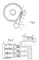
- Hard disks are read and written by actuator devices, the general structure whereof is shown in Figures 1 and 2, and is described hereinafter.
- Figure 1 shows an actuator device 1 of known rotary type, which comprises a motor 2 (also known as a voice coil motor) secured to a support body 3 which is generally known as E block, owing to its "E" shape in lateral view (see Figure 2).
- the support body 3 has a plurality of arms 4 which each support a suspension 5 formed by a cantilevered plate.
- each suspension 5 supports a R/W transducer 6 for reading/writing, which in an operative condition is disposed facing a surface of a hard disk 7, so as to perform roll and pitch movements in order to follow the surface of the hard disk 7.
- R/W transducer 6 (which is also called picoslider or slider) is bonded to a coupling called gimbal or flexure 8, which is generally formed from the suspension 5 and comprises for example a rectangular plate 8a, cut on three and a half sides from the plate of the suspension 5, and having a portion 8b connected to the suspension 5 and allowing bending of plate 8a caused by the weight of the R/W transducer 6 (see Figure 3).
- gimbal or flexure 8 which is generally formed from the suspension 5 and comprises for example a rectangular plate 8a, cut on three and a half sides from the plate of the suspension 5, and having a portion 8b connected to the suspension 5 and allowing bending of plate 8a caused by the weight of the R/W transducer 6 (see Figure 3).
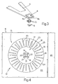
- the second actuation stage comprises a microactuator interposed between the R/W transducer 6, as shown in Figure 3, which shows exploded the end of the suspension 5, the gimbal 8, the R/W transducer 6 and a microactuator 10, in this case of the rotary type.
- the microactuator 10 is controlled by a signal supplied by control electronics, on the basis of a tracking error.
- the microactuator 10 comprises fixed parts and suspended mobile parts.
- the latter during assembly of the R/W transducer on the microactuator and when forming connections with the control circuitry, may be displaced and/or may collapse.
- stresses may be set up in the structure of the microactuator, such as to cause fragility of the structure.
- the aim of the invention is thus to provide an assembly process that enables protection of microstructures when assembled on other components in a simple and inexpensive way.
- a process for assembling a group comprising at least one first and one second element and a unit thus assembled are provided, as defined in Claims 1 and 18, respectively.
- microactuator 10 on the slider 6 and on the suspension 5, as shown in Figure 3.
- the microactuators and the corresponding control circuits are first formed (for example, as described in the European Patent Application EP-A-0 913 921).
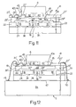
- FIG 4 a first semiconductor material wafer 11 is shown, wherein a plurality of microactuators 10 is formed, only one of which is shown as regards its essential elements.
- the microactuator 10 comprises an external stator 13, designed to be rigidly connected to the plate 8a of the gimbal 8 ( Figure 3), and an internal rotor 14 capacitively coupled to the stator 13 and designed to be bonded to the R/W transducer 6 ( Figure 3).
- the rotor 14 comprises a suspended mass 15 of a substantially annular shape and a plurality of mobile arms 16 extending radially outwards starting from the suspended mass 15.
- the suspended mass 15 surrounds concentrically an anchoring region 21, which is fixed and is separated from the suspended mask 15 by an annular trench 18 connected to four radial slots 19, which extend radially inside the suspended mass 15.
- Four elastic suspension and anchoring elements, hereinafter called springs 20, extend between the anchoring region 21 and the suspended mass 15 inside the radial slots 19.
- the springs 20 have the function of elastically and electrically connecting the suspended mass 15 to the anchoring region 21.
- the stator 13 comprises a fixed region 22, surrounding the area housing the rotor 14, and a plurality of fixed arms 23, which extend radially from the fixed region 22 and are arranged so that they alternate with the mobile arms 16.
- the mobile arms 16 and the fixed arms 23 are separated from one another by a trench 24 which extends in zigzag fashion annularly between the fixed region 22 and the suspended mass 15.
- the fixed region 22 houses biasing regions for the rotor 14 and the stator 13, components of the control circuitry, as well as the connections between the microactuator and the control circuitry, in a per se known manner, and hence not shown.
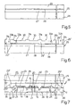
- a second wafer 25 is made which houses a plurality of supporting and protective structures, one for each microactuator 10 present in the first wafer 11.
- the second wafer 25 is bonded to the wafer 11 so as to support and protect the microactuators 10 during cutting of the wafer 11 and bonding to the slider 6 and to the gimbal 8.
- the second wafer 25 comprises a monocrystalline silicon substrate 26, a silicon oxide blocking layer 27 deposited or thermally grown, an insulation layer 28, for example made of silicon nitride, and a polycrystalline silicon layer 29.
- the substrate 26 has an initial thickness of 650-700 ⁇ m.
- the polycrystalline silicon layer 29 is made preferably by depositing a polycrystalline silicon germ layer and performing an epitaxial growth until a total thickness of approximately 5 ⁇ m is obtained.
- the polycrystalline silicon layer 29 is masked with resist mask and etched out to form cavities 30, having a thickness of between approximately 5 and 10 ⁇ m, separated by projections 31a and 31b ( Figure 6).
- the projections 31a preferably with an annular shape, are each formed at a respective suspended mass 15 of the first wafer 11, while the projections 31b are each formed at a respective fixed region 22, as shown in Figure 7 for a microactuator 10.
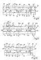
- first trenches 33a and second trenches 33b which extend up to the blocking layer 27.
- the first trenches 33a which are narrower, have a preferably annular shape and are arranged so that each of them extends approximately along or near the circumference that externally delimits the region of the first wafer 11 which houses the respective rotor 14, this circumference separating the rotor 14 from the respective fixed region 22.
- the second trenches 33b which are wider, are arranged along the scribing lines of the wafers 11 and 25. In a way not shown, trenches are also made at the contact pads of the first wafer 11.
- the polycrystalline silicon layer 29 forms mobile intermediate regions 29' and fixed intermediate regions 29", separated from each other by the first trenches 33a.
- the fixed intermediate regions 29" corresponding to adjacent microactuators 10 are separated from one another by the second trenches 33b.
- the second wafer 25 is thinned out from the back in a mechanical way, for example by grinding the substrate 26, preferably until a total thickness of 300-400 ⁇ m is obtained.
- the second wafer 25 is then bonded to the first wafer 11 so that the projections 31a face the suspended masses 15, and the projections 31b face the fixed regions 22, as shown in Figure 7, in which the reference number 35 designates a substrate region of the first wafer 11, from which the anchoring region 21 extends; number 36 designates insulating regions, for example of silicon oxide regions, which electrically separate the fixed region 22 from the substrate region 35, where necessary; number 37 designates the bonding material, and number 38 an air gap extending beneath the suspended mass 15 and the mobile arms 16.
- a composite wafer 39 is obtained, which is subsequently mechanically thinned out, for example by grinding, so reducing the thickness of the substrate 26 of the second wafer 25 to approximately 30 ⁇ m. Then, the substrate 26 of the second wafer 25 is completely removed by wet etching or plasma etching, which is stopped at the blocking layer 27, as shown in Figure 8.
- the blocking layer 27 is then masked and etched so as to be removed completely from the areas where metallic regions of electrical connection are to be made and at the contact pads of the first wafer 11 (in a way not shown).
- blocking regions 27' remain at the trenches 33a and 33b and where the electrical connections for the slider are to be made.
- the blocking regions 27' form, together with the mobile intermediate regions 29' and fixed intermediate regions 29", a unitary protection and blocking structure, which completely covers all the microactuators 10 formed in the first wafer 11 and blocks the mobile parts, so preventing them from being displaced or from collapsing.
- a metallic multilayer is laid and defined (for example, formed by an aluminum layer and a gold layer) so as to obtain metallic regions 40a and connection lines 40b that extend partly on the insulating layer 28 and partly on the regions 27'.
- the metallic regions 40a extend approximately over the suspended masses 15, and the connection lines 40b each extend between a peripheral portion of the mobile intermediate region 29' and the portion, which faces the latter, of the respective fixed intermediate region 29", passing over the first trenches 33a, as shown in Figure 9.
- a test is then carried out on the composite wafer 39 in order to verify whether any short circuits are present.
- the composite wafer 39 is cut into single units 41 at the trenches 33b, as shown in Figure 10.
- the individual microactuators 10 are covered by the protective and blocking structure formed by the regions 29', 29" and 27', so that the operation of cutting will not damage the microactuators 10.
- Figure 11 a slider 6 is bonded on each unit 41.
- bonding material 42 is interposed between the metallic region 40a and the underside of the slider 6.
- connection lines 40b are bonded to contact pads 43 present on the slider 6 by means of conductive material 44, using, for example, a laser soft bonding technique, and the metallic region 40b is bonded to the body of the slider 6 by means of a conductive glue 45 so as to provide a ground connection for the slider 6.
- each unit 41 is bonded on a respective suspension 5 at the plate 8a using a bonding material 47.
- the connection lines 40b are electrically connected to respective contact pads 48 provided on the plate 8a by means of conductive wires 49, and the contact pads present on the first wafer 11 (not shown) are electrically connected to respective contact pads 50 provided on the plate 8a by means of electrical wires 51, which are visible only in part.
- the blocking regions 27' are etched away using hydrofluoric acid gas to obtain the final structure shown in cross-sectional view in Figure 13 and in perspective view in Figure 14.
- the mobile parts of the microactuator 10 (suspended mass 15 and mobile arms 16) and the slider 6, which is fixed to the aforesaid mobile parts through the mobile intermediate region 29', are free to move with respect to the fixed parts (fixed arms 23, fixed region 22 and fixed intermediate region 29").
- the electrical connections 40 are free and have the necessary elasticity to enable rotation of the slider 6 with respect to the fixed intermediate region 29".
- the process enables the unit made up of the microactuator 10 and the slider 6 to be assembled on the suspension 5 and enables the latter to be assembled on the supporting body 3 in a traditional way, as in standard actuator devices not having the microactuator 10.
- it provides a structure for protecting the microactuator 10 when cutting the wafer 11 and subsequently during assembly and bonding, so reducing the risks of damage and collapse.
- the described process comprises typical steps of microelectronics fabrication techniques, and hence has a high reliability and reproducibility, along with contained costs.
- microactuator may moreover be made of polycrystalline silicon or a metallic material, according to any known technique of fabrication.
- the first step of reducing the thickness of the substrate 26 of the second wafer 25 may be omitted; however, this step is advantageous in order to reduce to the minimum the grinding time after bonding of the wafers 11 and 25, and consequently in order to reduce the risks of damage to the microactuators 10.
Landscapes
- Engineering & Computer Science (AREA)
- Manufacturing & Machinery (AREA)
- Microelectronics & Electronic Packaging (AREA)
- Micromachines (AREA)
- Supporting Of Heads In Record-Carrier Devices (AREA)
- Moving Of Heads (AREA)
- Magnetic Heads (AREA)
- Moving Of The Head To Find And Align With The Track (AREA)
- Adjustment Of The Magnetic Head Position Track Following On Tapes (AREA)
Claims (23)
- Verfahren zum Zusammenstellen einer Gruppe bzw. Anordnung, welche aufweist: wenigstens ein erstes Element (10) und ein zweites Element (6), wobei das erste Element (10) eine Mikrostruktur ohne Gehäuse aufweist, wobei das Verfahren die Schritte aufweist:- Bilden eines ersten Wafers (11) als Halbleitermaterial, welcher eine Vielzahl von Mikrostrukturen (10) aufweist, welche erste (15, 16) und zweite (22, 23) Betriebsbereiche beinhaltet, welche voneinander durch erste Gräben (24) getrennt sind,durch folgende Schritte gekennzeichnet:- Bilden eines zweiten Wafers (25) aus Halbleitermaterial, welches Sperrbereiche (27, 27') aufweist, welche eine Vielzahl von ersten (29') und zweiten (29") Zwischenbereichen verbindet, wobei der erste und der zweite Zwischenbereich durch zweite Gräben (33a) voneinander getrennt sind;- Verbinden des ersten Wafers (11) und des zweiten Wafers (25), um so einen Verbundwafer (39) zu bilden, in welchem die ersten Betriebsbereiche (15, 16) an den ersten Zwischenbereichen (29') befestigt sind und wobei die zweiten Betriebsbereiche (22, 23) an den zweiten Zwischenbereichen (29") befestigt sind;- Schneiden des Verbundwafers (39) in eine Vielzahl von Einheiten (41), wobei jede Einheit (41) wenigstens einen ersten Betriebsbereich und einen zweiten Betriebsbereich, und einen ersten Zwischenbereich und einen zweiten Zwischenbereich beinhaltet;- Befestigen des ersten Zwischenbereichs (29') von wenigstens einer Einheit (41) an dem zweiten Element (6); und- Entfernen der Sperrbereiche (27').
- Verfahren nach Anspruch 1, dadurch gekennzeichnet, dass der Schritt des Bildens eines zweiten Wafers den Schritt des Bildens wenigstens einer Sperrschicht (27) aufweist, und dadurch, dass nach dem Schritt des Verbindens der Schritt des teilweisen Entfernens der Sperrschicht (27) durchgeführt wird, um so die Sperrschichten (27') wenigstens bei den zweiten Gräben (33a) zu bilden.
- Verfahren nach Anspruch 2, dadurch gekennzeichnet, dass der Schritt des Bildens eines zweiten Wafers (25) die Schritte aufweist von:- Bilden eines Substrates (26) aus Halbleitermaterial;- Bilden der Sperrschicht (27) auf der oberen Seite des Substrats;- Bilden einer Halbleiterschicht (29) auf der oberen Seite der Sperrschicht; und- Bilden von zweiten Gräben (33a) in der Halbleiterschicht, so dass dadurch erste und zweite Zwischenbereiche (29', 29") erhalten werden.
- Verfahren nach Anspruch 3, dadurch gekennzeichnet, dass es ferner den Schritt des Bildens von Hohlräumen (30) in der Halbleiterschicht (29) aufweist, wobei die Hohlräume herausragende Teile (31a, 31b) in den ersten und zweiten Zwischenbereichen (29', 29") begrenzen, und dadurch, dass der Schritt des Verbindens den Schritt des Bondens bzw. Anschließens der herausragenden Teile (31a, 31b) an den ersten und zweiten Betriebsbereichen (15, 22) aufweist.
- Verfahren nach Anspruch 3 oder 4, dadurch gekennzeichnet, dass das Substrat (26) aus polykristallinem Silicium hergestellt wird; wobei der Schritt des Bildens einer Sperrschicht (27) den Schritt des Bildens einer Siliciumoxidschicht aufweist und der Schritt des Bildens einer Halbleiterschicht (29) den Schritt des epitaxialen Wachsens einer polykristallinen Siliciumschicht aufweist.
- Verfahren nach einem der Ansprüche 3-5, dadurch gekennzeichnet, dass vor dem Schritt des Verbindens des ersten Wafers (11) und des zweiten Wafers (25) ein Schritt des vorläufigen Reduzierens der Dicke des Substrates (26) durchgeführt wird.
- Verfahren nach einem der Ansprüche 3-6, dadurch gekennzeichnet, dass vor dem Schritt des Schneidens der Schritt des vollständigen Entfernens des Substrates (26) durchgeführt wird.
- Verfahren nach Anspruch 7, dadurch gekennzeichnet, dass der Schritt des vollständigen Entfernens des Substrates (26) einen Schritt des mechanischen Reduzierens der Dicke des Substrates und nachfolgendes komplettes Ätzen des Substrates aufweist.
- Verfahren nach Anspruch 8, dadurch gekennzeichnet, dass der Schritt des mechanischen Reduzierens durch Schleifen ausgeführt wird und der Schritt des vollständigen Ätzens durch Nassätzen oder Plasmaätzen ausgeführt wird.
- Verfahren nach einem der vorausgehenden Ansprüche, dadurch gekennzeichnet, dass vor dem Schritt des Schneidens der Schritt des Bildens leitender Bereiche (40a, 40b) ausgeführt wird, welche sich über die Sperrbereiche (27') und die ersten und zweiten Zwischenbereiche (29', 29") erstrecken.
- Verfahren nach Anspruch 10, dadurch gekennzeichnet, dass die leitenden Bereiche elektrische Anschlussleitungen (40b) und metallische Bereiche (40a) aufweisen, wobei sich die elektrischen Anschlussleitungen (40b) über die Sperrbereiche (27') und die zweiten Gräben (33a) erstrecken und sich die metallischen Bereiche (40a) über die ersten Zwischenbereiche (29') erstrecken; wobei der Schritt des Befestigens den Schritt des Bondens bzw. Anschließens des zweiten Elementes (6) an einen metallischen Bereich (40a) aufweist, welcher sich über den ersten Zwischenbereich (29') der wenigstens einen Einheit (41) erstreckt.
- Verfahren nach Anspruch 10 oder 11, dadurch gekennzeichnet, dass nach dem Schritt des Bildens leitender Bereiche (40a, 40b) der Schritt des Bildens elektrischer Anschlussstrukturen (44, 45) zwischen dem zweiten Element (6) und den leitenden Bereichen (40a, 40b) ausgeführt wird.
- Verfahren nach einem der vorausgehenden Ansprüche, dadurch gekennzeichnet, dass vor dem Schritt des Entfernens der Sperrbereiche (27') der Schritt des Befestigens der Einheit (41) an einem Stützelement (8a) ausgeführt wird.
- Verfahren nach Anspruch 13, dadurch gekennzeichnet, dass der Schritt des Befestigens der Einheit (41) an einem Stützelement (8a) den Schritt des Bondens eines Substratbereiches (35) des ersten Wafers (11) an das Stützelement (8a) aufweist.
- Verfahren nach Anspruch 14, dadurch gekennzeichnet, dass nach dem Schritt des Bondens der Schritt des elektrischen Verbindens des zweiten Elementes (6) und des ersten Wafers (11) an das Stützelement (8a) durchgeführt wird.
- Verfahren nach einem der vorausgehenden Ansprüche, dadurch gekennzeichnet, dass die Sperrbereiche (27') aus Siliciumoxid hergestellt werden und dass der Schritt des Entfernens der Sperrbereiche (27') das Ätzen des Siliciumoxids in Fluorwasserstoffsäure-Gas aufweist.
- Verfahren nach einem der vorausgehenden Ansprüche, dadurch gekennzeichnet, dass die Einheit (41) zu einer Festplatten-Leseeinheit gehört, und dadurch, dass die Mikrostruktur einen Mikroaktuator aufweist und das zweite Element (6) einen Lese-/Schreibwandler aufweist.
- Einheit, welche wenigstens ein erstes Element (10) und ein zweites Element (6) aufweist, wobei das erste Element eine Mikrostruktur (10) aufweist, welche einen ersten Betriebsbereich (15) und einen zweiten Betriebsbereich (22) aufweist, welche voneinander durch einen ersten Graben (24) getrennt sind,
gekennzeichnet durch eine Befestigungsstruktur (29', 29"), welche zwischen dem ersten Element (10) und dem zweiten Element (6) liegt, wobei die Befestigungsstruktur einen ersten Zwischenbereich (29') und einen zweiten Zwischenbereich (29") beinhaltet, welche voneinander durch einen zweiten Graben (33a) getrennt sind;
wobei der erste Betriebsbereich (15) an dem ersten Zwischenbereich (29') befestigt ist und der zweite Betriebsbereich (22) an dem zweiten Zwischenbereich (29") befestigt ist; und wobei der erste Zwischenbereich (29') an dem zweiten Element (6) befestigt ist. - Einheit nach Anspruch 18, dadurch gekennzeichnet, dass der erste Zwischenbereich (29') und der zweite Zwischenbereich (29") herausragende Teile (31a, 31b) besitzen, welche an dem ersten Betriebsbereich (15) und dem zweiten Betriebsbereich (22) mit Hilfe eines Bondmaterials (37) befestigt sind.
- Einheit nach Anspruch 18 oder 19, dadurch gekennzeichnet, dass die Befestigungsstruktur (29', 29") ein polykristallines Silicium aufweist.
- Einheit nach einem der Ansprüche 18-20, gekennzeichnet durch freie elektrische Anschlüsse (40b), welche sich auf einer Seite der Befestigungsstruktur (29', 29") erstrecken, wobei die Seite, welche dem zweiten Element (6) gegenüberliegt, zwischen dem ersten Zwischenbereich (29') und dem zweiten Zwischenbereich (29"), über den zweiten Graben (33a) hinweg gehen.
- Einheit nach einem der Ansprüche 18-21, ferner durch ein Stützelement (8a) gekennzeichnet, welches an der Mikrostruktur (10) befestigt ist.
- Festplatten-Leseeinheit nach einem der Ansprüche 18-22, in welcher die Mikrostruktur (10) einen Mikroaktuator aufweist und das zweite Element (6) einen Lese-/Schreibwandler aufweist.
Priority Applications (4)
| Application Number | Priority Date | Filing Date | Title |
|---|---|---|---|
| DE69933370T DE69933370D1 (de) | 1999-07-15 | 1999-07-15 | Verfahren zur Zusammenstellung einer Gruppe, die zumindest ein erstes und ein zweites Element aufweist, wobei eines der Elemente eine Mikrostruktur ohne Verpackung umfasst |
| EP99830449A EP1069552B1 (de) | 1999-07-15 | 1999-07-15 | Verfahren zur Zusammenstellung einer Gruppe, die zumindest ein erstes und ein zweites Element aufweist, wobei eines der Elemente eine Mikrostruktur ohne Verpackung umfasst |
| US09/616,227 US6391741B1 (en) | 1999-07-15 | 2000-07-14 | Fabrication process for microstructure protection systems related to hard disk reading unit |
| JP2000214947A JP3420184B2 (ja) | 1999-07-15 | 2000-07-14 | 少なくとも1つの第1要素および1つの第2要素を備えるグループを組み立てる方法、および、そのように組み立てられたユニット |
Applications Claiming Priority (1)
| Application Number | Priority Date | Filing Date | Title |
|---|---|---|---|
| EP99830449A EP1069552B1 (de) | 1999-07-15 | 1999-07-15 | Verfahren zur Zusammenstellung einer Gruppe, die zumindest ein erstes und ein zweites Element aufweist, wobei eines der Elemente eine Mikrostruktur ohne Verpackung umfasst |
Publications (2)
| Publication Number | Publication Date |
|---|---|
| EP1069552A1 EP1069552A1 (de) | 2001-01-17 |
| EP1069552B1 true EP1069552B1 (de) | 2006-09-27 |
Family
ID=8243503
Family Applications (1)
| Application Number | Title | Priority Date | Filing Date |
|---|---|---|---|
| EP99830449A Expired - Lifetime EP1069552B1 (de) | 1999-07-15 | 1999-07-15 | Verfahren zur Zusammenstellung einer Gruppe, die zumindest ein erstes und ein zweites Element aufweist, wobei eines der Elemente eine Mikrostruktur ohne Verpackung umfasst |
Country Status (4)
| Country | Link |
|---|---|
| US (1) | US6391741B1 (de) |
| EP (1) | EP1069552B1 (de) |
| JP (1) | JP3420184B2 (de) |
| DE (1) | DE69933370D1 (de) |
Families Citing this family (1)
| Publication number | Priority date | Publication date | Assignee | Title |
|---|---|---|---|---|
| EP1617178B1 (de) * | 2004-07-12 | 2017-04-12 | STMicroelectronics Srl | Mikroelektromechanische Struktur mit elektrisch isolierten Gebieten und Verfahren zu ihrer Herstellung |
Family Cites Families (6)
| Publication number | Priority date | Publication date | Assignee | Title |
|---|---|---|---|---|
| US4784970A (en) * | 1987-11-18 | 1988-11-15 | Grumman Aerospace Corporation | Process for making a double wafer moated signal processor |
| DE59304431D1 (de) * | 1993-05-05 | 1996-12-12 | Litef Gmbh | Mikromechanische Beschleunigungsmessvorrichtung und Verfahren zu deren Herstellung |
| DE19602318C1 (de) * | 1996-01-23 | 1997-08-14 | Fraunhofer Ges Forschung | Verfahren zum Verbinden von mikromechanischen Wafern |
| US5882532A (en) * | 1996-05-31 | 1999-03-16 | Hewlett-Packard Company | Fabrication of single-crystal silicon structures using sacrificial-layer wafer bonding |
| US5914801A (en) * | 1996-09-27 | 1999-06-22 | Mcnc | Microelectromechanical devices including rotating plates and related methods |
| EP0913921B1 (de) * | 1997-10-29 | 2006-05-03 | STMicroelectronics S.r.l. | Verfahren zur Herstellung einer Halbleiter Microantrieb, insbesondere für Lese-Schreibekopf einem Festplattengerät, und so hergestellter Microantrieb |
-
1999
- 1999-07-15 DE DE69933370T patent/DE69933370D1/de not_active Expired - Lifetime
- 1999-07-15 EP EP99830449A patent/EP1069552B1/de not_active Expired - Lifetime
-
2000
- 2000-07-14 US US09/616,227 patent/US6391741B1/en not_active Expired - Lifetime
- 2000-07-14 JP JP2000214947A patent/JP3420184B2/ja not_active Expired - Fee Related
Also Published As
| Publication number | Publication date |
|---|---|
| EP1069552A1 (de) | 2001-01-17 |
| DE69933370D1 (de) | 2006-11-09 |
| US6391741B1 (en) | 2002-05-21 |
| JP2001077300A (ja) | 2001-03-23 |
| JP3420184B2 (ja) | 2003-06-23 |
Similar Documents
| Publication | Publication Date | Title |
|---|---|---|
| US7463454B2 (en) | Micro-actuator for hard drive utilizing insulating portions to separate biasing regions from adjacent regions of the micro-actuator and simplified manufacture process therefore | |
| US6781286B2 (en) | Piezoelectric driving device | |
| US5742452A (en) | Low mass magnetic recording head and suspension | |
| US8193550B2 (en) | Method for manufacturing a micro-electro-mechanical device, in particular an optical microswitch, and micro-electro-mechanical device thus obtained | |
| JP5261453B2 (ja) | 圧電素子の製造方法 | |
| US6689627B2 (en) | Process for manufacturing micromechanical components in a semiconductor material wafer with reduction in the starting wafer thickness | |
| US20010009776A1 (en) | Method for manufacturing a semiconductor material integrated microactuator, in particular for a hard disc mobile read/write head, and a microactuator obtained thereby | |
| EP0711416A1 (de) | Siliziumbeschleunigungsmesser mit elektrostatischer kraftkompensation | |
| US6697232B1 (en) | Bonded transducer-level electrostatic microactuator for disc drive system | |
| US20030161071A1 (en) | Slider for a data storage device including transducer level micro-positioning and method of fabrication therefor | |
| US6446326B1 (en) | Method for manufacturing a hard disk read/write unit, with micrometric actuation | |
| EP1069552B1 (de) | Verfahren zur Zusammenstellung einer Gruppe, die zumindest ein erstes und ein zweites Element aufweist, wobei eines der Elemente eine Mikrostruktur ohne Verpackung umfasst | |
| EP1031965B1 (de) | Mikrometrische Betätigung, Festplatten Lese-/Schreibeinheit | |
| US6638836B1 (en) | Process for manufacturing a group comprising at least two elements, one whereof includes an encapsulated micro-integrated structure, and thereby obtained group | |
| US6483671B2 (en) | Microintegrated structure with protection against contaminating particles | |
| US6396174B1 (en) | Method for manufacturing a microintegrated structure with buried connections, in particular an integrated microactuator for a hard-disk drive unit | |
| JP4040621B2 (ja) | ディスク・ドライブ・システム用の、トランスデューサ・レベルのマイクロアクチュエータ及びそれを製造するための改善された方法 | |
| JP3515503B2 (ja) | マイクロメカニズムの互いに対して移動可能な2つの部分を電気的に接続する浮遊部材の製造方法 | |
| US20020097530A1 (en) | Method of fabricating electrically isolated metal MEMS beams and microactuator incorporating the MEMS beam |
Legal Events
| Date | Code | Title | Description |
|---|---|---|---|
| PUAI | Public reference made under article 153(3) epc to a published international application that has entered the european phase |
Free format text: ORIGINAL CODE: 0009012 |
|
| AK | Designated contracting states |
Kind code of ref document: A1 Designated state(s): DE FR GB IT |
|
| AX | Request for extension of the european patent |
Free format text: AL;LT;LV;MK;RO;SI |
|
| 17P | Request for examination filed |
Effective date: 20010628 |
|
| AKX | Designation fees paid |
Free format text: DE FR GB IT |
|
| GRAP | Despatch of communication of intention to grant a patent |
Free format text: ORIGINAL CODE: EPIDOSNIGR1 |
|
| GRAS | Grant fee paid |
Free format text: ORIGINAL CODE: EPIDOSNIGR3 |
|
| GRAA | (expected) grant |
Free format text: ORIGINAL CODE: 0009210 |
|
| RTI1 | Title (correction) |
Free format text: PROCESS FOR ASSEMBLING A GROUP COMPRISING AT LEAST ONE FIRST AND ONE SECOND ELEMENT, ONE OF THE ELEMENTS COMPRISING A MICROSTRUCTURE WITHOUT PACKAGE |
|
| AK | Designated contracting states |
Kind code of ref document: B1 Designated state(s): DE FR GB IT |
|
| PG25 | Lapsed in a contracting state [announced via postgrant information from national office to epo] |
Ref country code: IT Free format text: LAPSE BECAUSE OF FAILURE TO SUBMIT A TRANSLATION OF THE DESCRIPTION OR TO PAY THE FEE WITHIN THE PRE;WARNING: LAPSES OF ITALIAN PATENTS WITH EFFECTIVE DATE BEFORE 2007 MAY HAVE OCCURRED AT ANY TIME BEFORE 2007. THE CORRECT EFFECTIVE DATE MAY BE DIFFERENT FROM THE ONE RECORDED.SCRIBED TIME-LIMIT Effective date: 20060927 |
|
| REG | Reference to a national code |
Ref country code: GB Ref legal event code: FG4D |
|
| REF | Corresponds to: |
Ref document number: 69933370 Country of ref document: DE Date of ref document: 20061109 Kind code of ref document: P |
|
| PG25 | Lapsed in a contracting state [announced via postgrant information from national office to epo] |
Ref country code: DE Free format text: LAPSE BECAUSE OF FAILURE TO SUBMIT A TRANSLATION OF THE DESCRIPTION OR TO PAY THE FEE WITHIN THE PRESCRIBED TIME-LIMIT Effective date: 20061228 |
|
| ET | Fr: translation filed | ||
| PLBE | No opposition filed within time limit |
Free format text: ORIGINAL CODE: 0009261 |
|
| STAA | Information on the status of an ep patent application or granted ep patent |
Free format text: STATUS: NO OPPOSITION FILED WITHIN TIME LIMIT |
|
| 26N | No opposition filed |
Effective date: 20070628 |
|
| PGFP | Annual fee paid to national office [announced via postgrant information from national office to epo] |
Ref country code: IT Payment date: 20070725 Year of fee payment: 9 |
|
| PG25 | Lapsed in a contracting state [announced via postgrant information from national office to epo] |
Ref country code: IT Free format text: LAPSE BECAUSE OF NON-PAYMENT OF DUE FEES Effective date: 20080715 |
|
| PGFP | Annual fee paid to national office [announced via postgrant information from national office to epo] |
Ref country code: GB Payment date: 20100628 Year of fee payment: 12 |
|
| GBPC | Gb: european patent ceased through non-payment of renewal fee |
Effective date: 20110715 |
|
| PG25 | Lapsed in a contracting state [announced via postgrant information from national office to epo] |
Ref country code: GB Free format text: LAPSE BECAUSE OF NON-PAYMENT OF DUE FEES Effective date: 20110715 |
|
| PGFP | Annual fee paid to national office [announced via postgrant information from national office to epo] |
Ref country code: FR Payment date: 20120806 Year of fee payment: 14 |
|
| REG | Reference to a national code |
Ref country code: FR Ref legal event code: ST Effective date: 20140331 |
|
| PG25 | Lapsed in a contracting state [announced via postgrant information from national office to epo] |
Ref country code: FR Free format text: LAPSE BECAUSE OF NON-PAYMENT OF DUE FEES Effective date: 20130731 |