EP1069460A1 - Reflective lcd device and method of manufacture thereof - Google Patents
Reflective lcd device and method of manufacture thereof Download PDFInfo
- Publication number
- EP1069460A1 EP1069460A1 EP00902021A EP00902021A EP1069460A1 EP 1069460 A1 EP1069460 A1 EP 1069460A1 EP 00902021 A EP00902021 A EP 00902021A EP 00902021 A EP00902021 A EP 00902021A EP 1069460 A1 EP1069460 A1 EP 1069460A1
- Authority
- EP
- European Patent Office
- Prior art keywords
- metal reflection
- liquid crystal
- substrate
- layer
- film
- Prior art date
- Legal status (The legal status is an assumption and is not a legal conclusion. Google has not performed a legal analysis and makes no representation as to the accuracy of the status listed.)
- Granted
Links
Images
Classifications
-
- G—PHYSICS
- G02—OPTICS
- G02F—OPTICAL DEVICES OR ARRANGEMENTS FOR THE CONTROL OF LIGHT BY MODIFICATION OF THE OPTICAL PROPERTIES OF THE MEDIA OF THE ELEMENTS INVOLVED THEREIN; NON-LINEAR OPTICS; FREQUENCY-CHANGING OF LIGHT; OPTICAL LOGIC ELEMENTS; OPTICAL ANALOGUE/DIGITAL CONVERTERS
- G02F1/00—Devices or arrangements for the control of the intensity, colour, phase, polarisation or direction of light arriving from an independent light source, e.g. switching, gating or modulating; Non-linear optics
- G02F1/01—Devices or arrangements for the control of the intensity, colour, phase, polarisation or direction of light arriving from an independent light source, e.g. switching, gating or modulating; Non-linear optics for the control of the intensity, phase, polarisation or colour
- G02F1/13—Devices or arrangements for the control of the intensity, colour, phase, polarisation or direction of light arriving from an independent light source, e.g. switching, gating or modulating; Non-linear optics for the control of the intensity, phase, polarisation or colour based on liquid crystals, e.g. single liquid crystal display cells
- G02F1/133—Constructional arrangements; Operation of liquid crystal cells; Circuit arrangements
- G02F1/1333—Constructional arrangements; Manufacturing methods
- G02F1/1335—Structural association of cells with optical devices, e.g. polarisers or reflectors
- G02F1/133509—Filters, e.g. light shielding masks
- G02F1/133512—Light shielding layers, e.g. black matrix
-
- G—PHYSICS
- G02—OPTICS
- G02F—OPTICAL DEVICES OR ARRANGEMENTS FOR THE CONTROL OF LIGHT BY MODIFICATION OF THE OPTICAL PROPERTIES OF THE MEDIA OF THE ELEMENTS INVOLVED THEREIN; NON-LINEAR OPTICS; FREQUENCY-CHANGING OF LIGHT; OPTICAL LOGIC ELEMENTS; OPTICAL ANALOGUE/DIGITAL CONVERTERS
- G02F1/00—Devices or arrangements for the control of the intensity, colour, phase, polarisation or direction of light arriving from an independent light source, e.g. switching, gating or modulating; Non-linear optics
- G02F1/01—Devices or arrangements for the control of the intensity, colour, phase, polarisation or direction of light arriving from an independent light source, e.g. switching, gating or modulating; Non-linear optics for the control of the intensity, phase, polarisation or colour
- G02F1/13—Devices or arrangements for the control of the intensity, colour, phase, polarisation or direction of light arriving from an independent light source, e.g. switching, gating or modulating; Non-linear optics for the control of the intensity, phase, polarisation or colour based on liquid crystals, e.g. single liquid crystal display cells
- G02F1/133—Constructional arrangements; Operation of liquid crystal cells; Circuit arrangements
- G02F1/1333—Constructional arrangements; Manufacturing methods
- G02F1/1335—Structural association of cells with optical devices, e.g. polarisers or reflectors
- G02F1/133553—Reflecting elements
-
- G—PHYSICS
- G02—OPTICS
- G02F—OPTICAL DEVICES OR ARRANGEMENTS FOR THE CONTROL OF LIGHT BY MODIFICATION OF THE OPTICAL PROPERTIES OF THE MEDIA OF THE ELEMENTS INVOLVED THEREIN; NON-LINEAR OPTICS; FREQUENCY-CHANGING OF LIGHT; OPTICAL LOGIC ELEMENTS; OPTICAL ANALOGUE/DIGITAL CONVERTERS
- G02F1/00—Devices or arrangements for the control of the intensity, colour, phase, polarisation or direction of light arriving from an independent light source, e.g. switching, gating or modulating; Non-linear optics
- G02F1/01—Devices or arrangements for the control of the intensity, colour, phase, polarisation or direction of light arriving from an independent light source, e.g. switching, gating or modulating; Non-linear optics for the control of the intensity, phase, polarisation or colour
- G02F1/13—Devices or arrangements for the control of the intensity, colour, phase, polarisation or direction of light arriving from an independent light source, e.g. switching, gating or modulating; Non-linear optics for the control of the intensity, phase, polarisation or colour based on liquid crystals, e.g. single liquid crystal display cells
- G02F1/133—Constructional arrangements; Operation of liquid crystal cells; Circuit arrangements
- G02F1/1333—Constructional arrangements; Manufacturing methods
- G02F1/1335—Structural association of cells with optical devices, e.g. polarisers or reflectors
- G02F1/133509—Filters, e.g. light shielding masks
- G02F1/133514—Colour filters
Definitions
- This invention relates to a reflection-type liquid crystal display device which uses natural light as a light source and selectively reflects incident natural light by a reflection Film to perform a display and a fabricating method thereof.
- a reflection-type liquid crystal display device is a liquid crystal display device using natural light as a light source and does not need a light source such as a backlight, and is composed of a liquid crystal layer, a pair of transparent insulating substrates holding the liquid crystal layer therebetween, a polarizing film, a metal reflection plate (or film), and the like.
- a conventional twisted nematic (TN) or super twisted nematic (STN) liquid crystal display device needs two polarizing films, whereby 3/4 of natural light is lost, resulting in a dark display.
- the metal reflection plate must be positioned outside the polarizing films, in other words, it must be disposed outside the insulating substrate, and thus there occurs a problem that when light is made incident from a slanting direction on the reflection-type liquid crystal display device, reflected light which is recognized as an image delivers double images on a surface on the liquid crystal layer side of one insulating substrate and on a surface of the metal reflection plate. Moreover, since a pixel through which the incident light passes and a pixel through which the reflected light passes are different, there are problems that contrast is lowered and that when a color display is performed using a color filter, a mixture of colors occurs, resulting in deterioration in color reproduction.
- a TN or STN liquid crystal display device capable of display with one polarizing film and a guest-host liquid crystal display device of a phase-transition type capable of display without using any polarizing films are proposed.
- the polarizing films can be reduced in number or may not be used, thereby making a display brighter.
- the metal reflection plate can be provided on the liquid crystal layer side of one insulating substrate, and thus it is possible to solve the aforesaid problems of double images, decrease in contrast, color mixture of the color filters and the like.
- a conventional black matrix must be formed by patterning metal chromium, chromium oxide, or a black resin between adjacent pixels with high accuracy.
- a material for a metal reflection plate or film is a metal film of aluminum, silver, or an alloy of them with which a high reflectance can be obtained.
- the metal reflection film made of a metal film is corroded and removed since the alkali solution is used in the step of developing the color filter layer in the fabrication process of forming the color filter layer on the metal reflection film.
- This invention is made to solve the aforesaid problems in the conventional reflection-type liquid crystal display device. Objects thereof are to provide a bright display by using only one polarizing film, to enable an excellent black display and a display with excellent contrast by giving a function which is equal to that of the black matrix without necessity of patterning of the light absorbing layer, and to prevent the metal reflection film from being corroded and removed when the color filter is formed on the metal reflection film.
- this invention provides a reflection-type liquid crystal display device with the following structure and a fabricating method thereof.
- the reflection-type liquid crystal display device is a reflection-type liquid crystal display device, in which a first substrate composed of an insulating transparent substrate and a second substrate composed of an insulating substrate are opposed to each other with a liquid crystal layer therebetween, a transparent first electrode is provided on the liquid crystal layer side of the first substrate and a transparent second electrode is provided on the liquid crystal layer side of the second substrate respectively, a color filter layer is provided on the liquid crystal layer side of the first substrate or the second substrate, a metal reflection film is provided between the second substrate and the color filter, a polarizing film is disposed on the opposite side of the first substrate to the liquid crystal layer, and a region where the first electrode and the second electrode overlap in a plane view becomes a pixel, is characterized by the following points.
- the metal reflection film is disposed with a gap between adjacent pixels, that a conductive light absorbing layer electrically connecting with the metal reflection film is provided between the second substrate and the metal reflection film, and that a transparent anodic oxide film is provided on a surface of the metal reflection film.
- the metal reflection film is provided only within a region to be a pixel. It is possible that the metal reflection film is made of aluminum or an aluminum alloy and the conductive light absorbing layer is made of chromium film.
- a fabricating method of a reflection-type liquid crystal display according to this invention comprises the following steps.
- the steps are:
- a chromium film is provided as the light absorbing layer. It is suitable that in the step of providing the metal reflection film layer, an aluminum layer or an aluminum alloy layer is provided as the metal reflection film layer.
- the metal reflection films are provided in each pixel portion, the light absorbing layer is provided on the opposite side of the metal reflection films to the liquid crystal layer, that is, on the entire face on the rear of the metal reflection films, and the light absorbing layer exists also within the gaps between the metal reflection films of the adjacent pixels.
- the light absorbing layer functions in the same manner as a black matrix at the gaps between the pixels, thereby obtaining an excellent black display and also a display with high contrast.
- a transparent anodic oxide film is provided between the metal reflection film and the color filter layer.
- the metal reflection film is protected by the anodic oxide film in the step of developing the color filter layer using an alkali solution, thereby preventing corrosion of the metal reflection film by the alkali solution, so that removal of the metal reflection film never occurs.
- the anodic oxide film is formed by performing anodic oxidation processing for the surface of the metal reflection film with the conductive light absorbing layer which is electrically connected to each metal reflection film as a common electrode.
- an anodic oxidation voltage can be supplied to all the metal reflection films with the conductive light absorbing layer which is provided between the second substrate and the metal reflection films as a common electrode and the metal oxide films can be formed on the entire surfaces of the metal reflection films including side faces, whereby corrosion from the side faces of the metal reflection films can also be prevented.
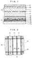
- FIG. 1 and FIG. 2 Reflection-type liquid crystal display device
- FIG. 1 is a schematic sectional view showing part of the reflection-type liquid crystal display device
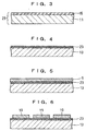
- FIG. 2 is a plane view showing plane positional relations between a light absorbing layer, first electrodes, second electrodes, and metal reflection films in FIG. 1.
- a first substrate 11 composed of a glass substrate that is an insulating transparent substrate and a second substrate 13 composed of an insulating substrate are opposed to each other with a liquid crystal layer 21 therebetween, and transparent first electrodes 15 are provided on the liquid crystal layer 21 side of the first substrate 11 and transparent second electrodes 18 are provided on the liquid crystal layer 21 side of the second substrate 13 respectively.
- the second substrate 13 may not be a transparent substrate.
- the liquid crystal layer 21 is composed of a super twisted nematic liquid crystal aligned at a twist angle of 240° and sealed between an upper substrate 29 and a lower substrate 31 of which peripheries are bonded together with a sealing material not shown.
- the upper substrate 29 is composed of the first substrate 11 and the first electrodes
- the lower substrate 31 is composed of the second substrate 13 and the second electrodes 18 and additionally a light absorbing layer 23, metal reflection films 19, transparent anodic oxide films 25, color filter layers 33, and an over coat layer 35 which will be described later.
- the conductive light absorbing layer 23 made of chromium film is provided on the entire face of at least a display region of a face on the liquid crystal layer 21 side of the second substrate 13, and the metal reflection films 19 made of an aluminum film are provided on a face on the liquid crystal layer 21 side of the light absorbing layer 23.
- Pattern forms of the metal reflection films 19 form a large number of isolated rectangular patterns with a long side length of 290 ⁇ m, a short side length of 90 ⁇ m, and a spaced gap of 10 ⁇ m as shown by broken lines in FIG. 2.
- Three metal reflection films 19 are provided to a region of each pixel portion (a square region of 290 ⁇ m ⁇ 290 ⁇ m), gaps of 10 ⁇ m are provided between metal reflection films 19 and between adjacent pixels, and the light absorbing layer exists in each gap (shown by cross-hatching in FIG. 2). Further, all of the metal reflection films 19 are electrically connected by the conductive light absorbing layer.
- the transparent anodic oxide film (metal oxide film) 25 that is an aluminum oxide film formed by anodic oxidation processing of aluminum film is provided.
- the color filter layer 33 is provided on each of the metal reflection films 19. This color filter layer 33 is formed so that a color filter of a different color is arranged to each of the metal reflection films 19 in one pixel region.
- the color filter layers 33 in which a red color filter R, a green color filter G, and a blue color filter B are arranged from the left in order without gap in relation to three metal reflection films 19 provided in one pixel region are provided.
- the color filter layers 33 are formed so that the top faces thereof become a flat face, the transparent over coat film 35 is provided on the top faces (faces on the liquid crystal layer 21 side), and the transparent second electrodes 18 are provided on the face on the liquid crystal layer 21 side of the transparent over coat film 35.
- the second electrodes 18 are formed in a plurality of stripe-form patterns each having a width of 290 ⁇ m at spaced gaps of 10 ⁇ m at positions aligned with the short side of each metal reflection film 19 on the light absorbing layer 23 as shown in FIG. 2.
- Regions where the first electrodes 15 of the upper substrate 29 and the second electrodes 18 of the lower substrate 31 intersect correspond to regions where each metal reflection film 19 is provided, and a pixel portion is formed by the intersecting portion.
- a polarizing film 27 is provided on the opposite side (the visible side) of the first substrate 11 to the liquid crystal layer 21. Furthermore, a retardation plate 26 is provided between the first substrate 11 and the polarizing film 27 in this example to prevent coloring due to birefringence effects of the liquid crystal layer 21, but this retardation plate 26 is not necessary.
- a voltage applied between the first electrodes 15 and the second electrodes 18 is changed (ON/OFF) at the pixel portions where the first electrodes 15 and the second electrodes 18 intersect to thereby drive the liquid crystal layer 21 so as to phase-modulate light passing therethrough.
- the light absorbing layer 23 is allowed to function as a black matrix, whereby an excellent black display and a color display with good contrast and without mixture of colors can be performed. More than that, it is sufficient to use only one polarizing film 27, thereby enabling a bright display.
- the anodic oxide films 25 are formed on the surfaces of the metal reflection films 19, the surfaces of the metal reflection films 19 are never corroded by an alkali developing solution nor removed in a developing process of the color filter layers 33, resulting in a highly reliable reflection-type liquid crystal display device.
- each metal reflection film 19 is formed only in the pixel portion so that gaps are provided at all of the surroundings of each pixel portion, that is, all portions between adjacent pixels in this embodiment, but the reflection-type liquid crystal display device of this invention is not limited to this, each metal reflection film 19 may be disposed so that a gap is provided at least at one portion between adjacent pixels.
- the metal reflection films 19 are shaped into the same form as the stripe-form patterns of the first electrodes 15 and are placed so that a gap is provided between two pixels adjacent to each other in a width direction. The more gaps there are between adjacent pixels, the more regions there are in a black state regardless of phase modulation of the liquid crystal layer 21, thereby obtaining a better black display.
- color filter layers 33 are provided at the lower substrate 31 side in the aforesaid embodiment, they may be provided at the upper substrate 29 side, that is, on a face on the liquid crystal layer 21 side of the first substrate 11.
- the over coat film 35 made of transparent resin is provided on the entire face on the liquid crystal layer 21 side of the color filter layers 33, and the first electrodes 15 in stripe forms are provided on the surface of the over coat film 35.
- the lower substrate 31 it is suitable to provide a transparent resin film in place of the color filter layers 33 on the light absorbing film 23 and the metal reflection films 19 on which the anodic oxide films 25 are formed, on the liquid crystal layer 21 side of the second substrate 13 and to provide the second electrodes 18 in stripe forms on the surface of the transparent resin film.
- a transparent conductive film made of indium tin oxide film is film-formed on one face of the first substrate 11 that is a transparent glass substrate shown in FIG. 3 to have a film thickness of 110 nm by the sputtering method.
- a positive-type photoresist is applied on the entire face of the transparent conductive film by spin coating, and photography processing by exposure processing and developing processing using a photomask is performed, whereby the photoresist is formed into the pattern forms of the first electrodes 15.
- the etching processing of the transparent conductive film made of indium tin oxide film is performed by wet etching processing using a mixed solution of ferric chloride and hydrochloric acid. Then, the photoresist used as the etching mask is removed by a wet removal method using a resist removing solution, for example, N-320 (trade name) manufactured by Nagase &Co., Ltd.
- the pattern forms of the first electrodes 15 are a large number of stripe-form patterns with a width of 90 ⁇ m and a spaced gap of 10 ⁇ m as shown in FIG. 2.
- An alignment film (not shown) is formed to cover the tops of the first electrodes 15 to thereby form the upper substrate 29.
- the conductive light absorbing layer 23 made of chromium film is formed to have a film thickness of 200 nm by the sputtering method at least on the entire face of the display region of one face of the second substrate 13 composed of an insulating substrate as shown in FIG. 4.
- an aluminum film 9 is formed to have a film thickness of 200 nm as a metal reflection film layer on the light absorbing layer 23 by the sputtering method as shown in FIG. 5.
- a positive-type photoresist is applied on the entire top face of the aluminum film 9 by spin coating, and photolithography processing by exposure processing and development processing using a photomask is performed to pattern the photoresist into the pattern forms of the metal reflection films 19.
- patterning is performed by the etching processing of the aluminum film through use of the photoresist as an etching mask to form many metal reflection films 19 as shown in FIG. 6.
- the etching process of the aluminum film is performed by wet etching using a mixed solution of phosphoric acid, nitric acid, and acetic acid.
- the light absorbing layer 23 made of chromium film composing the light absorbing layer 23 is exposed within a region in which the metal reflection film layer made of aluminum film is etched, and the chromium film of the light absorbing layer 23 is not etched by the aforesaid mixed solution.
- the light absorbing layer 23 is exposed in the gaps between the metal reflection films 19 which are formed in a plurality of isolated rectangular patterns.
- the pattern forms of the metal reflection films 19 are formed into a plurality of isolated rectangular patterns with a long side length of 290 ⁇ m, a short side length of 90 ⁇ m, and a spaced gap of 10 ⁇ m as shown in FIG. 7. These three metal reflection films 19 correspond to each region of three primary colors composing one pixel for a color display.
- the photoresist which has been used as an etching mask is removed by the wet removal method using a resist removing solution, for example, N-320 (trade name) manufactured by Nagase & Co., Ltd.
- anodic oxidation processing using an ammonium phosphate solution as an anodic oxidizing solution is performed for the surfaces of the metal reflection films 19 made of aluminum film with the conductive light absorbing layer 23 made of chromium film as a common electrode.
- the metal reflection films 19 here are formed in a plurality of isolated rectangular patterns, and each metal reflection film 19 is individually electrically connected to the conductive light absorbing layer 23 made of chromium film, so that the transparent anodic oxide film 25 made of aluminum oxide film can be formed on the surface on the metal reflection film 19 made of an aluminum film to cover the entire surface including side faces of the metal reflection film 19 with the light absorbing layer 23 as a common electrode.
- an anodic oxidation voltage which is applied between the conductive light absorbing layer 23 and opposed electrodes 3 is set at a voltage of 40V by a direct current variable power source 5 and the voltage is raised at a speed of 1.5V/min. from 0V, and anodic oxidation processing is performed for one hour at the set voltage after the voltage reaches the set voltage, thereby forming the anodic oxide film 25 with a film thickness of 50 nm.
- a pigment-dispersed type of red color resist V-259R (trade name) with photosensitivity manufactured by Nippon Steel Chemical Co., Ltd. is applied by the spin coating on the metal reflection films 19 of which the entire surfaces are covered with the transparent anodic oxide films 25 to have a film thickness of 1.2 ⁇ m and subjected to exposure processing using a photomask.
- the portion which has been subjected to developing processing by the alkali developing solution and exposed becomes insoluble to the developing solution, and the red color filter R of the color filter layers 33 shown in FIG. 9 is formed by patterning so as to cover every one of three metal reflection films 19 in each pixel region.
- firing is performed for two hours within a temperature range of 220°C to 240°C, thereby thermally curing the red color resist composing the red color filter R and gasifying unreacted substances which are not involved in light curing nor heat curing contained in the red color resist, to remove them.
- a green color filter G and a blue color filter B are similarly formed by patterning in order using a green color resist and a blue color resist respectively so as to cover different one of three metal reflection films 19 in each pixel region.
- the color filter layers 33 composed of the red color filter R, the green color filter G, and the blue color filter B are formed as shown in FIG. 9.
- each of the color filters R, G, and B of the color filter layers 33 are a plurality of isolated rectangular patterns each of which is larger in size than the metal reflection film 19, more specifically, a long side length of 300 ⁇ m and a short side length of 100 ⁇ m. Further, each rectangular pattern is formed such that the center thereof corresponds to the center of each metal reflection film 19 and the long side and the short side thereof are respectively parallel to the long side and the short side of the rectangular pattern of the metal reflection film 19 which is formed in each pixel portion.
- Optoma SS 6777 (trade name) manufactured by JSR is formed on the color filter layers 33 as the transparent over coat film 35 as shown in FIG. 10 by spin coating.
- the over coat film 35 is formed to have a film thickness of 3 ⁇ m.
- the over coat film 35 performs the function of improving the color filter layers 33 in chemical resistance, sputtering resistance, and flatness.
- a transparent conductive film made of indium tin oxide film is formed on the over coat film 35 by the sputtering method to have a film thickness of 110 nm.
- a positive-type photoresist is applied on the entire face of the transparent conductive film by spin coating, and photolithography processing by exposure processing and development processing using a photomask is performed to form the photoresist into the pattern forms of the second electrodes 18.
- the etching processing of the transparent conductive film is performed by the wet etching processing using a mixed solution of ferric chloride and hydrochloric acid. Thereafter, the photoresist used as the etching mask is removed by the wet removal method using a resist removing solution.
- the pattern forms of the second electrodes 18 are a plurality of stripe patterns with a width of 290 ⁇ m and a spaced gap of 10 ⁇ m, and are formed so that the long side thereof and the short side of the rectangular pattern of the metal reflection film 19 overlap each other in parallel.
- an alignment film (not shown) is formed so as to cover the tops of the second electrodes 18, thereby forming the lower substrate 31.
- the upper substrate 29 and the lower substrate 31 which are made as described above are arranged so that the first electrodes 15 on the first substrate 11 and the second electrodes 18 on the second substrate 13 are opposed to each other as shown in FIG. 1, and the stripe-form pattern of the first electrodes 15 and the stripe-form pattern of the second electrodes 18 are orthogonal to each other and the long side of the stripe-form pattern of the first electrodes 15 and the long side of the rectangular pattern of each of the metal reflection films 19 overlap each other in parallel as shown in FIG. 2.
- a pixel portion is formed at a portion where the first electrodes 15 and the second electrodes 18 intersect.
- the metal reflection film 19 which is formed into an isolated rectangular pattern is formed only in each pixel portion. Furthermore, the liquid crystal layer 21 is sealed between the upper substrate 29 and the lower substrate 31 by sealant (not shown).
- the liquid crystal layer 21 is composed of a super twisted nematic liquid crystal which is aligned at a twist angle of 240° .
- the retardation film 26 and the polarizing film 27 are disposed on the opposite side (the visible side) of the first substrate 11 to the liquid crystal layer 21, thereby completing the reflection-type liquid crystal display device shown in FIG. 1.
- the color filter layers 33 are formed directly on the metal reflection films 19 in the conventional fabricating method of the reflection-type liquid crystal display device. Therefore, there is a problem that in the developing process of the color filter layers 33, the aluminum films composing the metal reflection films 19 are exposed within the regions where the color filter layers 33 are developed and corroded by the alkali developing solution.
- the anodic oxide films 25 made of aluminum oxide film are formed to cover the entire faces of the metal reflection films 19 before the color filter layers 33 are formed on the metal reflection films 19.
- This aluminum oxide film is excellent in chemical resistance to the alkali developing solution.
- the metal reflection films 19 are never removed in the developing process of the color filter layers 33.
- a reflection-type liquid crystal display device is provided with a conductive light absorbing layer on the entire face between the second substrate and the metal reflection films which are arranged to provide gaps between adjacent pixels.
- incident light reaches the gap between the adjacent pixels is all absorbed by the light absorbing layer, so that the gap between the adjacent pixels can be brought to a state of usually black regardless of phase modulation by the liquid crystal layer.
- the light absorbing layer is allowed to function in the same manner as a black matrix even if not patterned with high accuracy between pixels, thereby enabling an excellent black display and a color display with high brightness and high contrast and without mixture of colors, so that a reflection-type liquid crystal display device with high quality can be obtained.
- the metal reflection film is never corroded nor removed by the alkali developing solution in a developing process of the color filter layer, resulting in improved reliability.
- the anodic oxide film is formed by anodic oxidation processing of the metal reflection film with the conductive light absorbing layer which is electrically connected to each metal reflection film as a common electrode.
- the anodic oxide films can be formed on the entire faces of all the metal reflection films including side faces, and the metal reflection films are never corroded nor removed from the side faces by the alkali developing solution in the developing process of the color filter layers, with the result that a more reliable reflection-type liquid crystal display device can be obtained.
- the reflection-type liquid crystal display device can be widely used for a portable device such as a portable phone, an electronic desk calculator, a timepiece, or the like, or display devices of other various kinds of electronic equipment.
Landscapes
- Physics & Mathematics (AREA)
- Nonlinear Science (AREA)
- Mathematical Physics (AREA)
- Chemical & Material Sciences (AREA)
- Crystallography & Structural Chemistry (AREA)
- General Physics & Mathematics (AREA)
- Optics & Photonics (AREA)
- Liquid Crystal (AREA)
- Devices For Indicating Variable Information By Combining Individual Elements (AREA)
Abstract
Description
Claims (10)
- A reflection-type liquid crystal display device, in whicha first substrate composed of an insulating transparent substrate and a second substrate composed of an insulating substrate are opposed to each other with a liquid crystal layer therebetween,transparent first electrodes are provided on the liquid crystal layer side of the first substrate and transparent second electrodes are provided on the liquid crystal layer side of the second substrate respectively,a color filter layer is provided on the liquid crystal layer side of the first substrate or the second substrate,a metal reflection film is provided between the second substrate and the color filter layer,a polarizing film is disposed on the opposite side of the first substrate to the liquid crystal layer, andregions where the first electrodes and the second electrodes overlap in a plane view become pixels,
wherein said metal reflection film is disposed with a gap provided between adjacent pixels,
wherein a conductive light absorbing layer electrically connecting with said metal reflection film is provided between said second substrate and said metal reflection film, and
wherein a transparent anodic oxide film is provided on a surface of said metal reflection film. - The reflection-type liquid crystal display device according to claim 1, wherein said metal reflection film is provided only within regions to be pixels.
- The reflection-type liquid crystal display device according to claim 1, wherein said metal reflection film is made of aluminum or an aluminum alloy.
- The reflection-type liquid crystal display device according to claim 1, wherein said conductive light absorbing layer is made of chromium film.
- A fabricating method of a reflection-type liquid crystal display device, comprising the steps of:forming a large number of transparent first electrodes in stripe forms on one face of a first substrate composed of an insulating transparent substrate at predetermined spaced gaps;providing a conductive light absorbing layer on the entire face of at least a display region of one face of a second substrate composed of an insulating substrate;providing a metal reflection film layer on the entire face on the top of the light absorbing layer;patterning the metal reflection film layer to form a large number of metal reflection films with gaps provided at least between adjacent pixels;performing anodic oxidation processing for a surface of each of the metal reflection films using the conductive light absorbing layer as a common electrode to form a transparent anodic oxide film;providing a color filter layer respectively on each metal reflection film on which the anodic oxide film is formed;forming a transparent over coat film on the color filter layer;forming a large number of transparent second electrodes in stripe forms at positions each aligned with the metal reflection films on the over coat film at predetermined spaced gaps;bonding the first substrate and the second substrate together with the first electrodes and the second electrodes being opposed to each other to intersect each other in a plane view within regions where each of the metal reflection films is provided and a gap being provided therebetween, and sealing a liquid crystal layer in the gap; anddisposing a polarizing film on a face on the opposite side of the first substrate to the liquid crystal layer.
- The fabricating method of the reflection-type liquid crystal display device according to claim 5,
wherein in said step of forming the metal reflection films, the metal reflection films are formed such that the films are divided into plural pieces per each pixel region with gaps therebetween; and
wherein in said step of providing the color filter layer, color filter layers of different colors are provided respectively to the plurality of metal reflection films in the same pixel region. - The fabricating method of the reflection-type liquid crystal display device according to claim 5, wherein in said step of providing the conductive light absorbing layer, a chromium film is provided as the light absorbing layer.
- The fabricating method of the reflection-type liquid crystal display device according to claim 6, wherein in said step of providing the conductive light absorbing layer, a chromium film is provided as the light absorbing layer.
- The fabricating method of the reflection-type liquid crystal display device according to claim 5, wherein in said step of providing the metal reflection film layer, an aluminum layer or an aluminum alloy layer is provided as the metal reflection film layer.
- The fabricating method of the reflection-type liquid crystal display device according to claim 6, wherein in said step of providing the metal reflection film layer, an aluminum layer or an aluminum alloy layer is provided as the metal reflection film layer.
Applications Claiming Priority (3)
| Application Number | Priority Date | Filing Date | Title |
|---|---|---|---|
| JP2153999 | 1999-01-29 | ||
| JP2153999 | 1999-01-29 | ||
| PCT/JP2000/000519 WO2000045215A1 (en) | 1999-01-29 | 2000-01-31 | Reflective lcd device and method of manufacture thereof |
Publications (3)
| Publication Number | Publication Date |
|---|---|
| EP1069460A1 true EP1069460A1 (en) | 2001-01-17 |
| EP1069460A4 EP1069460A4 (en) | 2001-03-28 |
| EP1069460B1 EP1069460B1 (en) | 2003-04-09 |
Family
ID=12057787
Family Applications (1)
| Application Number | Title | Priority Date | Filing Date |
|---|---|---|---|
| EP00902021A Expired - Lifetime EP1069460B1 (en) | 1999-01-29 | 2000-01-31 | Reflective lcd device and method of manufacture thereof |
Country Status (5)
| Country | Link |
|---|---|
| EP (1) | EP1069460B1 (en) |
| JP (1) | JP3337465B2 (en) |
| CN (1) | CN1121629C (en) |
| DE (1) | DE60002012D1 (en) |
| WO (1) | WO2000045215A1 (en) |
Cited By (2)
| Publication number | Priority date | Publication date | Assignee | Title |
|---|---|---|---|---|
| US7102709B2 (en) | 2001-08-07 | 2006-09-05 | Seiko Epson Corporation | Color-filter substrate assembly, method for manufacturing the color-filter substrate assembly, electro-optical device, method for manufacturing the electro-optical device, and electronic apparatus |
| US8085367B2 (en) | 2004-09-22 | 2011-12-27 | Lg Display Co., Ltd. | Liquid crystal display device having high brightness |
Families Citing this family (6)
| Publication number | Priority date | Publication date | Assignee | Title |
|---|---|---|---|---|
| JP3864863B2 (en) * | 2002-07-10 | 2007-01-10 | 株式会社豊田自動織機 | Color display device |
| CN100516945C (en) * | 2003-04-25 | 2009-07-22 | 鸿富锦精密工业(深圳)有限公司 | Manufacturing method of color filter and manufacturing method of liquid crystal display device |
| US6894750B2 (en) * | 2003-05-01 | 2005-05-17 | Motorola Inc. | Transflective color liquid crystal display with internal rear polarizer |
| US20050162400A1 (en) * | 2004-01-23 | 2005-07-28 | Au Optronics Corporation | Position encoded sensing device and a method thereof |
| CN100582904C (en) * | 2007-06-07 | 2010-01-20 | 立景光电股份有限公司 | Display panel structure |
| CN101526685B (en) * | 2008-03-06 | 2011-07-20 | 北京京东方光电科技有限公司 | Color film substrate and manufacture method thereof |
Family Cites Families (8)
| Publication number | Priority date | Publication date | Assignee | Title |
|---|---|---|---|---|
| JPS4939443U (en) * | 1972-07-06 | 1974-04-06 | ||
| JPH06174916A (en) * | 1992-12-08 | 1994-06-24 | Toshiba Corp | Color filter and method of manufacturing the same |
| JPH06313890A (en) * | 1993-04-28 | 1994-11-08 | Toppan Printing Co Ltd | Back electrode plate for liquid crystal display device and manufacturing method thereof |
| JPH07181312A (en) * | 1993-12-22 | 1995-07-21 | Toshiba Corp | Color filter and its substrate recovery device |
| JPH07287115A (en) * | 1994-04-20 | 1995-10-31 | Toppan Printing Co Ltd | Reflective color filter and liquid crystal display device |
| JPH08101385A (en) * | 1994-09-29 | 1996-04-16 | Toppan Printing Co Ltd | Reflective liquid crystal display device and manufacturing method thereof |
| JPH08254696A (en) * | 1995-03-15 | 1996-10-01 | Sharp Corp | Reflective liquid crystal display device and manufacturing method thereof |
| JPH0915418A (en) * | 1995-07-03 | 1997-01-17 | Toppan Printing Co Ltd | Color filter for reflective liquid crystal display and manufacturing method thereof |
-
2000
- 2000-01-31 DE DE60002012T patent/DE60002012D1/en not_active Expired - Lifetime
- 2000-01-31 JP JP2000596410A patent/JP3337465B2/en not_active Expired - Fee Related
- 2000-01-31 CN CN 00800038 patent/CN1121629C/en not_active Expired - Fee Related
- 2000-01-31 WO PCT/JP2000/000519 patent/WO2000045215A1/en not_active Ceased
- 2000-01-31 EP EP00902021A patent/EP1069460B1/en not_active Expired - Lifetime
Cited By (2)
| Publication number | Priority date | Publication date | Assignee | Title |
|---|---|---|---|---|
| US7102709B2 (en) | 2001-08-07 | 2006-09-05 | Seiko Epson Corporation | Color-filter substrate assembly, method for manufacturing the color-filter substrate assembly, electro-optical device, method for manufacturing the electro-optical device, and electronic apparatus |
| US8085367B2 (en) | 2004-09-22 | 2011-12-27 | Lg Display Co., Ltd. | Liquid crystal display device having high brightness |
Also Published As
| Publication number | Publication date |
|---|---|
| DE60002012D1 (en) | 2003-05-15 |
| CN1121629C (en) | 2003-09-17 |
| EP1069460A4 (en) | 2001-03-28 |
| EP1069460B1 (en) | 2003-04-09 |
| CN1293767A (en) | 2001-05-02 |
| WO2000045215A1 (en) | 2000-08-03 |
| JP3337465B2 (en) | 2002-10-21 |
Similar Documents
| Publication | Publication Date | Title |
|---|---|---|
| JP3590737B2 (en) | Liquid crystal display device | |
| US20040233359A1 (en) | Transflective liquid crystal display device and fabricating method thereof | |
| JP2005258410A (en) | Liquid crystal display device and manufacturing method thereof | |
| US8054420B2 (en) | Liquid crystal display device and method of fabricating the same | |
| US6068953A (en) | Color filter for liquid crystal display device | |
| US6999139B2 (en) | Method for fabricating transflective color LCD device and the transflective color LCD device | |
| KR100637941B1 (en) | Liquid crystal display device and electronic apparatus | |
| KR100806275B1 (en) | Semi-transmissive liquid crystal display device and method of manufacture thereof | |
| EP1069460B1 (en) | Reflective lcd device and method of manufacture thereof | |
| JP3012421B2 (en) | Reflective liquid crystal display | |
| JP2930517B2 (en) | Method for manufacturing reflective liquid crystal display device | |
| JPH10186349A (en) | Liquid crystal display device and method of manufacturing the same | |
| JPWO2000045215A1 (en) | Reflective liquid crystal display device and manufacturing method thereof | |
| KR100530392B1 (en) | Electro-optical panel and fabrication method thereof, and electronic apparatus | |
| JP2944854B2 (en) | Manufacturing method of liquid crystal element | |
| US7139050B2 (en) | Substrate for electro-optical device, electro-optical device, electronic apparatus, and method for manufacturing electro-optical device | |
| JP2002341333A (en) | Transflective liquid crystal display device and method of manufacturing the same | |
| JP3603444B2 (en) | Counter substrate, manufacturing method thereof, liquid crystal display element, and projection type liquid crystal display device | |
| JPH08101385A (en) | Reflective liquid crystal display device and manufacturing method thereof | |
| WO2000045216A1 (en) | Reflective lcd device and method of manufacture thereof | |
| KR100671523B1 (en) | Color filter substrate and its manufacturing method | |
| KR20040039988A (en) | Liquid crystal display and method for manufacturing the same | |
| JPWO2000045216A1 (en) | Reflective liquid crystal display device and manufacturing method thereof | |
| JP2001215493A (en) | Reflection type liquid crystal display device and its producing method | |
| JP2002116434A (en) | Reflection type liquid crystal display device and method for manufacturing the same |
Legal Events
| Date | Code | Title | Description |
|---|---|---|---|
| PUAI | Public reference made under article 153(3) epc to a published international application that has entered the european phase |
Free format text: ORIGINAL CODE: 0009012 |
|
| 17P | Request for examination filed |
Effective date: 20001005 |
|
| AK | Designated contracting states |
Kind code of ref document: A1 Designated state(s): AT BE CH CY DE DK ES FI FR GB GR IE IT LI LU MC NL PT SE |
|
| A4 | Supplementary search report drawn up and despatched |
Effective date: 20010208 |
|
| AK | Designated contracting states |
Kind code of ref document: A4 Designated state(s): AT BE CH CY DE DK ES FI FR GB GR IE IT LI LU MC NL PT SE |
|
| 17Q | First examination report despatched |
Effective date: 20010806 |
|
| RAP1 | Party data changed (applicant data changed or rights of an application transferred) |
Owner name: CITIZEN WATCH CO. LTD. |
|
| GRAG | Despatch of communication of intention to grant |
Free format text: ORIGINAL CODE: EPIDOS AGRA |
|
| GRAG | Despatch of communication of intention to grant |
Free format text: ORIGINAL CODE: EPIDOS AGRA |
|
| GRAH | Despatch of communication of intention to grant a patent |
Free format text: ORIGINAL CODE: EPIDOS IGRA |
|
| GRAH | Despatch of communication of intention to grant a patent |
Free format text: ORIGINAL CODE: EPIDOS IGRA |
|
| GRAA | (expected) grant |
Free format text: ORIGINAL CODE: 0009210 |
|
| AK | Designated contracting states |
Designated state(s): DE FR GB NL |
|
| PG25 | Lapsed in a contracting state [announced via postgrant information from national office to epo] |
Ref country code: FR Free format text: LAPSE BECAUSE OF FAILURE TO SUBMIT A TRANSLATION OF THE DESCRIPTION OR TO PAY THE FEE WITHIN THE PRESCRIBED TIME-LIMIT Effective date: 20030409 Ref country code: NL Free format text: LAPSE BECAUSE OF FAILURE TO SUBMIT A TRANSLATION OF THE DESCRIPTION OR TO PAY THE FEE WITHIN THE PRESCRIBED TIME-LIMIT Effective date: 20030409 |
|
| REG | Reference to a national code |
Ref country code: GB Ref legal event code: FG4D |
|
| REG | Reference to a national code |
Ref country code: IE Ref legal event code: FG4D |
|
| PG25 | Lapsed in a contracting state [announced via postgrant information from national office to epo] |
Ref country code: DE Free format text: LAPSE BECAUSE OF FAILURE TO SUBMIT A TRANSLATION OF THE DESCRIPTION OR TO PAY THE FEE WITHIN THE PRESCRIBED TIME-LIMIT Effective date: 20030710 |
|
| NLV1 | Nl: lapsed or annulled due to failure to fulfill the requirements of art. 29p and 29m of the patents act | ||
| PLBI | Opposition filed |
Free format text: ORIGINAL CODE: 0009260 |
|
| 26 | Opposition filed |
Opponent name: SIEMENS AG Effective date: 20040109 |
|
| PLAX | Notice of opposition and request to file observation + time limit sent |
Free format text: ORIGINAL CODE: EPIDOSNOBS2 |
|
| EN | Fr: translation not filed | ||
| PLBB | Reply of patent proprietor to notice(s) of opposition received |
Free format text: ORIGINAL CODE: EPIDOSNOBS3 |
|
| REG | Reference to a national code |
Ref country code: IE Ref legal event code: MM4A |
|
| PLCK | Communication despatched that opposition was rejected |
Free format text: ORIGINAL CODE: EPIDOSNREJ1 |
|
| PLBN | Opposition rejected |
Free format text: ORIGINAL CODE: 0009273 |
|
| STAA | Information on the status of an ep patent application or granted ep patent |
Free format text: STATUS: OPPOSITION REJECTED |
|
| 27O | Opposition rejected |
Effective date: 20050301 |
|
| PGFP | Annual fee paid to national office [announced via postgrant information from national office to epo] |
Ref country code: GB Payment date: 20070131 Year of fee payment: 8 |
|
| PLAB | Opposition data, opponent's data or that of the opponent's representative modified |
Free format text: ORIGINAL CODE: 0009299OPPO |
|
| GBPC | Gb: european patent ceased through non-payment of renewal fee |
Effective date: 20080131 |
|
| PG25 | Lapsed in a contracting state [announced via postgrant information from national office to epo] |
Ref country code: GB Free format text: LAPSE BECAUSE OF NON-PAYMENT OF DUE FEES Effective date: 20080131 |