EP1067774A2 - Pixel interpolation method and circuit - Google Patents
Pixel interpolation method and circuit Download PDFInfo
- Publication number
- EP1067774A2 EP1067774A2 EP00112971A EP00112971A EP1067774A2 EP 1067774 A2 EP1067774 A2 EP 1067774A2 EP 00112971 A EP00112971 A EP 00112971A EP 00112971 A EP00112971 A EP 00112971A EP 1067774 A2 EP1067774 A2 EP 1067774A2
- Authority
- EP
- European Patent Office
- Prior art keywords
- pixels
- pixel
- adjacent
- edge
- edge component
- Prior art date
- Legal status (The legal status is an assumption and is not a legal conclusion. Google has not performed a legal analysis and makes no representation as to the accuracy of the status listed.)
- Granted
Links
Images


Classifications
-
- H—ELECTRICITY
- H04—ELECTRIC COMMUNICATION TECHNIQUE
- H04N—PICTORIAL COMMUNICATION, e.g. TELEVISION
- H04N5/00—Details of television systems
- H04N5/14—Picture signal circuitry for video frequency region
-
- G—PHYSICS
- G06—COMPUTING OR CALCULATING; COUNTING
- G06T—IMAGE DATA PROCESSING OR GENERATION, IN GENERAL
- G06T3/00—Geometric image transformations in the plane of the image
- G06T3/40—Scaling of whole images or parts thereof, e.g. expanding or contracting
- G06T3/403—Edge-driven scaling; Edge-based scaling
Definitions
- the present invention relates to a method of newly generating a pixel by means of interpolation by using four-point pixels of a video signal converted into a digital signal.
- a point P(u, v) shown in Fig. 6 shows a pixel to be newly generated by means of interpolation.
- P(i, j), P(i+1, j), P(i, j+1), P(i+1, j+1) are video signals to which A/D conversion is applied, and show four pixels adjacent to the pixel P(u, v) to be generated by means of interpolation.
- P(u, v) is obtained by multiplying levels of the adjacent four pixels before interpolation by values that are simply in inverse proportional to spatial distances.
- the P(u, v) to be interpolated is obtained by adding values obtained by dividing the adjacent four pixels by four, respectively.
- an edge component is smoothed by four points of the pixels, an image makes a blurry impression as a whole.
- an interpolation method in which an image having less blurry impression there are a bicubic interpolation method as shown in "pp208-209, Image Processing Standard Textbook Published by Foundation, Image Information Education Promotion Society", a method in which a DCT and an ultra-resolution method are combined, as shown in “Shingakuron, Vol. J76-D-II, No.9 pp1392-1940 (1993) Expansion Of A High Quality Image In Which An Iterative Method of Gerchberg-Papoulis Using A DCT Is Applied", and a method using a waveletlet analysis as shown in "Shingakuron, Vol.
- the present invention is made to solve the above-mentioned problems.
- the objective of the present invention is to provide a pixel interpolation method and circuit capable of obtaining an image having less blurry impression by means of a small-scale hardware arrangement.
- a pixel interpolation method of the present invention has steps of:
- a pixel interpolation circuit of the present invention comprises:
- a pixel converting circuit of one embodiment of the present invention is constructed of an input terminal 1, an A/D converter 2, D flip-flops 3 and 5, a line memory 4, an edge detecting circuit 7, multipliers 8 - 11, a coefficient generating circuit 12, input terminals 13 - 16, a timing generating circuit 17, and a bilinear interpolation circuit 18.
- a video signal is input from the input terminal 1, and is converted into a digital signal from an analog signal in the A/D converter 2.
- the video signal which was converted into the digital signal is expanded in a two-dimensional expansion circuit 6 consisted of the D flip-flops 3 and 5, and the line memory 4, and is sent to the edge detecting circuit 7 and the multipliers 8, 9, 10 and 11.
- the edge detecting circuit 7 a difference of respective levels between four pixels adjacent to a pixel to be interpolated, namely, between all pixels in a horizontal direction, a vertical direction and a diagonal direction is obtained.
- certain two threshold values are set previously. The first is a threshold value having a high value for supposing an edge in case that a level difference between two pixels exceeds this value, and the second is a threshold value having a low value for supposing that a level difference between two pixels has an approximate value in case that the level difference does not exceed this value.
- the processing can be conducted without obtaining a level difference between the pixels or between the two pixels in any one direction of a horizontal direction, a vertical direction and a diagonal direction.
- a level difference between the pixels in a horizontal direction is less than the threshold value having a low value, and a level difference between the pixels in a vertical direction exceeds the threshold value having a high value, it is determined that the edge is a longitudinal edge.
- a level difference between the pixels in a vertical direction is less than the threshold value having a low value, and a level difference between the pixels in a horizontal direction exceeds the threshold value having a high value, it is determined that the edge is a transversal edge.
- a result obtained in the edge detecting circuit 7 is sent to the coefficient generating circuit 12.
- a dot clock a synchronizing signal consisted of a horizontal synchronizing signal and a vertical synchronizing signal
- an expansion rate data consisted of a horizontal expansion rate for designating a ratio of an expansion or reduction in a horizontal direction and a vertical expansion rate for designating a ratio of an expansion or reduction in a vertical direction
- a clock for resizing are input to the input terminals 13, 14, 15 and 16, respectively, and are sent to the timing generating circuit 17.
- 4/5 is added thereto every time the clock for resizing is input, and an integer part of the value shows a value of i in the equation (1), and a decimal part becomes to show a value of u-i.
- the timing generating circuit 17 has a counter for counting a horizontal synchronizing signal.
- a spatial position relation in a vertical direction between four pixels and a pixel to be generated by interpolation namely, a value of v of P(u, v) from a value of the counter and the vertical expansion rate data.
- Information of the existence of an edge and information that, in case that an edge exists, it is which edge out of a right skew edge, a left skew edge, a longitudinal edge and a transversal edge are input to the coefficient generating circuit 12 from the edge detecting circuit 7. Further, information of a spatial position of the pixel P(u, v) to be interpolated is input to the coefficient generating circuit 12 from the timing generating circuit 17.
- the coefficient generating circuit 12 selects coefficients for pixels which can be the cause of damaging an edge component so that weighting of the pixels becomes small, and the coefficients Co00, Co10, Co01 and Co11 are transmitted to the multipliers 8, 9, 10 and 11.
- the multipliers 8, 9, 10 and 11 multiply the original video signals by the coefficients Co00, Co10, Co01 and Co11 output from the coefficient generating circuit 12, respectively, and results thereof are output to a pixel conversion circuit 18.
- the bilinear interpolation circuit 18 In addition to the dot clocks before the pixel conversion and after pixel conversion, information of a spatial position relation between a pixel before the interpolation and a pixel to be interpolated is input to the bilinear interpolation circuit 18 from the timing generating circuit 17, and the bilinear interpolation circuit conducts an operation of the Equation (1) and generates a pixel of an object.
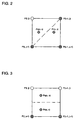
- P(i, j) has a level close to a white peak, and other three pixels P(i+1, j), P(i, j+1) and P(i+1, j+1) have levels close to a black level. Since the pixel P(i, j) in this case has an isolated level, a video has a skew edge component.
- the coefficient Co11 to be sent to the multiplier 11 to which the pixel P(i+1, j+1) is input is set to 0.5
- the coefficient Co00 to be sent to the multiplier 8 to which the pixel P(i, j) is input is set to 1.25
- the coefficient Co10 and the coefficient Co01 to be sent to the multipliers 9 and 10 to which other pixels are input are set to 1.125.
- a pixel Pr(u, v) to be generated is located at a position of ⁇ (i+1)- u ⁇ + ⁇ (j+1)-v ⁇ ⁇ 1 will be explained.
- the coefficient Co00 to be sent to the multiplier 8 to which the pixel P(i, j) is input is set to 0.5
- the coefficient Co11 to be sent to the multiplier 11 to which the pixel P(i+1, j+1) located at a diagonal position is input is set to 1.25
- the coefficient Co10 and the coefficient Co01 to be sent to the multipliers 9 and 10 to which other pixels are input are set to 1.125.
- any one of the above-described two coefficients may be used.
- a longitudinal edge is formed, in which pixels P(i, j) and P(i+1, j) have levels close to a white peak, and P(i, j+1) and P(i+1, j+1) have levels close to a black level.
- a pixel Pr(u, v) to be generated is located at a position of ⁇ (j+1)-v ⁇ ⁇ 0.5 as shown in Fig. 3, the coefficients Co00 and Co10 to be sent to the multipliers 8 and 9 to which P(i, j) and P(i+1, j) are input are set to 0.5, and the coefficients Co01 and Co11 to be sent to the multipliers 9 and 11 to which other two pixels are input are set to 1.5.
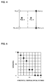
- a transversal edge is formed, in which pixels P(i, j) and P(i, j+1) have levels close to a white peak level, and P(i+1, j) and P(i+1, j+1) have levels close to a black level.
- a pixel Pr(u, v) to be generated is located at a position of ⁇ (i+1)-u) ⁇ ⁇ 0.5 as shown in Fig. 4, the coefficients Co00 and Co01 to be sent to the multipliers 8 and 10 to which the pixels P(i, j) and P(i, j+1) are input are set to 0.5, and the coefficients Co10 and Co11 to be sent to the multipliers 9 and 11 to which other two pixels are input are set to 1.5.
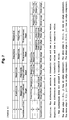
- Fig. 7 is a table 1.
- the "positive” in Table 1 means that a difference value between pixels exceeds a threshold value having a high level, which is set in the edge detecting circuit 7, for example, 64 in case that a video signal is A/D-converted into eight bits, and means that it has a positive value.
- the "negative” in the Table means that it exceeds the threshold value having a high level, which is set in the edge detecting circuit 7, and means that it has a negative value.
- the "-" in the Table means that a difference value between pixels does not exceed another threshold value having a low level, which is set in the edge detecting circuit 7, for example, 16 in case that a video signal is A/D-converted into eight bits.
- the present invention by detecting an edge component of a skew edge, a longitudinal edge and a transversal edge from the four pixels adjacent to the pixel to be generated, adaptively changing the weighting of the pixel which can be the cause of damaging an edge component, based on the detected edge and a spatial position of the pixel to be generated, and conducting pixel-conversion, even in case of conducting interpolation in a video including an edge component, interpolation processing can be conducted by a small-scale circuit while an original edge component is maintained.
Landscapes
- Engineering & Computer Science (AREA)
- Physics & Mathematics (AREA)
- General Physics & Mathematics (AREA)
- Theoretical Computer Science (AREA)
- Multimedia (AREA)
- Signal Processing (AREA)
- Image Processing (AREA)
- Facsimile Image Signal Circuits (AREA)
- Picture Signal Circuits (AREA)
Abstract
Description
Claims (12)
- A pixel interpolation method comprising steps of:detecting existence of an edge component of an image from four pixels adjacent to a pixel to be newly generated by means of interpolation, and in case that the edge component exists, further detecting that the edge component is which kind of edge component out of a skew edge, a longitudinal edge and a transversal edge;selecting weighting coefficients to the adjacent four pixels so that they become small for a pixel which can be the cause of damaging the edge component, from a spatial position relation of said pixel to be generated for the adjacent four pixels and the kind of the detected edge component;multiplying pixel values of the adjacent four pixels by the respective selected coefficients; andconducting pixel-conversion of said pixel to be generated by applying a bilinear interpolation method to said multiplied result.
- A pixel interpolation method according to claim 1,
wherein said step of detecting existence of an edge component determines that the adjacent four pixels have skew edges in case that a difference of levels between certain one pixel and other three pixels exceeds a first threshold value of a high value, and a difference of levels between other three pixels is less than a second threshold value of a low value, and determines that the adjacent four pixels have longitudinal edges if a level difference between the pixels in a horizontal direction is less than the second threshold value, and a level difference between the pixels in a vertical direction exceeds the first threshold value, and determines that the adjacent four pixels have transversal edges if a level difference between the pixels in a vertical direction is less than the second threshold value, and a level difference between the pixels in a horizontal direction exceeds the first threshold value. - A pixel interpolation method according to claim 1,
wherein said spatial position relation of said four pixels is obtained a spatial position relation in a horizontal direction and a vertical direction of the adjacent four pixels and the pixel to be generated from a horizontal synchronizing signal and a horizontal expansion rate, and a vertical synchronizing signal and a vertical expansion rate. - A pixel interpolation method comprising steps of:detecting existence of an edge component of an image from four pixels adjacent to a pixel to be newly generated by means of interpolation, and in case that the edge component exists, further detecting that the edge component is which kind of edge component out of a skew edge, a longitudinal edge and a transversal edge;generating weighting coefficients to the adjacent four pixels so that they become small for a pixel which can be the cause of damaging the edge component, from a spatial position relation of said pixel to be generated for the adjacent four pixels and the kind of the detected edge component, by using a look-up table for showing a relation between a spatial position relation of the pixel to be generated and the weighting coefficients; andconducting pixel-conversion of said pixel to be generated by realizing a bilinear interpolation method by means of the look-up table, and combining the look-up table for conducting the bilinear interpolation and the look-up table of said coefficient generating circuit into one look-up table.
- A pixel interpolation method according to claim 4,
wherein said step of detecting existence of an edge component determines that the adjacent four pixels have skew edges in case that a difference of levels between certain one pixel and other three pixels exceeds a first threshold value of a high value, and a difference of levels between other three pixels is less than a second threshold value of a low value, and determines that the adjacent four pixels have longitudinal edges if a level difference between the pixels in a horizontal direction is less than the second threshold value, and a level difference between the pixels in a vertical direction exceeds the first threshold value, and determines that the adjacent four pixels have transversal edges if a level difference between the pixels in a vertical direction is less than the second threshold value, and a level difference between the pixels in a horizontal direction exceeds the first threshold value. - A pixel interpolation method according to claim 4,
wherein said spatial position relation of said four pixels is obtained a spatial position relation in a horizontal direction and a vertical direction of the adjacent four pixels and the pixel to be generated from a horizontal synchronizing signal and a horizontal expansion rate, and a vertical synchronizing signal and a vertical expansion rate. - A pixel interpolation circuit comprising:an edge detecting circuit for obtaining a difference of levels between two pixels of four pixels adjacent to a pixel to be newly generated by means of interpolation, detecting existence of an edge component, and in case that the edge component exists, detecting that the edge component is which kind of edge component out of a skew edge, a longitudinal edge and a transversal edge;a position detecting circuit for obtaining a spatial position relation of said pixel to be generated for said adjacent four pixels;a coefficient generating circuit for generating weighting coefficients to the adjacent four pixels so that they become small for a pixel which can be the cause of damaging the edge component, from a spatial position relation of said pixel to be generated for the adjacent four pixels and the kind of the detected edge component;a multiplier for multiplying pixel values of the adjacent four pixels by the respective selected coefficients; anda pixel converting circuit for conducting pixel-conversion of said pixel to be generated by applying a bilinear interpolation method to said multiplied result.
- A pixel interpolation circuit according to claim 7,
wherein said edge detecting circuit determines that the adjacent four pixels have skew edges in case that a difference of levels between certain one pixel and other three pixels exceeds a first threshold value of a high value, and a difference of levels between other three pixels is less than a second threshold value of a low value, and determines that the adjacent four pixels have longitudinal edges if a level difference between the pixels in a horizontal direction is less than the second threshold value, and a level difference between the pixels in a vertical direction exceeds the first threshold value, and determines that the adjacent four pixels have transversal edges if a level difference between the pixels in a vertical direction is less than the second threshold value, and a level difference between the pixels in a horizontal direction exceeds the first threshold value. - A pixel interpolation circuit according to claims 7,
wherein said position detecting circuit obtains a spatial position relation in a horizontal direction and a vertical direction of the adjacent four pixels and the pixel to be generated from a horizontal synchronizing signal and a horizontal expansion rate, and a vertical synchronizing signal and a vertical expansion rate. - A pixel interpolation circuit comprising:an edge detecting circuit for obtaining a difference of levels between two pixels of four pixels adjacent to a pixel to be newly generated, detecting existence of an edge component, and in case that the edge component exists, detecting that the edge component is which kind of edge component out of a skew edge, a longitudinal edge and a transversal edge;a position detecting circuit for obtaining a spatial position relation of said pixel to be generated for said adjacent four pixels;a coefficient generating circuit for generating weighting coefficients to the adjacent four pixels so that they become small for a pixel which can be the cause of damaging the edge component, from a spatial position relation of said pixel to be generated for the adjacent four pixels and the kind of the detected edge component, by using a look-up table for showing a relation between a spatial position relation of the pixel to be generated and the weighting coefficients; anda pixel converting circuit for conducting pixel-conversion of said pixel to be generated by realizing a bilinear interpolation method by means of the look-up table, and combining the look-up table for conducting the bilinear interpolation and the look-up table of said coefficient generating circuit into one look-up table.
- A pixel interpolation circuit according to claim 10,
wherein said edge detecting circuit determines that the adjacent four pixels have skew edges in case that a difference of levels between certain one pixel and other three pixels exceeds a first threshold value of a high value, and a difference of levels between other three pixels is less than a second threshold value of a low value, and determines that the adjacent four pixels have longitudinal edges if a level difference between the pixels in a horizontal direction is less than the second threshold value, and a level difference between the pixels in a vertical direction exceeds the first threshold value, and determines that the adjacent four pixels have transversal edges if a level difference between the pixels in a vertical direction is less than the second threshold value, and a level difference between the pixels in a horizontal direction exceeds the first threshold value. - A pixel interpolation circuit according to claims 10, wherein said position detecting circuit obtains a spatial position relation in a horizontal direction and a vertical direction of the adjacent four pixels and the pixel to be generated from a horizontal synchronizing signal and a horizontal expansion rate, and a vertical synchronizing signal and a vertical expansion rate.
Applications Claiming Priority (2)
| Application Number | Priority Date | Filing Date | Title |
|---|---|---|---|
| JP17709799 | 1999-06-23 | ||
| JP11177097A JP2001008037A (en) | 1999-06-23 | 1999-06-23 | Pixel interpolation method and circuit |
Publications (3)
| Publication Number | Publication Date |
|---|---|
| EP1067774A2 true EP1067774A2 (en) | 2001-01-10 |
| EP1067774A3 EP1067774A3 (en) | 2003-10-15 |
| EP1067774B1 EP1067774B1 (en) | 2004-11-10 |
Family
ID=16025096
Family Applications (1)
| Application Number | Title | Priority Date | Filing Date |
|---|---|---|---|
| EP20000112971 Expired - Lifetime EP1067774B1 (en) | 1999-06-23 | 2000-06-20 | Pixel interpolation method and circuit |
Country Status (3)
| Country | Link |
|---|---|
| EP (1) | EP1067774B1 (en) |
| JP (1) | JP2001008037A (en) |
| DE (1) | DE60015659T2 (en) |
Cited By (10)
| Publication number | Priority date | Publication date | Assignee | Title |
|---|---|---|---|---|
| US7391920B2 (en) | 2003-11-04 | 2008-06-24 | Fujifilm Corporation | Image processing method, apparatus, and program |
| US7826686B2 (en) | 2005-03-18 | 2010-11-02 | Seiko Epson Corporation | Pixel interpolation apparatus and pixel interpolation program product |
| WO2011014633A3 (en) * | 2009-07-29 | 2011-05-05 | Qualcomm Incorporated | Method and device for pixel interpolation |
| CN101900538B (en) * | 2009-05-26 | 2012-02-08 | 哈尔滨理工大学 | Dual-four-lead-six interpolation method for depth image of structured light fringe sampling data |
| US8248662B2 (en) | 2007-05-11 | 2012-08-21 | Samsung Electronics Co., Ltd. | Image forming apparatus and method thereof |
| CN103034975A (en) * | 2012-12-18 | 2013-04-10 | 广州杰赛科技股份有限公司 | Image processing method and device |
| US8624938B2 (en) | 2008-12-19 | 2014-01-07 | Semiconductor Energy Laboratory Co., Ltd. | Method for driving liquid crystal display device |
| US8780034B2 (en) | 2009-04-08 | 2014-07-15 | Semiconductor Energy Laboratory Co., Ltd. | Method for driving semiconductor device including super-resolution processing |
| US8970638B2 (en) | 2009-02-06 | 2015-03-03 | Semiconductor Energy Laboratory Co., Ltd. | Method for driving display device |
| US9020303B2 (en) | 2011-02-21 | 2015-04-28 | Mitsubishi Electric Corporation | Image magnification device and method |
Families Citing this family (6)
| Publication number | Priority date | Publication date | Assignee | Title |
|---|---|---|---|---|
| JP4734952B2 (en) * | 2005-02-21 | 2011-07-27 | ヤマハ株式会社 | Image processing method and apparatus |
| JP4703504B2 (en) | 2006-07-21 | 2011-06-15 | ソニー株式会社 | Image processing apparatus, image processing method, and program |
| US20080068173A1 (en) * | 2006-09-13 | 2008-03-20 | Sensormatic Electronics Corporation | Radio frequency identification (RFID) system for item level inventory |
| JP2010141863A (en) * | 2008-12-12 | 2010-06-24 | Pixela Corp | Image processing method, apparatus and program |
| JP5274379B2 (en) * | 2009-06-04 | 2013-08-28 | キヤノン株式会社 | Resolution conversion apparatus and control method thereof |
| JP5478200B2 (en) * | 2009-11-09 | 2014-04-23 | 京セラ株式会社 | Image processing apparatus, image processing method, and image processing program |
Family Cites Families (3)
| Publication number | Priority date | Publication date | Assignee | Title |
|---|---|---|---|---|
| US5054100A (en) * | 1989-11-16 | 1991-10-01 | Eastman Kodak Company | Pixel interpolator with edge sharpening |
| KR950006776B1 (en) * | 1993-01-14 | 1995-06-22 | 삼성전자주식회사 | Interpolation method and circuit of digital image data |
| JP3599435B2 (en) * | 1995-08-09 | 2004-12-08 | 富士写真フイルム株式会社 | Image data interpolation calculation method and apparatus |
-
1999
- 1999-06-23 JP JP11177097A patent/JP2001008037A/en active Pending
-
2000
- 2000-06-20 EP EP20000112971 patent/EP1067774B1/en not_active Expired - Lifetime
- 2000-06-20 DE DE2000615659 patent/DE60015659T2/en not_active Expired - Fee Related
Cited By (30)
| Publication number | Priority date | Publication date | Assignee | Title |
|---|---|---|---|---|
| US7391920B2 (en) | 2003-11-04 | 2008-06-24 | Fujifilm Corporation | Image processing method, apparatus, and program |
| US7826686B2 (en) | 2005-03-18 | 2010-11-02 | Seiko Epson Corporation | Pixel interpolation apparatus and pixel interpolation program product |
| US8248662B2 (en) | 2007-05-11 | 2012-08-21 | Samsung Electronics Co., Ltd. | Image forming apparatus and method thereof |
| US10254586B2 (en) | 2008-12-19 | 2019-04-09 | Semiconductor Energy Laboratory Co., Ltd. | Method for driving liquid crystal display device |
| US11899311B2 (en) | 2008-12-19 | 2024-02-13 | Semiconductor Energy Laboratory Co., Ltd. | Method for driving liquid crystal display device |
| US11300832B2 (en) | 2008-12-19 | 2022-04-12 | Semiconductor Energy Laboratory Co., Ltd. | Method for driving liquid crystal display device |
| US9280937B2 (en) | 2008-12-19 | 2016-03-08 | Semiconductor Energy Laboratory Co., Ltd. | Method for driving liquid crystal display device |
| US8624938B2 (en) | 2008-12-19 | 2014-01-07 | Semiconductor Energy Laboratory Co., Ltd. | Method for driving liquid crystal display device |
| US10578920B2 (en) | 2008-12-19 | 2020-03-03 | Semiconductor Energy Laboratory Co., Ltd. | Method for driving liquid crystal display device |
| US8928706B2 (en) | 2008-12-19 | 2015-01-06 | Semiconductor Energy Laboratory Co., Ltd. | Method for driving liquid crystal display device |
| US10018872B2 (en) | 2008-12-19 | 2018-07-10 | Semiconductor Energy Laboratory Co., Ltd. | Method for driving liquid crystal display device |
| US11837180B2 (en) | 2009-02-06 | 2023-12-05 | Semiconductor Energy Laboratory Co., Ltd. | Method for driving display device |
| US8970638B2 (en) | 2009-02-06 | 2015-03-03 | Semiconductor Energy Laboratory Co., Ltd. | Method for driving display device |
| US10943549B2 (en) | 2009-02-06 | 2021-03-09 | Semiconductor Energy Laboratory Co., Ltd. | Method for driving display device |
| US9583060B2 (en) | 2009-02-06 | 2017-02-28 | Semiconductor Energy Laboratory Co., Ltd. | Method for driving display device |
| US9343018B2 (en) | 2009-04-08 | 2016-05-17 | Semiconductor Energy Laboratory Co., Ltd. | Method for driving a liquid crystal display device at higher resolution |
| US9978320B2 (en) | 2009-04-08 | 2018-05-22 | Semiconductor Energy Laboratory Co., Ltd. | Method for driving semiconductor device |
| US8780034B2 (en) | 2009-04-08 | 2014-07-15 | Semiconductor Energy Laboratory Co., Ltd. | Method for driving semiconductor device including super-resolution processing |
| US10657910B2 (en) | 2009-04-08 | 2020-05-19 | Semiconductor Energy Laboratory Co., Ltd. | Method for driving semiconductor device |
| US12080254B2 (en) | 2009-04-08 | 2024-09-03 | Semiconductor Energy Laboratory Co., Ltd. | Method for driving semiconductor device |
| US11030966B2 (en) | 2009-04-08 | 2021-06-08 | Semiconductor Energy Laboratory Co., Ltd. | Method for driving semiconductor device |
| US11450291B2 (en) | 2009-04-08 | 2022-09-20 | Semiconductor Energy Laboratory Co., Ltd. | Method for driving semiconductor device |
| US11670251B2 (en) | 2009-04-08 | 2023-06-06 | Semiconductor Energy Laboratory Co., Ltd. | Method for driving semiconductor device |
| CN101900538B (en) * | 2009-05-26 | 2012-02-08 | 哈尔滨理工大学 | Dual-four-lead-six interpolation method for depth image of structured light fringe sampling data |
| WO2011014633A3 (en) * | 2009-07-29 | 2011-05-05 | Qualcomm Incorporated | Method and device for pixel interpolation |
| US9129409B2 (en) | 2009-07-29 | 2015-09-08 | Qualcomm Incorporated | System and method of compressing video content |
| CN102484710B (en) * | 2009-07-29 | 2016-10-26 | 高通股份有限公司 | Systems and methods for pixel interpolation |
| CN102484710A (en) * | 2009-07-29 | 2012-05-30 | 高通股份有限公司 | System and method for pixel interpolation |
| US9020303B2 (en) | 2011-02-21 | 2015-04-28 | Mitsubishi Electric Corporation | Image magnification device and method |
| CN103034975A (en) * | 2012-12-18 | 2013-04-10 | 广州杰赛科技股份有限公司 | Image processing method and device |
Also Published As
| Publication number | Publication date |
|---|---|
| EP1067774B1 (en) | 2004-11-10 |
| EP1067774A3 (en) | 2003-10-15 |
| DE60015659T2 (en) | 2005-12-22 |
| JP2001008037A (en) | 2001-01-12 |
| DE60015659D1 (en) | 2004-12-16 |
Similar Documents
| Publication | Publication Date | Title |
|---|---|---|
| EP1067774B1 (en) | Pixel interpolation method and circuit | |
| EP0641508B1 (en) | Method and apparatus for enhancing sharpness of a sequence of images subject to continuous zoom | |
| US6628330B1 (en) | Color interpolator and horizontal/vertical edge enhancer using two line buffer and alternating even/odd filters for digital camera | |
| US7142239B2 (en) | Apparatus and method for processing output from image sensor | |
| EP0639029A2 (en) | Apparatus for converting frame format of television signal | |
| EP0794513A1 (en) | Method and enhancing image using quantized mean-separate histogram equalization and a circuit therefor | |
| US5068722A (en) | Motion vector estimating apparatus | |
| US7679676B2 (en) | Spatial signal conversion | |
| EP0523924A2 (en) | Image signal processing apparatus | |
| US6356310B1 (en) | Signal converting apparatus and method for converting a first digital picture into a second digital picture having a greater number of pixels than the first digital picture | |
| JP3084189B2 (en) | Imaging device | |
| JP3271101B2 (en) | Digital image signal processing apparatus and processing method | |
| KR100298327B1 (en) | Method and Apparatus for high speed Convolution | |
| US5936681A (en) | Video display monitor employing image interpolation | |
| US7006148B2 (en) | Scan line conversion circuit for simultaneously carrying out three-dimensional motion adaptive sequential scan conversion and scan line conversion | |
| US6215525B1 (en) | Scanning line interpolation apparatus and method | |
| US20070258653A1 (en) | Unit for and Method of Image Conversion | |
| JP5045119B2 (en) | Color transient correction device | |
| JPS60130989A (en) | High resolution television receiver | |
| EP0863665B1 (en) | Video display monitor | |
| JPH11196382A (en) | Field interpolation method and circuit | |
| JP2845376B2 (en) | Pixel density converter | |
| JP2752287B2 (en) | Video signal processing circuit | |
| JP2000115720A (en) | Scanning line interpolation device and scanning line interpolation method | |
| JP2833669B2 (en) | Pixel density conversion method |
Legal Events
| Date | Code | Title | Description |
|---|---|---|---|
| PUAI | Public reference made under article 153(3) epc to a published international application that has entered the european phase |
Free format text: ORIGINAL CODE: 0009012 |
|
| AK | Designated contracting states |
Kind code of ref document: A2 Designated state(s): AT BE CH CY DE DK ES FI FR GB GR IE IT LI LU MC NL PT SE |
|
| AX | Request for extension of the european patent |
Free format text: AL;LT;LV;MK;RO;SI |
|
| PUAL | Search report despatched |
Free format text: ORIGINAL CODE: 0009013 |
|
| AK | Designated contracting states |
Kind code of ref document: A3 Designated state(s): AT BE CH CY DE DK ES FI FR GB GR IE IT LI LU MC NL PT SE |
|
| AX | Request for extension of the european patent |
Extension state: AL LT LV MK RO SI |
|
| RIC1 | Information provided on ipc code assigned before grant |
Ipc: 7H 04N 1/40 A Ipc: 7G 06T 3/40 B Ipc: 7H 04N 5/208 B Ipc: 7H 04N 5/14 B |
|
| GRAP | Despatch of communication of intention to grant a patent |
Free format text: ORIGINAL CODE: EPIDOSNIGR1 |
|
| 17P | Request for examination filed |
Effective date: 20040319 |
|
| AKX | Designation fees paid |
Designated state(s): DE FR |
|
| GRAS | Grant fee paid |
Free format text: ORIGINAL CODE: EPIDOSNIGR3 |
|
| GRAA | (expected) grant |
Free format text: ORIGINAL CODE: 0009210 |
|
| AK | Designated contracting states |
Kind code of ref document: B1 Designated state(s): DE FR |
|
| RAP2 | Party data changed (patent owner data changed or rights of a patent transferred) |
Owner name: NEC PLASMA DISPLAY CORPORATION |
|
| REG | Reference to a national code |
Ref country code: IE Ref legal event code: FG4D |
|
| REF | Corresponds to: |
Ref document number: 60015659 Country of ref document: DE Date of ref document: 20041216 Kind code of ref document: P |
|
| RAP2 | Party data changed (patent owner data changed or rights of a patent transferred) |
Owner name: PIONEER PLASMA DISPLAY CORPORATION |
|
| REG | Reference to a national code |
Ref country code: FR Ref legal event code: CD |
|
| RAP2 | Party data changed (patent owner data changed or rights of a patent transferred) |
Owner name: PIONEER CORPORATION |
|
| PLBE | No opposition filed within time limit |
Free format text: ORIGINAL CODE: 0009261 |
|
| STAA | Information on the status of an ep patent application or granted ep patent |
Free format text: STATUS: NO OPPOSITION FILED WITHIN TIME LIMIT |
|
| 26N | No opposition filed |
Effective date: 20050811 |
|
| ET | Fr: translation filed | ||
| REG | Reference to a national code |
Ref country code: FR Ref legal event code: D6 |
|
| REG | Reference to a national code |
Ref country code: FR Ref legal event code: TP |
|
| PGFP | Annual fee paid to national office [announced via postgrant information from national office to epo] |
Ref country code: FR Payment date: 20060621 Year of fee payment: 7 |
|
| PGFP | Annual fee paid to national office [announced via postgrant information from national office to epo] |
Ref country code: DE Payment date: 20060831 Year of fee payment: 7 |
|
| REG | Reference to a national code |
Ref country code: FR Ref legal event code: ST Effective date: 20080229 |
|
| PG25 | Lapsed in a contracting state [announced via postgrant information from national office to epo] |
Ref country code: DE Free format text: LAPSE BECAUSE OF NON-PAYMENT OF DUE FEES Effective date: 20080101 |
|
| PG25 | Lapsed in a contracting state [announced via postgrant information from national office to epo] |
Ref country code: FR Free format text: LAPSE BECAUSE OF NON-PAYMENT OF DUE FEES Effective date: 20070702 |