EP1067621A2 - Nonreciprocal device and communication device using the same - Google Patents
Nonreciprocal device and communication device using the same Download PDFInfo
- Publication number
- EP1067621A2 EP1067621A2 EP00113923A EP00113923A EP1067621A2 EP 1067621 A2 EP1067621 A2 EP 1067621A2 EP 00113923 A EP00113923 A EP 00113923A EP 00113923 A EP00113923 A EP 00113923A EP 1067621 A2 EP1067621 A2 EP 1067621A2
- Authority
- EP
- European Patent Office
- Prior art keywords
- casing
- lower yoke
- terminals
- isolator
- ground terminal
- Prior art date
- Legal status (The legal status is an assumption and is not a legal conclusion. Google has not performed a legal analysis and makes no representation as to the accuracy of the status listed.)
- Granted
Links
- 238000004891 communication Methods 0.000 title claims description 9
- 239000004020 conductor Substances 0.000 claims abstract description 11
- 229910000859 α-Fe Inorganic materials 0.000 claims abstract description 6
- 239000000463 material Substances 0.000 claims description 17
- 229910000679 solder Inorganic materials 0.000 claims description 13
- 230000005540 biological transmission Effects 0.000 claims description 6
- 238000000465 moulding Methods 0.000 claims description 3
- 238000010276 construction Methods 0.000 description 17
- 239000000758 substrate Substances 0.000 description 7
- 239000000696 magnetic material Substances 0.000 description 5
- 238000010586 diagram Methods 0.000 description 4
- 238000000034 method Methods 0.000 description 4
- 230000035939 shock Effects 0.000 description 4
- NINIDFKCEFEMDL-UHFFFAOYSA-N Sulfur Chemical compound [S] NINIDFKCEFEMDL-UHFFFAOYSA-N 0.000 description 3
- 239000003990 capacitor Substances 0.000 description 3
- 238000003780 insertion Methods 0.000 description 3
- 230000037431 insertion Effects 0.000 description 3
- 230000005855 radiation Effects 0.000 description 3
- 239000011347 resin Substances 0.000 description 3
- 229920005989 resin Polymers 0.000 description 3
- XEEYBQQBJWHFJM-UHFFFAOYSA-N Iron Chemical compound [Fe] XEEYBQQBJWHFJM-UHFFFAOYSA-N 0.000 description 2
- 238000005476 soldering Methods 0.000 description 2
- 230000015572 biosynthetic process Effects 0.000 description 1
- 230000007423 decrease Effects 0.000 description 1
- 229910052737 gold Inorganic materials 0.000 description 1
- 229910052742 iron Inorganic materials 0.000 description 1
- 238000004519 manufacturing process Methods 0.000 description 1
- 238000005259 measurement Methods 0.000 description 1
- 229910052759 nickel Inorganic materials 0.000 description 1
- 238000007639 printing Methods 0.000 description 1
- 229910052709 silver Inorganic materials 0.000 description 1
Images


Classifications
-
- H—ELECTRICITY
- H01—ELECTRIC ELEMENTS
- H01P—WAVEGUIDES; RESONATORS, LINES, OR OTHER DEVICES OF THE WAVEGUIDE TYPE
- H01P1/00—Auxiliary devices
- H01P1/32—Non-reciprocal transmission devices
- H01P1/38—Circulators
- H01P1/383—Junction circulators, e.g. Y-circulators
- H01P1/387—Strip line circulators
-
- H—ELECTRICITY
- H01—ELECTRIC ELEMENTS
- H01P—WAVEGUIDES; RESONATORS, LINES, OR OTHER DEVICES OF THE WAVEGUIDE TYPE
- H01P1/00—Auxiliary devices
- H01P1/32—Non-reciprocal transmission devices
-
- Y—GENERAL TAGGING OF NEW TECHNOLOGICAL DEVELOPMENTS; GENERAL TAGGING OF CROSS-SECTIONAL TECHNOLOGIES SPANNING OVER SEVERAL SECTIONS OF THE IPC; TECHNICAL SUBJECTS COVERED BY FORMER USPC CROSS-REFERENCE ART COLLECTIONS [XRACs] AND DIGESTS
- Y10—TECHNICAL SUBJECTS COVERED BY FORMER USPC
- Y10T—TECHNICAL SUBJECTS COVERED BY FORMER US CLASSIFICATION
- Y10T29/00—Metal working
- Y10T29/49—Method of mechanical manufacture
- Y10T29/49002—Electrical device making
- Y10T29/4902—Electromagnet, transformer or inductor
-
- Y—GENERAL TAGGING OF NEW TECHNOLOGICAL DEVELOPMENTS; GENERAL TAGGING OF CROSS-SECTIONAL TECHNOLOGIES SPANNING OVER SEVERAL SECTIONS OF THE IPC; TECHNICAL SUBJECTS COVERED BY FORMER USPC CROSS-REFERENCE ART COLLECTIONS [XRACs] AND DIGESTS
- Y10—TECHNICAL SUBJECTS COVERED BY FORMER USPC
- Y10T—TECHNICAL SUBJECTS COVERED BY FORMER US CLASSIFICATION
- Y10T29/00—Metal working
- Y10T29/49—Method of mechanical manufacture
- Y10T29/49002—Electrical device making
- Y10T29/4902—Electromagnet, transformer or inductor
- Y10T29/49075—Electromagnet, transformer or inductor including permanent magnet or core
-
- Y—GENERAL TAGGING OF NEW TECHNOLOGICAL DEVELOPMENTS; GENERAL TAGGING OF CROSS-SECTIONAL TECHNOLOGIES SPANNING OVER SEVERAL SECTIONS OF THE IPC; TECHNICAL SUBJECTS COVERED BY FORMER USPC CROSS-REFERENCE ART COLLECTIONS [XRACs] AND DIGESTS
- Y10—TECHNICAL SUBJECTS COVERED BY FORMER USPC
- Y10T—TECHNICAL SUBJECTS COVERED BY FORMER US CLASSIFICATION
- Y10T29/00—Metal working
- Y10T29/49—Method of mechanical manufacture
- Y10T29/49002—Electrical device making
- Y10T29/49117—Conductor or circuit manufacturing
- Y10T29/49124—On flat or curved insulated base, e.g., printed circuit, etc.
- Y10T29/49155—Manufacturing circuit on or in base
- Y10T29/49158—Manufacturing circuit on or in base with molding of insulated base
-
- Y—GENERAL TAGGING OF NEW TECHNOLOGICAL DEVELOPMENTS; GENERAL TAGGING OF CROSS-SECTIONAL TECHNOLOGIES SPANNING OVER SEVERAL SECTIONS OF THE IPC; TECHNICAL SUBJECTS COVERED BY FORMER USPC CROSS-REFERENCE ART COLLECTIONS [XRACs] AND DIGESTS
- Y10—TECHNICAL SUBJECTS COVERED BY FORMER USPC
- Y10T—TECHNICAL SUBJECTS COVERED BY FORMER US CLASSIFICATION
- Y10T29/00—Metal working
- Y10T29/49—Method of mechanical manufacture
- Y10T29/49002—Electrical device making
- Y10T29/49117—Conductor or circuit manufacturing
- Y10T29/49174—Assembling terminal to elongated conductor
- Y10T29/49176—Assembling terminal to elongated conductor with molding of electrically insulating material
Definitions
- the present invention relates to a non-reciprocal component, such as a circulator or an isolator, used in a microwave band or the like, and to a communication device using the same.
- a non-reciprocal component such as a circulator or an isolator
- a casing 1 is a box resin casing, which is open at the top face thereof as observed in Fig. 14. Various terminals are provided in this casing 1. In the condition shown in this figure, one input/output (I/O) terminal 2a and ground terminals 3 appear, and an exposed part of another I/O terminal 2b appears inside the casing 1.
- a lower yoke 9 is mounted on the casing 1. Inside the casing 1, capacitors 7a, 7b, and 7c, a chip resistor 8, a ferrite plate 5, line conductors 4a, 4b, and 4c, and a magnetic 6 are placed in this order.
- An upper yoke 10 covers the top face of the casing 1.
- such a conventional isolator has a problem in that when the casing 1 and the lower yoke 9 are assembled by soldering the lower yoke 9 to terminals provided in the casing 1, since a sufficient soldered area thereof cannot be obtained, adequate bonding strength cannot be secured. This may lead to a reduction in reliability of an electronic device. For example, an impact from dropping causes the soldered parts of the electronic device to come off. Furthermore, when the lower yoke 7 and the casing 1 are soldered, there is a risk that since the I/O terminals 2a and 2b and the ground terminals 3 do not form the same plane due to mismatching between the sizes of components on the lower yoke 9 and the sizes of components on the casing 1, some of the terminals may be raised. As a result, when characteristics of this isolator are to be measured, there is a problem in that measurement cannot be performed because terminals of a measuring jig are not properly connected to the I/O terminals 2a and 2b or ground terminals 3.
- a non-reciprocal component that includes a casing having an I/O terminal and a ground terminal formed therein; a ferrite plate, a transmission line conductor, and a magnetic stored in the casing; and an upper yoke and a lower yoke provided at the top face and the bottom face of the casing, respectively.
- the casing is insert-molded with the lower yoke.
- the lower yoke, the I/O terminal, and the ground terminal may be formed by molding a hoop material.
- This construction enables the lower yoke and the casing to be insert-molded in succession, and the lower yoke, the I/O terminal, and the ground terminal to be formed using the same material. Accordingly, the number of parts can be reduced.
- a portion of the lower yoke may be exposed as the ground terminal from the casing. This construction allows the distance between the ground terminal and the lower yoke to be minimized, which minimizes residual inductance.
- the ground terminal is protruded outside the lower yoke, and the ground terminal has a solder resist film formed at the base thereof. Because of this, when mounting is performed on a circuit substrate of an electronic device, solder is prevented from flowing into the bottom face of the lower yoke, which enables soldering to be performed only on terminal parts.
- the thickness of the lower yoke, the thickness of the I/O terminal, and the thickness of the ground terminal are 0.3 mm or less.
- a communication device is provided with a non-reciprocal component according to the first aspect of the present invention.
- the communication device is constructed by providing the non-reciprocal component as a circulator in which a transmission signal and a reception signal are branched.
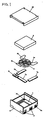
- Fig. 1 is an exploded perspective view of the isolator.
- the isolator is constructed as follows.
- a resin casing 1 is insert-molded along with a lower yoke 9 made of a magnetic material, I/O terminals 2a and 2b, and ground terminals 3.
- the ground terminals 3 are integrated with the lower yoke 9, and the I/O terminals 2a and 2b are insulated from the lower yoke 9.
- Inner ends of the two I/O terminals 2a and 2b are exposed at the inner bottom face of the casing 1.
- capacitors 7a, 7b, and 7c, and a chip resistor 8 of which the top faces and the bottom faces, as observed in the figure, serve as electrode faces are each disposed.
- Transmission line conductors (central conductors) 4a, 4b, and 4c, a ferrite plate 5, and a magnetic 6 are stored in the casing 1 so that the line conductors 4a, 4b, and 4c are held between the ferrite plate 5 and the magnetic 6.
- an upper yoke 10 made of a magnetic material covers an opening of the casing 1.
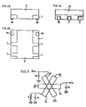
- Figs. 2A, 2B and 2C show three views of the above-described isolator; Fig. 2A is a front view thereof; Fig. 2B is a bottom view thereof; and Fig. 2C is a right-side view thereof.
- Parts of the lower yoke 9 are extended as the four ground terminals 3, and the casing 1 is insert-molded along with the ground terminals 3 and the I/O terminals 2a and 2b. In this manner, by insert-molding the casing 1 along with the lower yoke 9, there is no need to solder the lower yoke 9 to the terminals provided in the casing 1. Accordingly, shock resistance is enhanced.
- the positional accuracy (planar accuracy) of the I/O terminals 2a and 2b and the ground terminals 3 is improved. Therefore, when isolator characteristics are measured, connection failure between a measuring jig and the isolator can be prevented. When the isolator is mounted on a mounting substrate, raising of the terminals can be avoided.
- Fig. 3 is a circuit diagram of the above-described isolator.
- the circuit of the I/O terminals 2a and 2b is constructed as follows.
- the line conductors 4a, 4b, and 4c cross one another so as to establish a mesh connection.
- One end of each of the line conductors is grounded, while the other end thereof and the ground have matching capacitors 7a, 7b, and 7c inserted therebetween.
- the chip resistor 8 is connected as a termination resistor between the non-grounded terminal of the line conductor 4c and the ground. Because of this construction, non-reciprocal property can be obtained between the I/O terminals 2a and 2b.
- a signal passes from the I/O terminal 2a to the I/O terminal 2b with low reflection, whereas a signal that is input to the I/O terminal 2b is hardly output from the I/O terminal 2a due to attenuation in the resistor 8.
- Figs. 4 and 5 show frequency characteristics of the insertion loss of the isolator.
- the solid lines represent characteristics of the isolator according to this embodiment of the present invention, and, for comparison, the dashed-lines represent those of an isolator having a conventional construction.
- the ground terminals 3 are provided as integrally formed portions of the lower yoke 9, the lengths of the ground terminals are minimized, and residual inductance is maintained small, which improves the ground circuit. Consequently, as shown in Fig. 4, low loss is realized and the bandwidth of a characteristic band in which the isolator can be operative is expanded.
- unnecessary radiation decreases, a large amount of attenuation can be obtained in a high frequency region, as shown in Fig. 5.
- ground terminals 3 are provided as integral parts of the lower yoke 9, heat that is generated at the chip resistor 8 functioning as a terminator flows into a ground plane of the mounting substrate via the lower yoke 9 functioning as a ground plate and the ground terminals. Accordingly, heat radiation is improved and electrical power resistant of the isolator is enhanced. Since the operating temperature of the isolator is maintained low due to the radiation, the reliability thereof is increased.
- Figs. 6A, 6B, and 6C show three views of the isolator; Fig. 6A is a front view thereof; Fig. 6B is a bottom view thereof; and Fig. 6C is a right-side view thereof.
- the ground terminals 3 are formed one after another so as to be protruded outside the lower yoke 9.
- Solder resist films 11 are formed by printing or the like at the corresponding bases of these ground terminals apart from the actual operative regions thereof.
- the solder resist films 11 are formed at proximal ends of the ground terminals 3 exposed on an outer bottom surface of the isolator. Otherwise, the construction of the isolator is identical to that shown in the first embodiment.
- solder resist films 11 are located on the bases of the ground terminals 3 extending from the lower yoke 9, when this isolator is mounted on a mounting substrate of an electronic device, solder does not flow into the inner bottom surface of the lower yoke 9 from the ground terminals 3. Accordingly, the I/O terminals 2a and 2b and the ground terminals 3 can be firmly soldered to the mounting substrate.
- Figs. 7A to 7C are illustrations of a process for forming the lower yoke 9 and each of the terminals thereof.
- a hoop material 12 made of a magnetic material obtained by forming a plated film on an iron plate, such as Ag, Ni, Au, or Cu, having a thickness of 0.3 mm or less.
- Sprocket holes 15 are formed so that the hoop material 12 is fed along the longitudinal direction of the hoop material 12.
- the lower yoke 9 is formed by folding the part 9' at the two-dot chain lines shown in Fig. 7A. However, up to this point, the lower yoke 9 still maintains connection with the hoop material 12 via the connecting parts 14.
- the thickness of the hoop material 12 is 0.3 mm or less, it is easy to fold the lower yoke 9 and to cut and raise the cut-and-raised pieces 13a to 13f.
- Fig. 8 illustrates a process that follows the processes shown in Figs. 7A to 7C.
- the casing 1 is insert-molded along with the lower yoke 9 and the cut-and-raised pieces 13a to 13f.
- ends of the cut-and-raised pieces 13c and 13f are exposed as inner terminals of the I/O terminals 2a and 2b at the inner bottom face of the casing 1.
- Ends of the other cut-and-raised pieces 13a, 13b, 13d, and 13e are exposed as inner terminals of the ground terminals 3 at the inner bottom face of the casing 1.
- the cut-and-raised pieces 13a to 13f are cut off along the two-dot chain lines. Parts of the cut-and-raised pieces protruded from the sides of the casing 1 are folded, whereby the I/O terminals 2a and 2b and the ground terminals 3 are formed.
- Figs. 9A, 9B, and 9C show three views of the isolator; Fig. 9A is a front view thereof; Fig. 9B is a bottom view thereof; and Fig. 9C is a right-side view thereof.
- the I/O terminals 2a and 2b, and the ground terminals 3 are formed with the same materials as those of the lower yoke 9. In addition, they are insert-molded with the casing 1. Accordingly, shock resistance is enhanced, and the positional accuracy of the I/O terminals 2a and 2b, and the ground terminals 3 are also enhanced.
- Fig. 10 shows the construction of the hoop material 12 before insert-mold formation of the casing 1.
- the lower yoke 9 made of the magnetic material establishes connection via the connecting parts 14 with frame parts of the hoop material 12 made of the magnetic material.
- the cut-and-raised pieces 13c and 13f are cut and raised from the hoop material 12 and are folded by approximately 180 degrees.
- a resin to be the casing 1 is insert-molded. Then, the connecting parts 14 and the cut-and-raised pieces 13c and 13f are cut off along the two-dot chain lines, and parts of the cut-and-raised pieces protruding from the sides of the casing 1 are folded, whereby the I/O terminals 2a and 2b and the ground terminals 3 are formed.
- Figs. 11A, 11B, and 11C show three views of the isolator constructed by the above-described processes; Fig. 11A is a front view thereof; Fig. 11B is a bottom view thereof; and Fig. 11C is a right-side view thereof. Connecting parts between the lower yoke 9 and the hoop material 12 can be simply used as ground terminals 3.
- Figs. 12A, 12B, and 12C show three views showing the construction of an isolator according to a fifth embodiment of the present invention.
- a solder resist films 11 are formed at the bases of the ground terminals 3. Otherwise, the construction of the isolator is identical to that of the isolator shown in Fig. 11.
- solder resist films 11 By forming the solder resist films 11 at the bases of the ground terminals 3, when this isolator is mounted on the mounting substrate of the electronic device, solder does not flow into the (inner) bottom face of the lower yoke 9 from the ground terminals 3. Accordingly, the I/O terminals 2a and 2b, and the ground terminals 3 are firmly soldered to the mounting substrate.
- Fig. 13 shows a block diagram of the construction of a communication device.
- the two-port isolator is constructed by incorporating the three-port circulator and the terminating resistor therein is shown.
- the three-port circulator can be constructed.
- Port #1 of the circulator constructed in the above-described manner is connected to an output unit of a transmission circuit
- port #2 thereof is connected to an antenna
- port #3 thereof is connected to an input unit of a reception circuit.
- the communication device is constructed, in which the circulator is used as a branching circuit for transmission and reception.
Landscapes
- Non-Reversible Transmitting Devices (AREA)
Abstract
Description
Claims (8)
- A non-reciprocal component comprising:a casing having an input/output terminal and a ground terminal formed therein;a ferrite plate, a transmission line conductor, and a magnetic stored in said casing; andan upper yoke and a lower yoke, provided at the top face and the bottom face of said casing, respectively,
wherein said casing is insert-molded with said lower yoke. - A non-reciprocal component according to Claim 1, wherein, by molding a hoop material, portions of said hoop material define said input/output terminal and said ground terminal.
- A non-reciprocal component according to Claim 1, wherein a portion of said lower yoke is exposed as said ground terminal from said casing.
- A non-reciprocal component according to Claim 2, wherein a portion of said lower yoke is exposed as said ground terminal from said casing.
- A non-reciprocal component according to Claim 3, wherein:said ground terminal is protruded outside said lower yoke; andsaid ground terminal has a solder resist film formed at the base thereof.
- A non-reciprocal component according to claim 4, wherein:said ground terminal is protruded outside said lower yoke; andsaid ground terminal has a solder resist film formed at the base thereof.
- A non-reciprocal component according to Claim 1, wherein the thickness of said lower yoke, the thickness of said input/output terminal, and the thickness of said ground terminal, are each 0.3 mm or less.
- A communication device provided with a non-reciprocal component according to Claim 1.
Applications Claiming Priority (2)
| Application Number | Priority Date | Filing Date | Title |
|---|---|---|---|
| JP18879999 | 1999-07-02 | ||
| JP18879999A JP3356121B2 (en) | 1999-07-02 | 1999-07-02 | Non-reciprocal circuit device and communication device |
Publications (3)
| Publication Number | Publication Date |
|---|---|
| EP1067621A2 true EP1067621A2 (en) | 2001-01-10 |
| EP1067621A3 EP1067621A3 (en) | 2002-05-22 |
| EP1067621B1 EP1067621B1 (en) | 2008-07-02 |
Family
ID=16230016
Family Applications (1)
| Application Number | Title | Priority Date | Filing Date |
|---|---|---|---|
| EP00113923A Expired - Lifetime EP1067621B1 (en) | 1999-07-02 | 2000-06-30 | Nonreciprocal device and communication device using the same |
Country Status (6)
| Country | Link |
|---|---|
| US (2) | US6469588B1 (en) |
| EP (1) | EP1067621B1 (en) |
| JP (1) | JP3356121B2 (en) |
| KR (1) | KR100343321B1 (en) |
| CN (1) | CN1156936C (en) |
| DE (1) | DE60039328D1 (en) |
Cited By (1)
| Publication number | Priority date | Publication date | Assignee | Title |
|---|---|---|---|---|
| GB2368730A (en) * | 2000-05-30 | 2002-05-08 | Murata Manufacturing Co | Method for manufacturing nonreciprocal circuit device |
Families Citing this family (7)
| Publication number | Priority date | Publication date | Assignee | Title |
|---|---|---|---|---|
| JP2002344206A (en) * | 2001-05-11 | 2002-11-29 | Murata Mfg Co Ltd | Non-reciprocal circuit element and communications equipment |
| JP3649162B2 (en) * | 2001-07-06 | 2005-05-18 | 株式会社村田製作所 | Center electrode assembly, non-reciprocal circuit device, communication device, and method of manufacturing center electrode assembly |
| JP3686884B2 (en) * | 2002-06-06 | 2005-08-24 | アルプス電気株式会社 | Manufacturing method of casing for electronic component |
| JP2004312437A (en) * | 2003-04-08 | 2004-11-04 | Alps Electric Co Ltd | Irreversible circuit element, communication device equipment, lead frame for irreversible circuit element, and method of manufacturing irreversible circuit element |
| JP5255577B2 (en) * | 2010-01-13 | 2013-08-07 | 古河電気工業株式会社 | Substrate and substrate manufacturing method |
| CN103403955B (en) * | 2013-01-06 | 2015-07-22 | 华为技术有限公司 | Circulator, isolator and circuit assembly |
| JP7693027B2 (en) * | 2022-01-19 | 2025-06-16 | Astemo株式会社 | Conductor plate manufacturing method, conductive plate assembly |
Family Cites Families (29)
| Publication number | Priority date | Publication date | Assignee | Title |
|---|---|---|---|---|
| JPS5826382A (en) * | 1981-08-07 | 1983-02-16 | Hitachi Ltd | Bubble memory device and its manufacture |
| JP2526219B2 (en) * | 1986-10-23 | 1996-08-21 | 日立フェライト 株式会社 | Lumped constant type circulator and isolator |
| DE3824013C2 (en) | 1988-07-15 | 1997-02-13 | Profor Ab | Method of attaching a packed straw to a package and device for attaching the same |
| JPH03206701A (en) * | 1990-01-08 | 1991-09-10 | Murata Mfg Co Ltd | Manufacture of irreversible circuit element and hoop shaped component |
| US5159294A (en) * | 1990-03-01 | 1992-10-27 | Murata Manufacturing Co., Ltd. | Non-reciprocal circuit element |
| JP2884742B2 (en) * | 1990-08-23 | 1999-04-19 | タカタ株式会社 | Method of manufacturing acceleration sensor |
| JP2501715B2 (en) | 1992-05-18 | 1996-05-29 | 富士通テン株式会社 | Noise control device |
| JP3269141B2 (en) * | 1992-11-25 | 2002-03-25 | 株式会社村田製作所 | Non-reciprocal circuit device |
| JPH06164222A (en) * | 1992-11-25 | 1994-06-10 | Murata Mfg Co Ltd | Microwave magnetic body and production thereof |
| JPH07326907A (en) * | 1994-05-31 | 1995-12-12 | Tokin Corp | Non-reciprocal circuit element |
| JPH088610A (en) | 1994-06-21 | 1996-01-12 | Murata Mfg Co Ltd | Irreversible circuit element |
| JP3399099B2 (en) | 1994-07-27 | 2003-04-21 | 株式会社村田製作所 | Non-reciprocal circuit device |
| JP3206701B2 (en) | 1994-08-31 | 2001-09-10 | 富士電機株式会社 | Manufacturing method of magnetic recording medium |
| JPH08116163A (en) * | 1994-10-18 | 1996-05-07 | Fuji Xerox Co Ltd | Mounting of surface mount component |
| KR0141952B1 (en) * | 1994-12-19 | 1998-06-01 | 문정환 | Semiconductor package and production thereof |
| JPH0955607A (en) | 1995-08-11 | 1997-02-25 | Taiyo Yuden Co Ltd | Irreversible circuit element |
| JP3617134B2 (en) | 1995-08-23 | 2005-02-02 | 松下電器産業株式会社 | Operational electronic components |
| JP3264193B2 (en) * | 1995-11-27 | 2002-03-11 | 株式会社村田製作所 | Non-reciprocal circuit device |
| US5702775A (en) * | 1995-12-26 | 1997-12-30 | Motorola, Inc. | Microelectronic device package and method |
| JP3755068B2 (en) | 1996-05-27 | 2006-03-15 | Tdk株式会社 | Non-reciprocal circuit device and manufacturing method thereof |
| JPH1041706A (en) * | 1996-07-26 | 1998-02-13 | Hitachi Metals Ltd | Irreversible circuit element |
| JPH10107511A (en) | 1996-09-26 | 1998-04-24 | Murata Mfg Co Ltd | Irreversible circuit element |
| JP3303690B2 (en) | 1996-10-29 | 2002-07-22 | 日立金属株式会社 | Non-reciprocal circuit device |
| JPH10290140A (en) | 1997-04-15 | 1998-10-27 | Murata Mfg Co Ltd | Surface acoustic wave device |
| JPH1168411A (en) | 1997-08-08 | 1999-03-09 | Murata Mfg Co Ltd | Non-reversible circuit element |
| JPH1174706A (en) * | 1997-08-27 | 1999-03-16 | Hitachi Metals Ltd | Irreversible circuit element |
| JP3275806B2 (en) * | 1997-12-04 | 2002-04-22 | 株式会社村田製作所 | Non-reciprocal circuit device |
| JP3622639B2 (en) * | 2000-05-30 | 2005-02-23 | 株式会社村田製作所 | Non-reciprocal circuit device manufacturing method |
| JP3649144B2 (en) * | 2001-04-10 | 2005-05-18 | 株式会社村田製作所 | Non-reciprocal circuit element, communication apparatus, and non-reciprocal circuit element manufacturing method |
-
1999
- 1999-07-02 JP JP18879999A patent/JP3356121B2/en not_active Expired - Lifetime
-
2000
- 2000-06-30 US US09/608,157 patent/US6469588B1/en not_active Expired - Lifetime
- 2000-06-30 EP EP00113923A patent/EP1067621B1/en not_active Expired - Lifetime
- 2000-06-30 DE DE60039328T patent/DE60039328D1/en not_active Expired - Lifetime
- 2000-07-03 KR KR1020000037753A patent/KR100343321B1/en not_active Expired - Lifetime
- 2000-07-03 CN CNB001217615A patent/CN1156936C/en not_active Expired - Lifetime
-
2002
- 2002-05-24 US US10/156,318 patent/US6971166B2/en not_active Expired - Lifetime
Cited By (3)
| Publication number | Priority date | Publication date | Assignee | Title |
|---|---|---|---|---|
| GB2368730A (en) * | 2000-05-30 | 2002-05-08 | Murata Manufacturing Co | Method for manufacturing nonreciprocal circuit device |
| GB2368730B (en) * | 2000-05-30 | 2002-10-16 | Murata Manufacturing Co | Method for manufacturing nonreciprocal circuit device |
| US6625869B2 (en) | 2000-05-30 | 2003-09-30 | Murata Manufacturing Co., Ltd. | Method for manufacturing nonreciprocal circuit device |
Also Published As
| Publication number | Publication date |
|---|---|
| DE60039328D1 (en) | 2008-08-14 |
| EP1067621A3 (en) | 2002-05-22 |
| EP1067621B1 (en) | 2008-07-02 |
| CN1282990A (en) | 2001-02-07 |
| KR20010015146A (en) | 2001-02-26 |
| US20020140517A1 (en) | 2002-10-03 |
| KR100343321B1 (en) | 2002-07-10 |
| CN1156936C (en) | 2004-07-07 |
| JP2001024406A (en) | 2001-01-26 |
| US6971166B2 (en) | 2005-12-06 |
| US6469588B1 (en) | 2002-10-22 |
| JP3356121B2 (en) | 2002-12-09 |
Similar Documents
| Publication | Publication Date | Title |
|---|---|---|
| JP3269409B2 (en) | Non-reciprocal circuit device | |
| EP1067621B1 (en) | Nonreciprocal device and communication device using the same | |
| EP0959518A1 (en) | Dielectric filter, dielectric duplexer, and transceiver | |
| US6087905A (en) | Nonreciprocal circuit device having a low-pass filter formed on a spacer | |
| US6882262B2 (en) | Nonreciprocal circuit device and communication device using same | |
| KR100340718B1 (en) | Nonreciprocal Circuit Device And Communication Apparatus Incorporating Same | |
| JP2002344206A (en) | Non-reciprocal circuit element and communications equipment | |
| JP3269141B2 (en) | Non-reciprocal circuit device | |
| US6724276B2 (en) | Non-reciprocal circuit device and communication apparatus | |
| KR100394807B1 (en) | Nonreciprocal circuit device and communication device using same | |
| JP3414355B2 (en) | Non-reciprocal circuit device and communication device | |
| EP1107347A2 (en) | Nonreciprocal circuit device, communication apparatus, and method for manufacturing nonreciprocal circuit device | |
| JP3651137B2 (en) | Non-reciprocal circuit element | |
| US6573809B1 (en) | Dielectric resonator device, dielectric duplexer, and communication apparatus incorporating same | |
| US20040201431A1 (en) | Nonreciprocal circuit element, communication apparatus, lead frame for nonreciprocal circuit element, and method for manufacturing nonreciprocal circuit element | |
| JP4563980B2 (en) | Surface mount type package and semiconductor device | |
| JP2002151913A (en) | Irreversible circuit component and communication unit | |
| JP2000077553A (en) | High frequency package | |
| JP2001111309A (en) | Non-reciprocal circuit element and communication equipment | |
| US20050007207A1 (en) | Nonreciprocal circuit device and telecommunications apparatus including the same |
Legal Events
| Date | Code | Title | Description |
|---|---|---|---|
| PUAI | Public reference made under article 153(3) epc to a published international application that has entered the european phase |
Free format text: ORIGINAL CODE: 0009012 |
|
| 17P | Request for examination filed |
Effective date: 20000630 |
|
| AK | Designated contracting states |
Kind code of ref document: A2 Designated state(s): AT BE CH CY DE DK ES FI FR GB GR IE IT LI LU MC NL PT SE |
|
| AX | Request for extension of the european patent |
Free format text: AL;LT;LV;MK;RO;SI |
|
| PUAL | Search report despatched |
Free format text: ORIGINAL CODE: 0009013 |
|
| AX | Request for extension of the european patent |
Free format text: AL;LT;LV;MK;RO;SI |
|
| AKX | Designation fees paid |
Designated state(s): DE FR GB |
|
| RAP1 | Party data changed (applicant data changed or rights of an application transferred) |
Owner name: MURATA MANUFACTURING CO., LTD. |
|
| GRAP | Despatch of communication of intention to grant a patent |
Free format text: ORIGINAL CODE: EPIDOSNIGR1 |
|
| GRAS | Grant fee paid |
Free format text: ORIGINAL CODE: EPIDOSNIGR3 |
|
| GRAA | (expected) grant |
Free format text: ORIGINAL CODE: 0009210 |
|
| AK | Designated contracting states |
Kind code of ref document: B1 Designated state(s): DE FR GB |
|
| REG | Reference to a national code |
Ref country code: GB Ref legal event code: FG4D |
|
| REF | Corresponds to: |
Ref document number: 60039328 Country of ref document: DE Date of ref document: 20080814 Kind code of ref document: P |
|
| PLBE | No opposition filed within time limit |
Free format text: ORIGINAL CODE: 0009261 |
|
| STAA | Information on the status of an ep patent application or granted ep patent |
Free format text: STATUS: NO OPPOSITION FILED WITHIN TIME LIMIT |
|
| 26N | No opposition filed |
Effective date: 20090403 |
|
| REG | Reference to a national code |
Ref country code: FR Ref legal event code: PLFP Year of fee payment: 17 |
|
| REG | Reference to a national code |
Ref country code: FR Ref legal event code: PLFP Year of fee payment: 18 |
|
| REG | Reference to a national code |
Ref country code: FR Ref legal event code: PLFP Year of fee payment: 19 |
|
| PGFP | Annual fee paid to national office [announced via postgrant information from national office to epo] |
Ref country code: DE Payment date: 20190619 Year of fee payment: 20 |
|
| PGFP | Annual fee paid to national office [announced via postgrant information from national office to epo] |
Ref country code: FR Payment date: 20190619 Year of fee payment: 20 |
|
| PGFP | Annual fee paid to national office [announced via postgrant information from national office to epo] |
Ref country code: GB Payment date: 20190619 Year of fee payment: 20 |
|
| REG | Reference to a national code |
Ref country code: DE Ref legal event code: R071 Ref document number: 60039328 Country of ref document: DE |
|
| REG | Reference to a national code |
Ref country code: GB Ref legal event code: PE20 Expiry date: 20200629 |
|
| PG25 | Lapsed in a contracting state [announced via postgrant information from national office to epo] |
Ref country code: GB Free format text: LAPSE BECAUSE OF EXPIRATION OF PROTECTION Effective date: 20200629 |