EP1065734A2 - Bonding type semiconductor substrate, semiconductor light emitting element, and preparation process thereof. - Google Patents
Bonding type semiconductor substrate, semiconductor light emitting element, and preparation process thereof. Download PDFInfo
- Publication number
- EP1065734A2 EP1065734A2 EP00304862A EP00304862A EP1065734A2 EP 1065734 A2 EP1065734 A2 EP 1065734A2 EP 00304862 A EP00304862 A EP 00304862A EP 00304862 A EP00304862 A EP 00304862A EP 1065734 A2 EP1065734 A2 EP 1065734A2
- Authority
- EP
- European Patent Office
- Prior art keywords
- semiconductor substrate
- layer
- epitaxial growth
- substrate
- light emitting
- Prior art date
- Legal status (The legal status is an assumption and is not a legal conclusion. Google has not performed a legal analysis and makes no representation as to the accuracy of the status listed.)
- Granted
Links
Images







Classifications
-
- H—ELECTRICITY
- H10—SEMICONDUCTOR DEVICES; ELECTRIC SOLID-STATE DEVICES NOT OTHERWISE PROVIDED FOR
- H10H—INORGANIC LIGHT-EMITTING SEMICONDUCTOR DEVICES HAVING POTENTIAL BARRIERS
- H10H20/00—Individual inorganic light-emitting semiconductor devices having potential barriers, e.g. light-emitting diodes [LED]
- H10H20/01—Manufacture or treatment
- H10H20/011—Manufacture or treatment of bodies, e.g. forming semiconductor layers
- H10H20/018—Bonding of wafers
-
- H—ELECTRICITY
- H10—SEMICONDUCTOR DEVICES; ELECTRIC SOLID-STATE DEVICES NOT OTHERWISE PROVIDED FOR
- H10H—INORGANIC LIGHT-EMITTING SEMICONDUCTOR DEVICES HAVING POTENTIAL BARRIERS
- H10H20/00—Individual inorganic light-emitting semiconductor devices having potential barriers, e.g. light-emitting diodes [LED]
- H10H20/80—Constructional details
- H10H20/81—Bodies
- H10H20/814—Bodies having reflecting means, e.g. semiconductor Bragg reflectors
-
- H—ELECTRICITY
- H10—SEMICONDUCTOR DEVICES; ELECTRIC SOLID-STATE DEVICES NOT OTHERWISE PROVIDED FOR
- H10H—INORGANIC LIGHT-EMITTING SEMICONDUCTOR DEVICES HAVING POTENTIAL BARRIERS
- H10H20/00—Individual inorganic light-emitting semiconductor devices having potential barriers, e.g. light-emitting diodes [LED]
- H10H20/80—Constructional details
- H10H20/81—Bodies
- H10H20/817—Bodies characterised by the crystal structures or orientations, e.g. polycrystalline, amorphous or porous
-
- H—ELECTRICITY
- H10—SEMICONDUCTOR DEVICES; ELECTRIC SOLID-STATE DEVICES NOT OTHERWISE PROVIDED FOR
- H10W—GENERIC PACKAGES, INTERCONNECTIONS, CONNECTORS OR OTHER CONSTRUCTIONAL DETAILS OF DEVICES COVERED BY CLASS H10
- H10W72/00—Interconnections or connectors in packages
- H10W72/90—Bond pads, in general
-
- H—ELECTRICITY
- H10—SEMICONDUCTOR DEVICES; ELECTRIC SOLID-STATE DEVICES NOT OTHERWISE PROVIDED FOR
- H10H—INORGANIC LIGHT-EMITTING SEMICONDUCTOR DEVICES HAVING POTENTIAL BARRIERS
- H10H20/00—Individual inorganic light-emitting semiconductor devices having potential barriers, e.g. light-emitting diodes [LED]
- H10H20/80—Constructional details
- H10H20/81—Bodies
- H10H20/819—Bodies characterised by their shape, e.g. curved or truncated substrates
-
- H—ELECTRICITY
- H10—SEMICONDUCTOR DEVICES; ELECTRIC SOLID-STATE DEVICES NOT OTHERWISE PROVIDED FOR
- H10P—GENERIC PROCESSES OR APPARATUS FOR THE MANUFACTURE OR TREATMENT OF DEVICES COVERED BY CLASS H10
- H10P10/00—Bonding of wafers, substrates or parts of devices
- H10P10/12—Bonding of semiconductor wafers or semiconductor substrates to semiconductor wafers or semiconductor substrates
- H10P10/128—Bonding of semiconductor wafers or semiconductor substrates to semiconductor wafers or semiconductor substrates by direct semiconductor to semiconductor bonding
-
- H—ELECTRICITY
- H10—SEMICONDUCTOR DEVICES; ELECTRIC SOLID-STATE DEVICES NOT OTHERWISE PROVIDED FOR
- H10W—GENERIC PACKAGES, INTERCONNECTIONS, CONNECTORS OR OTHER CONSTRUCTIONAL DETAILS OF DEVICES COVERED BY CLASS H10
- H10W72/00—Interconnections or connectors in packages
- H10W72/50—Bond wires
- H10W72/531—Shapes of wire connectors
- H10W72/536—Shapes of wire connectors the connected ends being ball-shaped
-
- H—ELECTRICITY
- H10—SEMICONDUCTOR DEVICES; ELECTRIC SOLID-STATE DEVICES NOT OTHERWISE PROVIDED FOR
- H10W—GENERIC PACKAGES, INTERCONNECTIONS, CONNECTORS OR OTHER CONSTRUCTIONAL DETAILS OF DEVICES COVERED BY CLASS H10
- H10W72/00—Interconnections or connectors in packages
- H10W72/50—Bond wires
- H10W72/59—Bond pads specially adapted therefor
Definitions
- the present invention relates to a bonding type semiconductor substrate and a semiconductor light emitting element, and preparation processes thereof.
- the present invention relates to a bonding type semiconductor substrate based on a novel wafer direct bonding technique, a light emitting element such as LEDs (light emitting diode) with a high brightness obtained by applying the technique, and preparation processes thereof.
- Fig. 22 shows an embodiment of a visible light LED of InGaAlP based on a conventional technique.
- InGaAlP epitaxial growth layers 84, 85, 86 contributing to light emission are formed on an n-type GaAs substrate 82.
- a buffer layer may be disposed between the substrate and the epitaxial growth layer in compliance with required specifications in order to obtain an excellent light emitting layer.
- Electrodes 89 for supplying an electric current are each disposed on the upper surface of the epitaxial growth layer 86 and the lower surface of the substrate 82, respectively.
- a layer for diffusing the electric current or a layer for taking an electric contact is often disposed between an upper electrode 89 and the epitaxial growth layer 86.
- the layer which can emit light by the recombination of carriers is the active layer 85.
- the epitaxial layers 84 and 85 formed on and under the active layer 85 are the cladding layers 84 and 86 having a wider band gap than the active layer in order to confine the carriers and to thereby heighten an emission efficiency.
- the band gap is required to be optimized according to a design for the purpose of adjusting the wavelength of the emission and for the purpose of confining the carriers. Furthermore, it is desirable for a good epitaxial growth that a lattice constant of the epitaxial growth layer matches a lattice constant of the substrate 82. Since InGaAlP which is a group III-V compound contains three elements of In, Ga and Al as components in the group III, the band gap and the lattice constant can be independently designed by selecting a composition ratio of these elements.
- a composition of the epitaxial growth layer is represented by the following formula In x (Ga 1-y Al y ) 1-x P
- the lattice constant of the epitaxial growth layer almost matches that of a GaAs substrate by setting a composition ratio (x) of In to 0.5.
- the wavelength of the emission can be selected within a region of visible light. Furthermore, since the layers can epitaxially grow under the lattice matching condition with a GaAs substrate which is most general as a compound semiconductor substrate, there exist advantages that the substrate is easily available and the epitaxial growth is relatively easy.
- a GaAs substrate has a disadvantage that it absorbs light in a region of visible light. Therefore, part of the light emitted on an InGaAlP epitaxial growth layer is absorbed by GaAs substrate, and hence a brightness of LED decreases unavoidably.
- a material which is transparent in the region of the visible light is preferably employed as a substrate.
- the usual transparent material is GaP, but since the GaP substrate cannot obtain the lattice matching with InGaAlP, the good epitaxial growth is difficult.
- USP 5,376,580 filed in 1993 proposes a method for a wafer bonding between an InGaAlP epitaxial growth layer and a GaP substrate.
- This proposed method comprises removing a GaAs substrate from the epitaxial growth layer, closely bonding a GaP substrate instead of the GaAs substrate, and then carrying out a heat treatment under pressure to integrally bond them.
- the increase of the brightness of LED can be attained.
- the stability and productivity of the wafer bonding step are insufficient, because the epitaxial growth layer after the removal of the GaAs substrate is thin and thus its handling is difficult, and a special apparatus is necessary for the heat treatment under pressure.
- the direct bonding technique comprises mutually closely bonding two substrates having mirror-finished surfaces by themselves at room temperature under a substantially dust-free atmosphere, and then integrally joining them by a heat treatment.
- This technique has an advantage that the whole surface can be joined without leaving any unbonded part, because the whole surfaces are closely bonded to each other prior to the heat treatment. Moreover, it is not necessary to apply a pressure during the heat treatment, any special apparatus or equipment is not required.
- the mechanism of the direct bonding between the Si wafers is understood as follows.
- OH groups are formed on the surface of the wafer by cleaning or washing with water. Then, when the surfaces of the two wafers are contacted with each other, the OH groups attract each other by a hydrogen bond, so that the wafers closely bond at room temperature.
- a bonding power in this case is strong enough to eliminate a usual warp of the wafer, whereby the close bonding all over the surfaces can be achieved.
- a dehydrative condensation Si-OH : HO-Si ⁇ Si-O-Si + H 2 O
- Si-OH HO-Si ⁇ Si-O-Si + H 2 O
- an n-type cladding layer 94, an active layer 95 and a p-type cladding layer 96 are grown on an n-type GaAs substrate 92.
- a GaP substrate 91 is directly bonded to the surface of the epitaxial growth layer 96.
- the GaAs substrate 92 is removed by polishing or etching, and after upside down, electrodes 99 are disposed on the upper surface of the n-type cladding layer 94 and under the lower surface of GaP substrate 91, respectively, so that an InGaAlP-based LED having GaP as the substrate 91 is obtained as shown in Fig. 23D.
- the present invention has been accomplished in view of the above circumstances, and an object of the present invention is to provide a bonding type semiconductor substrate directly, stably and closely bonded all over the surface of an epitaxial growth layer formed on a semiconductor substrate.
- Another object of the present invention is to provide a semiconductor light emitting element.
- Still another object of the present invention is to provide a preparation process of the above substrate.
- a further object of the present invention is to provide a preparation process of the above light emitting element.
- a bonding type semiconductor substrate comprising a first epitaxial growth layer formed on a first semiconductor substrate, and a second semiconductor substrate whose at least one surface is mirror-finished and which is integrally bonded to the first epitaxial growth layer via the mirror-finished surface or a second epitaxial growth layer grown on the mirror-finished surface; a thermal expansion coefficient of the first epitaxial growth layer being close to a thermal expansion coefficient of the second semiconductor substrate.
- the bonding type semiconductor substrate stably and closely bonded can be provided.
- a semiconductor light emitting element comprising:
- the warp of a wafer having the epitaxial growth layer (hereinafter, referred to as "epi-wafer") can be reduced. Accordingly, there can be provided the bonding type semiconductor substrate where even the relatively thick epi-wafer is stably and closely joined to the second semiconductor substrate.
- the first semiconductor substrate is formed from GaAs
- the second semiconductor substrate is formed from Gap
- the epitaxial growth layer is represented by the formula In x (Ga 1-y Al y ) 1-x P.
- a composition ratio in the above composition formula of the first cladding layer is suitably 0.45 ⁇ x ⁇ 0.50 and 0 ⁇ y ⁇ 1.
- a process for preparing a bonding type semiconductor substrate comprising:
- the second semiconductor substrate can be joined to the epitaxial growth layer. Accordingly, the semiconductor substrate can be prepared in a high yield.
- the warp of the epi-wafer can be reduced. Accordingly, the epi-wafer can be stably joined to the second semiconductor substrate, so that the bonding type semiconductor substrate can be prepared in a higher yield.
- the process may further comprising a forth step of subjecting the resultant laminate to a heat treatment after at least part of the surface of said first semiconductor substrate has been removed therefrom.
- the surface part of the first semiconductor substrate is removed prior to the heat treatment, and hence an average thermal expansion coefficient of the whole epi-wafer is much the same as the thermal expansion coefficient of the epitaxial growth layer and is close to the thermal expansion coefficient of the second semiconductor substrate. Accordingly, the breakage of the bonded substrate at the successively repeated heat treatment can be prevented, so that the joining type semiconductor substrate which is more excellent in bonding strength can be prepared in a much higher yield.
- the above first step preferably contains a step of forming a cover layer on the epitaxial growth layer
- the above second step is desirably a step of removing the cover layer by etching. Accordingly, it is unnecessary to directly remove the surface part of the epitaxial growth layer, whereby it becomes possible to precisely control the thickness of the epitaxial growth layer.
- the above first cladding layer is desirably formed by selecting a composition ratio of the mixed crystals so that the lattice constant may match the lattice constant of the first semiconductor substrate.
- the epitaxial growth layer is formed between the first semiconductor substrate and the laminate, and preferably contains a protective film which functions as an etching stopper in the step of removing the first semiconductor substrate.
- This protective film can afford a margin at the time of the etching and can also prevent the evaporation of doped impurities and P (phosphorus) which is a constitutional component of the first cladding layer in the step of the above heat treatment.
- crystals are aligned in a substantially similar direction, and hence a dangling bond and crystal defects can be reduced and the rise of electric resistance can be inhibited.
- a bonding type semiconductor substrate comprising:
- a semiconductor light emitting element comprising a light emitting layer and a substrate having a transparency to emission, wherein
- the first embodiment according to the present invention will be explained.
- the embodiment is the one wherein a bonding type semiconductor substrate according to the present invention is applied to an InGaAlP-based LED.
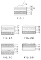
- Fig. 1 is a schematic cross-sectional view showing the InGaAlP-based LED in this embodiment.
- An LED 1 shown in the same drawing comprises a laminate 10 including the epitaxial layers 14-16.
- the laminate 10 may include various structure other than the specific example shown in the firgure.
- the laminate includes an active layer 15, an n-type cladding layer 14 and a p-type cladding layer 16 between which the active layer 15 is interposed; a GaP substrate 11 integrally joined to the lower surface of the laminate; and electrodes 19 formed on the upper surface of the n-type cladding layer and on the lower surface of GaP substrate, respectively.
- the laminate may include other layers such as a contact layer and/or a bonding layer as shown in Fig. 16 afterwards.
- the laminate 10 is formed by epitaxially growing mixed crystals of a compound semiconductor using GaAs substrate as a substrate for growth which is not shown in the drawing.
- the GaP substrate 11 is directly bonded closely and joined at room temperature, the main surface defined as the surface to be joined to the cladding layer 16 being mirror-finished, and the laminate 10 being left as it is formed on the substrate for growth.
- the substrate for growth is removed after the close bonding and joining.
- All of the active layer 15 and two cladding layers 14 and 16 can be represented by the above-mentioned formula 1).
- each composition is suitably selected so as to obtain a lattice matching the substrate for growth, especially at room temperature, warp of the substrate for growth is remarkably reduced and, as a result, it is enabled to join the GaP substrate 11 to the laminate 10 over the whole surfaces.
- the GaP substrate 11 for p-type one has diameter of 2 inches and thickness of 250 ⁇ m
- LED 1 of the present embodiment is formed on the GaP substrate which does not absorb the light in the region of visible light, it can emit light of high brightness.
- emitting property of the LED 1 is evaluated, it is confirmed that its brightness is more than twice as high as that of LED 100.
- the first example of process for preparing a bonding type semiconductor substrate according to the present invention is explained with reference to Fig. 2.
- the present example solves the problem of particle attachment to the surface of the epitaxial growth layer formed on the first semiconductor substrate, and the characteristic points are to form a cover layer on the surface of the epi-wafer, and to remove particles attached to the epi-wafer together with the cover layer prior to direct bonding of the second semiconductor substrate to the epi-wafer.
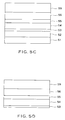
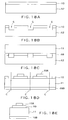
- Figs. 2A to 2D are rough cross sections illustrating a process according to the present example. In Fig. 2, the top and bottom in Fig. 1 is reversed.
- the epi-wafer for direct bonding is formed by laminating a buffer layer 18 on an n-type GaAs substrate 12, an n-type cladding layer 14, an active layer 15, a p-type cladding layer 16 and a surface cover layer 17, successively.
- These epitaxial growth layers are formed according to, for example, MOCVD (Metal Organic Chemical Vapor Deposition) method.
- the n-type GaAs substrate 12 has a size of diameter of 2 inches and thickness of 250 ⁇ m, is doped with Si as impurity in a carrier concentration of about 1E18/cm 3 , and its main surface is mirror-finished.
- the buffer layer 18 is composed of GaAs, the thickness being 0.5 ⁇ m.
- Uppermost layer of the surface cover layer 17 is made of GaAs and the thickness is 0.1 ⁇ m.
- etching was conducted by dipping the epi-wafer into a mixture of 8 parts by volume of sulfuric acid, 1 part by volume of aqueous hydrogen peroxide and 1 part by volume of water to remove the surface cover layer 17 as shown in Fig. 2B.
- the mixture selectively etches the GaAs cover layer.
- the epi-wafer from which the surface cover layer 17 was removed was directly bonded to a GaP substrate 11 to obtain a bonded substrate shown in Fig. 2C.
- a GaP substrate 11 was washed with a surfactant, dipped in dilute hydrofluoric acid to remove native oxide on the surface, and dried with a spinner after washing with water.
- the epi-wafer was, after the surface cover layer 17 had been removed according to the above-mentioned method, subjected to a treatment with dilute hydrofluoric acid in a similar manner as the above GaP substrate 11 case to remove oxide, followed by washing with water and drying with a spinner. All these pre-treatments were conducted under a clean atmosphere in a clean room.
- the epi-wafer subjected to the pre-treatment was placed so that the epitaxial layer may become the upper surface
- the GaP substrate 11 was placed on the epi-wafer so that the mirror-finished surface may become the lower surface, and they were closely bonded at room temperature. Since the GaP is transparent, the bonding conditions can be observed by eye.
- the GaP substrate 11 was placed on the epi-wafer, the central part of the GaP substrate 11 closely bonded first since the epi-wafer warped convexly in a front view.
- the closely bonded part spontaneously expanded to the peripheral part of the GaP substrate 11 only upon standing, and then, whole part of the GaP substrate closely bonded within 1 minute except for the peripheral chamfered part.
- the substrates closely bonded at room temperature were stood up in line in a quartz boat and subjected to a heat treatment in a diffusion furnace.
- the bonded substrates were divided into two groups consisting of 5 pieces each, and one group was treated at 800°C and the other at 400°C.
- the treating time was 1 hour in both cases and the atmosphere was argon containing 10% hydrogen.
- 3 pieces of the 5 pieces treated at 800°C were broken or cracked on the epi-wafer side.
- 5 pieces treated at 400°C remained without breakage or crack.
- Such a difference in accordance to the temperature at the heat treatment is due to the breakage of the bonded substrate which is resulted in by the thermal stress generated at the heat treatment of the room-temperature-bonded substrate at a high temperature because of the difference of thermal expansion coefficient between the epi-wafer of which substrate is GaAs and the GaP substrate. Since the difference of thermal expansion at temperature elevation and the difference of thermal contraction at temperature decrease are lowered in proportion to the temperature in the case of a low treating temperature, the breakage did not occur during the heat treatment at 400°C.
- the GaAs substrate 12 of the epi-wafer was removed as shown in Fig. 2D.
- the step of removing the GaAs substrate 12 was accomplished by dipping the bonded substrate into a mixture of ammonia and aqueous hydrogen peroxide, followed by selective etching of GaAs. The etching also removed the GaAs buffer layer 18 at the same time.
- LED 1 shown in Fig. 1 was obtained by placing the electrodes 19 at the GaP substrate 11 and the n-type cladding layer 14.
- the first example of the semiconductor light emitting element according to the present invention was explained in the above mainly regarding the steps of removing the GaAs cover layer on InGaAlP epitaxial growth layer by selective etching until the bonding.
- the entire cover layer is not necessarily removed and removal of only a part of the layer from its surface may be allowed as long as the similar effect is obtained.
- a surface part of the epitaxial layer to be bonded may be removed without placing the cover layer.
- the cover layer was placed and completely removed by selective etching in order to control the thickness precisely.
- the process for removing the surface particles of the present example is effective not only at the direct bonding between the above-mentioned InGaAlP epitaxial growth layer and GaP substrate but also at wafer bonding to an epitaxial growth layer.
- the method of the bonding is not limited to the above-mentioned method, and the process for removing the surface particles of the present example is also applicable to a method of subjecting to a heat treatment under loading a weight, a bonding method with applying a voltage, and a bonding method using a bonding layer or a material for bonding.
- the following explains second example of preparing a closely bonded semiconductor substrate according to the present invention.
- the present example solves the problem of insufficient bonding at room temperature in the step of the direct bonding by adjusting a lattice constant of InGaAlP material.
- the rest procedure is much the same as in the first example.
- the present example is also illustrated as a concrete example applied to a preparation of LED 1 with reference to rough cross section of Fig. 2.
- the characteristic of the present example is to reduce the warp of the epi-wafer by adjusting the lattice constant without changing the properties affecting the emission such as a band gap, with utilizing the properties of an InGaAlP material.
- the InGaAlP material is mixed crystals of InP, GaP and AlP. According to the principle generally called the Vegard's law, the lattice constant and the band gap of mixed crystals becomes an averaged value in accordance to the composition ratio of the lattice constants and the band gaps of the substances composing the mixed crystals.
- composition ratios x and y in the formula 1) composition ratios of InP, GaP and AlP calculated from these x and y, and the lattice constant and the band gap calculated from the composition ratios according to the Vegard's law.
- the lattice constant the ratio to the lattice constant of GaAs that is 0.56533 nm is also shown.
- Nos. 1, 2, and 3 are the cases of InP, AlP, and GaP, respectively, and the values of the column are employed for the calculation of the lattice constant and the band gap.
- the columns of Nos. 4 and 5 show the composition of the epi-wafer with which close bonding at room temperature was impossible as explained in the first example of the process for preparing a bonding type semiconductor substrate according to the present invention.
- the columns of Nos. 6 to 9 show the compositions of conventional red LED and green LED explained in the part of Background Art.
- the conventional red LED and green LED all the lattice constants are larger than that of GaAs, and this fact is the reason for occurrence of warp of the epi-wafer.
- a lattice constant of an epitaxial growth layer was matched with that of the substrate at a high temperature at which epitaxial growth was conducted. This aims to reduce lattice strain and thus to obtain a high quality epitaxial growth layer.
- the lattice constant is matched at a high temperature, since thermal expansion coefficient of an epitaxial growth layer is generally different from that of the substrate, the lattice constants becomes mismatched upon cooling to room temperature at the bonding step which resulted in occurrence of the warp.
- the present invention is characterized by reduced warp of the epi-wafer with considering the lattice matching as important for realizing direct bonding.
- the concrete means are as follows.
- the columns of Nos. 10 to 19 show changes of the lattice constant as In composition of the cladding layer is reduced from the original value of the epi-wafer (No. 5) with which close bonding at room temperature is failed.
- x 0.47
- the lattice constant becomes the same as that of GaAs.
- x below 0.47
- the lattice constant becomes smaller than that of GaAs, and as a result, a stress acts on the wafer to warp the wafer concavely.
- an epi-wafer was prepared by way of trial by changing only the composition of the cladding layer and subjected to direct bonding test. As the value of x was lowered, the warp of the epi-wafer decreased.
- the present example is not limited to the direct bonding between InGaAlP epitaxial growth layer and GaP wafer but also provides similar effects even when applied to the other wafer bonding.
- the following explains third example of preparing a closely bonded semiconductor substrate according to the present invention.
- the present example solves the problem of breakage resulted in from the difference of thermal expansion between wafers to be directly bonded.
- the breakage of the substrates at direct bonding is prevented by lowering the temperature of a heat treatment to 400°C. Since the thermal expansion occurs roughly in proportion to the treating temperature, lowering the treating temperature donates to prevent the breakage of the substrates. On the other hand, lowering the treating temperature causes a possibility of incomplete bonding owing to an insufficient migration and rearrangement of atoms at bonding interface. Since a process for preparing a bonding type semiconductor substrate is applied to a preparation of LED in the present example, it is required that joining strength is enough at LED preparing processes and electric current can be applied across the bonding interface. In the first example, the joining strength obtained through the heat treatment at 400°C was found to be enough for preparing LED according to the present invention.
- VF voltage VF was measured when a constant current of 20 mmA was applied in normal direction.
- a GaAs contact layer was placed between the cladding layer and the electrode using an etching layer shown in Fig. 4.
- VF of those treated at 800°C was 2.0 V on average and 2.1 V at maximum and was the same as that of the conventional LED.
- VF of the LEDs treated at 400°C was 2.1 V on average which was almost the same, but 3.2 V at maximum. The large value shows presence of insufficient part at direct bonding. The result of the measurement suggests that perfection of bonding is sometimes not compatible with decrease of difference of thermal expansion between the wafers by lowering the treating temperature.
- Fig. 4A shows an epi-wafer to be used in the process of the present example.
- the epi-wafer is different from the epi-wafer shown in Fig. 2A at the point that an etching-stopping layer 33 is formed between a GaAs layer 38 and an GaAs substrate 32, the rest being substantially the same.
- the etching-stopping layer 33 is made of InAlP having a thickness of 0.2 ⁇ m.
- a GaP wafer mentioned below substantially the same one as in the first example is used.
- the GaAs substrate was removed prior to the heat treatment.
- This point is the characteristic of the present invention.
- the closely bonded substrate shown in Fig. 4C was dipped in a mixture of ammonia and aqueous hydrogen peroxide to remove the GaAs substrate 32 by etching. Since the etching solution does not etch InAlP, after the etching, the etching-stopping layer 33 remains as shown in Fig. 4D.
- the treating temperature was 800°C that was a higher one of the two temperatures used in the first example.
- the etching-stopping layer 33 was removed, as shown in Fig. 4 E, by etching it with a mixture of phosphoric acid, aqueous hydrogen peroxide, and water.
- the GaAs layer 38 was removed by etching it with a mixture of sulfuric acid, aqueous hydrogen peroxide, and water, a part of which was still remained.
- LED 2 shown in Fig. 4F was obtained by placing the electrodes 39 on the lower surface of the GaP substrate 31 and on the upper side of the n-type cladding layer 34 where the GaAs layer 38 was remained. The remaining GaAs layer 38 acts as a contact layer.
- any of the five pieces of the bonded substrate was not broken and no crack was observed in the present example, though three of the five pieces were broken in the first example.
- both of the brightness and VF were the same as those prepared from the bonded substrate which was not broken at the heat treatment at 800°C among the bonded substrate of the first example.
- the reason for avoiding the breakage of the bonded substrate at the heat treatment resulted in from removal of the GaAs substrate 32 of the epi-wafer prior to the heat treatment is as follows. Namely, the breakage of the bonded substrate is due to the difference between the thermal expansion coefficient of the epi-wafer and that of the GaP substrate 31. Since the volume of the epi-wafer is mostly composed of the GaAs substrate 32, average thermal expansion coefficient is almost equal to that of GaAs. Since GaAs has larger thermal coefficient than GaP has, average thermal expansion coefficient of the epi-wafer is also larger than that of the GaP substrate 31.
- the epitaxial growth layer side of the epi-wafer warps convexly, though the lattice constant of the epitaxial growth layer is matched with the GaAs substrate 32.
- This fact means that the thermal expansion coefficient of the epitaxial growth layer is smaller than that of the GaAs substrate 32. Therefore, when the GaAs substrate 32 is removed from the epi-wafer, average thermal expansion coefficient of the epi-wafer becomes that of the epitaxial growth layer which is close to that of the GaP substrate 31. As the result, the breakage of the bonded substrate does not occur even when it is subjected to the heat treatment. Accordingly, without removal of the entire GaAs substrate 32 prior to the heat treatment, average thermal expansion coefficient of the epi-wafer comes close to the GaP substrate 31, and thereby the breakage of the bonded substrate is prevented.
- the etching-stopping layer 33 is utilized so that the n-type cladding layer 34 may not be exposed during the heat treatment. This aims to prevent the possibility of evaporation of P (phosphorus) having a high vapor pressure upon heating an InGaAlP material at a high temperature, so called phosphorus-escape. It is desirable not to expose the epitaxial growth layer participating directly the emission of the active layer and cladding layer during the heat treatment.
- Japanese Patent No. 2801672 a method which comprises subjecting to the heat treatment at a low temperature, making one of the wafers thin, and then subjecting to the heat treatment at a high temperature.
- This method includes, by making one wafer thin, reducing thermal stress added to another wafer, and does not relates to reduction of thermal stress through changing the average thermal expansion coefficient of the whole epi-wafer.
- the heat treatment is conducted at a low temperature to obtain a predetermined bonding strength, and an epitaxial wafer substrate is subsequently removed, followed by the heat treatment at a predetermined high temperature.
- the low-temperature heat treatment is preferably conducted at a low temperature of 100 to 300°C or lower. This reason is as follows. As the dehydrogenation/condensation reaction proceeds, the bonding strength increases, but at the same time, the amount of desorbed water content also increases.
- This embodiment is characterized in that a high performance LED can be realized by sandwiching a light emitting body with two transparent substrates and by bonding them so that the bowing or cracking of the wafer is prevented certainly and easily.
- Figs. 5A through 5F exemplarily show the process for fabricating a green light emitting element according to the embodiment.
- a n-type GaAs layer 52 having a thickness of about 0.5 ⁇ m is grown on the GaAs substrate 51 having a thickness of about 250 ⁇ m.
- the n-type cap layer 58 and p-type etching-stop layer 57 are etched and the p-type cladding layer 56 is exposed. Then the native oxide and the particles (not shown) on the surface of the cladding layer 56 are removed. The native oxide and the particles on the surface of the p-type transparent substrate (GaP substrate) 59, which is shown in Fig. 5C, are also removed. The substrate 59 is prepared in a separate process from the light emitting body.
- the p-type transparent substrate 59 having a thickness of 250 ⁇ m, for example, is placed on the surface of the cladding layer 56 in a close contact at room temperature.
- the GaAs substrate 51 and the GaAs layer 52 are removed by an appropriate etching process.
- n-type transparent substrate (GaP substrate) 60 which is shown in Fig. 5E, are removed.
- This substrate 60 is also prepared in a separate process from the light emitting body.
- the n-type transparent substrate 60 having a thickness of 250 ⁇ m, for example, is placed on the surface of the layer 53 in a close contact at room temperature.
- the substrate 59 and the layer 56 as well as the substrate 60 and the layer 53 are bonded at a high temperature by heating up to 800 °C , for example, in a flow of argon (Ar) gas. Then the wafer is cooled down to the room temperature.
- the bonding temperature is not limited to the specific temperature of 800 °C, and the temperature may preferably in a range of 500-1200 °C.
- a transparent electrode 62 made of ITO (a mixture of indium oxide and tin oxide) is formed.
- the substrate temperature may preferably be at room temperature (around 22 °C) and the ratio of the flow rate of argon and oxygen be around 100:1, for example, and the total pressure may preferably be set around 1 ⁇ 10 -3 Torr.
- AuBe gold-beryllium
- the wafer is then annealed at 450 °C for 15 minutes, for example.
- the wafer is then scribed into LED chips. These chips are encapsulated in a resin mold package, for example. Thus, the fabrication process of the light emitting element according to the embodiment is completed.
- Figs. 6A through 6G show the comparative process for fabricating a green light emitting element, which the inventors have conducted.
- an etching-stop layer 132 is grown on the GaAs substrate 131. Then, a p-type cladding layer 133, an active layer 134, a n-type cladding layer 135, a cap layer 136 are grown in this sequence. Thus, the light emitting body is formed by the epitaxial growth.
- the cap layer 136 is etched and the n-type cladding layer 135 is exposed.
- a n-type transparent supporting layer 137 having a thickness of 10-50 ⁇ m is epitaxially grown on the surface of the cladding layer 135.
- the GaAs substrate 131 is removed and the etching-stop layer 132 is exposed by an appropriate etching process.
- the etching-stop layer 132 is removed by an appropriate etching technique and the cladding layer 133 is exposed.
- a p-type transparent substrate 138 having a thickness of about 250 ⁇ m is bonded onto the cladding layer 33 by pressing them at high temperature.
- a metal electrode 139 is formed on the supporting layer 137, and a metal electrode 140 is formed on the surface of the substrate 138.
- the fabrication process of the comparative light emitting element is completed.
- the substrate is need to be bonded by pressing them at high temperature in order to obtain a good ohmic contact at the interface between the p-type cladding layer 133 and the transparent substrate 138.
- the epitaxially grown supporting layer 137 is considerably thinner than the substrate 138, the stress due to the difference of the thermal expansion between the cladding layer 135 and the supporting layer 137 becomes smaller than the stress between the cladding layer 133 and the substrate 138.
- the stresses at the upper and lower sides of the wafer do not balance.
- the wafer bows as exemplarily shown in Fig. 7, and the cracks 143 occur.
- the emission characteristics of the LED degrades remarkably.
- the supporting layer 137 is grown as thick as the substrate 138, the above-explained problem may be solved. However, that is an unrealistic solution since it takes enormous long time to grow such a thick layer by an epitxial growth technique.
- the light emitting devices comprising a bonded structure can be successfully obtained without any bowing or cracks.
- the transparent substrate 59 is bonded to the cladding layer 56 and the substrate which is made of the same material and has the same thickness as the substrate 60 is bonded to the cladding layer 54 via the layer 53.
- the substrates 59 and 60 are made of the same material and have a essentially same thickness.
- Fig. 8 shows the measured emission intensities taken from the light emitting body of the LED before and after bonding the substrates 59 and 60 in the third embodiment of the present invention. As shown in the figure, the emission intensity does not decrease and the performance of the LED is kept even after the bonding process.
- the temperature in a range of 500-1200 °C during the bonding in order to obtain the good ohmic contact at the interface between the light emitting body and the substrates 59 and 60.
- the light emitting body is sandwiched by the two substrates 59 and 60, it takes much shorter time to fabricate the structure as compared to the comparative example where the supporting layer 137 needs to be epitaxially grown for a long time.
- the substrates 59 and 60 can be quite easily made thicker, up to about 250 ⁇ m for example, without a need for a long-lasting epitaxial growth.
- the side surfaces of these substrate become broader.
- the output intensity of the LED can be increased because the broad side surfaces of the substrates reflect the light from the light emitting body toward the emission surface of the LED.
- the invention is not limited in the specific example.
- the invention can also be useful for light emitting devices having a emission wavelength other than green band.
- the transparent substrates usable in the present invention are not limited to the GaP substrate.
- Other substrates usable are, for example, the ones conductive and transparent enough at the desired wavelength (the preferred transparency may be larger than 90%) such as a GaN substrate.
- This embodiment is characterized in that two wafers are aligned at their bonding so that from a crystallographic viewpoint, "the back side" of one wafer may be joined to "the top side” of the other wafer.
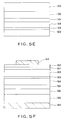
- Fig. 9 is a schematic view explaining how to bond substrates according to this embodiment.
- the semiconductor substrates are usually obtained by slicing off a single crystalline ingot exemplified in Fig. 9A in a predetermined crystal orientation.
- the respective top surfaces 11A and 11 of the wafers 111 and 112 obtained by slicing off the ingot IG are mirror-polished, and an epitaxial layer or the like is then formed on the mirror-polished surfaces, if necessary. Afterward, the two wafers are bonded to each other, with the respective top sides 11A and 112A facing to each other.
- the interface does not have the electric resistance, as far as the carrier concentration of the bonding faces is set to a high level and a heat treatment temperature for the bonding is selected in an appropriate range. For example, even when a (111) face is bonded to a (100) face, the interface resistance is not present, if the wafers with the (100) face is rotated 45 degrees with respect to each other.
- the wafer 111 is bonded to the wafer 112 in such a manner that the former wafer's back side face 111B may face to the latter wafer's top side face 112A.
- the Inventor has found that, as mentioned later, such an bonding method improves the crystallinity of the bonding interface and largely reduces an electrical resistant component.
- a monochrystalline ingot IG grown in a [100] direction has two directions of one in which a (111) A face appears and the other in which a (111) B face, both faces being inclined with respect to its grow axis.
- the (111) A face here refers, for example, an atomic plane in which group-III elements appear on the top side dominantly and the (111) B face, an atomic plane in which group-V elements do so.
- the top sides of the semiconductor substrates 111 and 112 obtained by slicing that monocrystalline ingot at a predetermined angle with respect to its (111) A face become faces 111A and 112A respectively on which the physical properties of the (111) A face appear dominantly. While their back sides 111B and 112B, on the other hand, become those on which the physical properties of the (111) B face appear dominantly.
- the crystal is inclined when it is sliced off is that it is convenient in epitaxial growth with a substrate having an inclined top side orientation than with a so-called “just" orientation type substrate, so that in general, the (100) face is inclined in a (111) face direction.
- such compound semiconductors as GaAs or GaP
- the side of the (100) face inclined in the (111) group III face direction has (100) faces and (111) faces in mixture and has a higher proportion of group III atoms, while the side inclined in the (111) group V face direction, on the other hand, has a high proportion of group V atoms. Conversely, the face inclined in the (111) group V face has a higher proportion of group V atoms.
- two semiconductor substrates to be bonded to each other are of the same material, preferably they have approximately the same inclination angle of the top side. With this, a best balance is provided between the group III and group V atoms.
- the top side inclination angle is also adjusted, taking into consideration their physical properties. This is because different materials may have different proportions of group III and group V atoms with respect to the inclination angle.
- the back side and the top side can be bonded to obtain effects.
- the (100) face has conventionally been considered to be electrically equivalent on both the back side and the top side.
- group III and group V compound semiconductors such as GaAs and GaP have a zing blende structure and their group III and group V atoms arranged at their respective face-centered cubic lattice positions different from each other in such a configuration that the respective lattices are shifted from each other by 1/4 a lattice constant in a diagonal direction.
- This embodiment provide almost the same remarkable effects even when two semiconductor substrates sliced off from different ingots are bonded to each other.
- Fig. 10 is a concept diagram showing how to bond two semiconductor substrates sliced off from two different ingots.
- a semiconductor substrate 11 having an off-angle inclined in the (111) direction is sliced off from a GaP monochrystalline ingot grown in the [100] direction.
- the semiconductor substrate 11 has a top side 11A on which the (111) A face component appears dominantly and a back side 11B on which the (111) B face component appears dominantly.
- a semiconductor substrate 12 sliced off with an off-angle from the GaAs ingot also has a top side 12A on which the (111) A face component appears dominantly and a back side 12B on which the (111) B face component appears dominantly.
- the back side 11B and the top side 12A face to each other in bonding. Also, the top side 11A and the back side 12B are bonded to each other.
- a good balance between the group-III and group-V atoms can be obtained at the interface, thereby decreasing the number of the dangling bonds and the crystal defects as well as largely reducing the electric resistance.
- the top side and “the back side” of semiconductor substrates sliced off from different monocrystalline ingots can be made on the basis of its direction with respect to direction of growing the ingot, i.e. the seed crystal. That is to say, when an ingot is grown generally, the crystal orientation of the seed crystal is set constant. Therefore, even with different ingots, their (111) A face or (111) B face direction has a constant relationship with respect to the growing direction. That is to say, even for two semiconductor substrates sliced off from mutually different ingots, the side of both of them which is nearer to the seed crystal may be defined to be “the top side” face and the opposite side, to be “the back side” face, to thereby bond each other.
- a typical compound semiconductor wafer commercially available often has at a portion thereof a straight cutting, refereed to as "an index flat (IF)". With this, "the top side” and “the back side” of a wafer can be easily identified.
- IF index flat
- the top side and “the back side” of semiconductor substrates sliced off from different ingots can also be decided by mesa etching. That is to say, a GaAs or GaP wafer, when subjected to mesa etching, would have a forward mesa and a backward mesa of its cross-sectional geometry which intersect with each other at a right angle. Also, between the top and back sides of each wafer thus etched, their forward mesas go orthogonal. The direction of these forward and backward mesas appears corresponding to the orientation of the respective (111) A and (111) B faces of the crystal. Therefore, based on these forward mesa and backward mesa directions, the top and back sides of the semiconductor substrate can be discriminated from each other.
- the Gap wafers 111 and 112 were sliced off as inclined 15 degrees in the (111) direction from the GaP monocrystalline ingot grown in the ⁇ 100 ⁇ direction.
- sliced off wafers 111 and 112 were classified into two groups in such a way that the first group of the wafers were, as shown in Fig. 9B, polished on the upper faces (top sides) 11A and 112A to provide a mirror face) and the other group of wafers were, as shown in Fig. 9C, polished on the lower faces (back sides) 111B of the wafers 111 and the upper faces (top sides) 112A of the wafer 112.
- These wafers with the polished top side have their polished faces inclined in the (111) Ga face direction, while the wafers with the polished back side face their polished faces inclined in the (111) P face direction.
- GaP substrates were bonded by a method detailed later using the heat treatment at 800°C.
- a GaP epitaxial layer with a changed carrier concentration was grown on the GaP face to be bonded.
- the thus bonded wafer was divided to the bonding face with an electrode provided on both sides thereof into dice with a size of 250 ⁇ m ⁇ , to measure the I-V characteristics in order to obtain a resistance at the interface by subtracting a bulk resistance of the GaP substrate.
- Fig. 11 is a graph showing a relationship between the carrier concentration at the bonding face and the interface resistance.
- a black circle represents a wafer with the top sides bonded to each other
- a white triangle represents a wafer with the top and back sides bonded to each other.
- the wafer with the top sides bonded to each other (represented by the black circle) exhibits the decreasing interface resistance with the increasing carrier concentration although that resistance is not reduced to zero.
- the wafer with the top and back sides bonded to each other (represented by the while triangle) according to the present invention exhibits a very low interface resistance even with a low carrier concentration, so that the interface resistance was successfully reduced to zero when the carrier concentration was raised to around 2 x 10 18 cm -3 .
- the relationship between the carrier concentration and the interface resistance stays almost the same even without the epitaxial layer on the top side, so that by using a substrate with a higher carrier concentration, the interface resistance can be lowered even with no epitaxial layer.
- GaAs wafer 12 was prepared as inclined 15 degrees in the (111) Ga face direction, on which was epitaxial-grown as shown in Fig. 2A, LED structures 18-17 made of InGaAlP.
- the bonding face (top side of a p-type cladding layer 16) of thus obtained quarternary epitaxial wafer is inclined 15 degrees in the (111) Ga face direction like the substrate.
- GaP wafers 11 two GaP wafers inclined 15 degrees in the (111) Ga face direction were prepared, with one of them having its top side polished and the other having its back side polished.
- the GaAs substrate 12 was removed, to check the operating voltage of thus obtained LED.
- the operating voltage was 4.5V of the LED when electrified with 20 mA which had the bonding face of the GaP wafer 11 inclined in the (111) Ga face direction like the GaAs substrate 12.
- the operating voltage was remarkably lowered to 2V of the LED when electrified with 20 mA which had the bonding face of the GaP wafer 11 inclined in the (111) P face direction according to the present embodiment, exhibiting a distinct decrease in the interface resistance.
- wafers having a (100) just top side orientation were sliced off from an GaP monocrystalline ingot, with its face near to the ingot's seed crystal being defined as the top side.
- these wafers were mirror-polished on their top side or back side, on which mirror face was epitaxial-grown a GaP layer with a carrier concentration of 1 ⁇ 10 18 cm -3 to a thickness of 0.2 ⁇ m.
- the carrier concentration of the epitaxial GaP layer was relatively low is that as mentioned with respect to Fig. 11, the lower carrier concentration provides a larger influence of the combination of the bonding faces on the interface resistance and hence relatively easier comparison.
- the wafers were bonded to each other with their respective top sides or their top and back sides facing each other, to measure the interface resistance.
- the combination with the respective top sides bonded to each other exhibited no Ohmic properties of the current-voltage characteristics at the interface, with a voltage of about 2.2V being generated near the interface when it is electrified with a current of 20 mA.
- the combination with the top and back sides bonded to each other exhibited a straight-line-like Ohmic property of its current-voltage characteristics, with a small voltage of 0.8V when it is electrified with a current of 20 mA.
- each wafer has its own “top side” and “back side” corresponding to the growing direction of the ingot, so that by bonding "the top side” and the back side” to each other, the interface resistance can be reduced significantly.
- This embodiment features applying a pressure not to the whole but only part of each of two wafers when bonded to each other, thus relaxing "a shift" due to thermal expansion.
- Fig. 12 is a schematic diagram explaining this embodiment. That is to say, the Inventor discussed uniquely how to hold and pressurize the two wafers A and B when they are bonded to each other according to any of the preceding embodiments.
- Figs. 12A and 12B show how to pressure and hod the wafers according to this embodiment, while Figs. 12C and 12D explain a pressuring/holding method as a comparison example.
- the two wafers A and B are put on a sufficiently large jig J3 as superposed one on the other, with no load applied from the above.
- the wafers A and B can be freely expanded in the in-plane direction S, so that there occurs no problems of cracking due to a difference in the thermal expansion coefficient, although the bonding may often be insufficient.
- the two wafers A and B are held on sufficiently large jigs J3 and J4 respectively and pressured by a load P.
- the wafers A and B cannot easily be expanded in the in-plane direction, so that "a shift" due to a difference in the thermal expansion coefficient cannot be absorbed and relaxed, thus resulting in wafer cracking in some cases.
- the two wafers A and B are not wholly pressured but only respective parts of them are pressed by the load P by use of jigs J1 and J2 arranged face to face. If the wafers A and B are made of different materials, "a shift" occurs due to a difference in the thermal expansion coefficient when they are heated. According to this embodiment, however, only part of the wafers can be held and pressured, to permit the other parts other than the pressured parts to be easily expanded and contracted in the in-plane direction. Resultantly, "the shift" due to the difference in the thermal expansion coefficient can be tolerated in bonding.
- the wafer B is held wholly by the jig J3 but pressed only partly by the load P from the jig J1 above the wafer A.
- the wafers A and B can be expanded and contracted in the in-plane direction, thus absorbing and relaxing "the shift" due to a difference in the thermal expansion coefficient.
- Figs. 13A to 13D are schematic cross-sectional views specifically explaining how to perform this embodiment.
- n-type GaAs substrate 12 of epitaxial wafers to be directly bonded to each other are sequentially formed in a laminate a buffer layer 18, an n-type cladding layer 14, an active layer 15, a p-type cladding layer 16, and a top-side cover layer 17.
- These epitaxial-grown layers are formed by e.g. a MOCVD (Metal Organic Chemical Vapor Deposition) method.
- the n-type GaAs substrate 12 with a diameter of two inches and a thickness of 250 ⁇ m, has an impurity of Si doped to a carrier concentration of about 1 ⁇ 10 18 cm/cm 3 and also has its main face mirror-polished.
- the buffer layer 18 is made of GaAs, having a thickness of 0.5 ⁇ m.
- the top layer, the top-side cover layer 17 is two-layer structured, with the lower layer being a 0.1- ⁇ m thick GaAs layer 17A and the upper layer being a 0.2- ⁇ m thick InGaAlP layer 17B.
- the epitaxial wafer was immersed in a mixture of ammonia and a hydrogen peroxide solution to remove a deposit on its back side and washed with an interfacial active agent, to subsequently etched etch the cover layer 17B made of InGaAlP using a phosphoric acid at 70°C. This etching process was selectively stopped at the underlying GaAs layer 17A.
- the epitaxial wafer was immersed in a mixture solution consisting by volume of one part of ammonia and 15 parts of hydrogen peroxide solution to be etched, thus removing the underlying GaAs cover layer 17A as sown in Fig. 13B. This mixture solution was used to selectively etch the GaAs cover layer 17A, exhibiting actually that the top-side cover layer 17A was removed in a few seconds, to completely expose the p-type cladding layer 16 in one minute of immersion.
- the GaP substrate 11 was washed with an interfacial active agent and immersed in a dilute hydrofluoric acid to remove its natural oxide film, washed with water, and then dried with a spinner.
- the epitaxial wafer had its top-side cover layer 17 removed by the above-mentioned method and then was subjected to a dilute hydrofluoric acid to remove the oxide film, washed with water, and then dried with a spinner like the GaP substrate 11.
- the epitaxial wafer ad the GaP substrate 11 may of course be adjusted in their crystal orientation so that their top and back sides may be bonded properly.
- the epitaxial wafer as finished of the pretreatment was placed with its epitaxial-grown layer facing upward, on which was placed the GaP substrate 11 with its mirror face facing downward, so that they were bonded tightly at room temperature.
- GaP is transparent, so that the tightly bonded state can be observed by visual inspection. Since the epitaxial wafer, when the GaP substrate 11 was placed thereon, was warped in a convex as viewed from the front, the GaP substrate 11 was bonded tight first at its middle. Only left as is, the tightly bonded portion of the GaP substrate 11 naturally spread to its periphery and, in one minute, that substrate was whole bonded tightly except chamfers at its periphery. This step was repeated to bond a total of 15 couples of the wafers at room temperature.
- the wafer couple thus bonded at room temperature was placed in a diffusion furnace and subjected to a heat treatment for 800°C.
- the atmosphere employed was of argon containing 10% of hydrogen.
- the bonded couples were classified into three groups each consisting of five couples and compared simultaneously using different heat treatment jigs.
- the substrates tightly bonded to each other were sandwiched vertically by carbon plates having each a 5- ⁇ m-diameter circular protrusion at the center thereof, on which was placed a 120-gram carbon-made weight to press only the middle thereof.
- These five jigs were all capable of bonding the whole surface of the wafers, thus avoiding wafer cracks.
- the wafers couple was placed on a flat carbon plate and, with no load placed thereon, subjected to the heat treatment.
- This method came up with a large peel-off portion in excess of 30% in area over two of the five couples. No wafer cracks were observed.
- the wafer couple was sandwiched between flat carbon plates and, with a weight placed thereon, subjected to the heat treatment.
- two of the five couples exhibited cracks and the remaining three came short of complete bonding.
- All the wafers including those with cracks had their periphery bonded but their middle peeled off, which may be considered because the periphery which was thicker due to irregularities in the wafer thickness was bonded first, so that a shift at the interface caused by thermal expansion could not be absorbed.
- this embodiment came up with a confirmation that by partially holding and pressuring the wafers, the bonding process can be conducted at a high yield.
- the semiconductor light emitting element related to this embodiment can typically be formed using the substrate bonding technologies mentioned above with reference to the first through fourth embodiments.
- Fig. 14A is a concept diagram showing a cross-sectional configuration of the LED related to the embodiment
- Fig. 14B is a concept diagram showing that of a conventional LED given as a comparison example.
- both of the LEDs each comprise a GaP substrate 11, which has thereon a cladding layer 14, an active layer 15, and a cladding layer 16 and also which is sandwiched by an upper electrode 19A and a lower electrode 19B.
- a contact layer a current-bottleneck layer, or a current-spread layer.
- the conventional LED has the active layer 15 and the transparent substrate equal to each other in size and also equal in area as viewed from the above.
- Such a conventional LED can be prepared by cutting or cleaving a wafer having many LEDs thereon into many dice of the LED chip.
- the laminate 10 including the active layer 15 has a smaller area than the transparent substrate 11.
- the active layer 15 is thus made smaller, to improve the light emitting efficiency of the LED.
- the following will describe a mechanism of improving the LED brightness by thus making the active layer area smaller.
- an LED in general, when an electric current flows therein, carries thus injected are recombined to emit a light.
- injected carriers are enclosed in the active layer sandwiched by the cladding layers 14 and 16 and recombined there.
- the carrier recombination may come not only in such recombination as involving light emission but also in non-light emitting recombination not involving light emission. For example, there may occur non-light emitting recombination when carriers are recombined via a crystal defect level or an interface level.
- the defect level or the interface level is limited in terms of its density in crystal, so that when the non-light emitting recombination is saturated with a certain constant current, a current component in excess of that constant current is dissipated in light emitting recombination, thus emitting a light.
- a smaller area of the light emitting layer however, suffers a problem of deteriorated light take-out efficiency because the light emitted is blocked by the electrode 19A. Therefore this, a transparent substrate is advantageous.
- the light emitting layer of LEDs is thin as compared to the substrate, a light emitted toward the substrate from the light emitting layer in such an LED that has the opaque substrate is absorbed in the substrate and cannot be taken out of it.
- LEDs using an opaque substrate is capable only of taking out the light emitted upward from the light emitting layer. If such an LED that has an opaque substrate has a smaller light emitting layer, an increase in the light emitting efficiency is dominated by a decrease in the take-out efficiency due to the blocking of light by the upper-side electrode 19A, thus deteriorating the LED brightness.
- a light emitted from the light emitting layer to the substrate passes through the substrate 11 and is reflected at the lower-side electrode 19B. If an upper face S of the transparent substrate 11 is exposed on both sides of a laminate 10 given as a light emitting layer, the light reflected at the lower-side electrode 19B can be taken out of this exposed portion S. With this, even when the laminate 10 as the light emitting layer is made small, the take-out efficiency does not decrease unless the substrate 11 is made small in area.
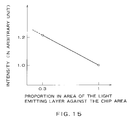
- Fig. 15 is a graph showing a relationship between the proportion in area of the light emitting layer against the chip area and the intensity of an externally emitted light for such an InGaAlP-based LED having a transparent substrate as exemplified in Fig. 14. That is to say, this drawing gives the data of the InGaAlP-based LED formed by GaP substrates with a chip size of 300 ⁇ m ⁇ 300 ⁇ m and an upper-side electrode diameter of 120 ⁇ m.
- the intensity of the light emitted increases, so that at a ratio of the area of 0.3, the light emitting intensity becomes about 1.2 times that at a ratio of 1.0.
- the light emitting efficiency can be improved while suppressing a decrease in the light take-out efficiency.
- Figs. 16A-17C are flow diagrams showing important steps in the preparation process of the semiconductor light emitting element according to this embodiment.
- Epitaxial wafers to be directly bonded to each other had such a configuration as shown in Fig. 16A, i.e. on the GaAs substrate 12 were epitaxial layers 93 through 982 by the MOCVD method.
- the n-type GaAs substrate 12 has a diameter of two inches, a thickness of 250 ⁇ m, and a carrier concentration of about 1 ⁇ 10 18 /cm 3 by means of Si doping and is mirror-finished.
- An etching stop layer 93 is made of InAlP and has a thickness of 0.2 ⁇ m.
- a GaAs contact layer 94 has a thickness of 0.02 ⁇ m and a carrier concentration of 1 ⁇ 10 18 /cm 3 .
- An InGaAlP current-spread layer 95 is made of InGaAlP with an Al composition ratio of 0.3 and has a thickness of 1.5 ⁇ m, while the n-type cladding layer 14 is made of InGaAlP with an Al composition ratio of 0.6 and has a thickness of 0.6 ⁇ m.
- An active layer 15 is made of InGaAlP with an Al composition of 0.13 and has a thickness of 0.4 ⁇ m.
- a p-type cladding layer 16 is made of InGaAlP with an Al composition ratio of 0.6 and has a thickness of 0.6 ⁇ m.
- An InGaP bonding layer 97 has a thickness of 0.1 ⁇ m, a GaAs cover layer 981 has a thickness of 0.1 ⁇ m, and an InAlP cover layer 982 has a thickness of 0.15 ⁇ m.
- this epitaxial wafer was washed with an interfacial active agent and immersed in a mixture solution consisting in volume of one part of ammonia and 15 parts of hydrogen peroxide solution to etch the lower side of the GaAs substrate 12 in order to remove the epitaxial reaction product attached on the back side of the epitaxial wafer.
- the top side of the epitaxial wafer (upper side in this drawing) was not etched because it was covered with the InAlP cover layer 98.
- the epitaxial wafer was washed again with an interfacial active agent and then with a phosphoric acid to remove the InAlP cover layer 982 on the top side.
- the GaAs cover layer 981 was removed using a mixture solution consisting in volume of eight parts of a sulfuric acid, one part of a hydrogen peroxide solution, and one part of water. This mixture solution was used to selectively etch the GaAs cover layer, so that after etching, the InGaP bonding layer was exposed on the top side of the epitaxial wafer.
- the epitaxial wafer with its top-side cover layer removed was directly bonded to the GaP wafer 11, to obtain an bonded couple shown in Fig. 16B.
- the process of this direct bonding is detailed as follows.
- such a p-type mirror-finished wafer was used that has a diameter of two inches and a thickness of 250 ⁇ m.
- a high-concentration layer may sometimes be epitaxial-grown on the surface of the GaP wafer.
- the GaP wafer was washed with an interfacial active agent and immersed in a dilute hydrofluoric acid to remove a natural oxide film on the surface, washed with water, and then dried with a spinner.
- the wafer as finished of the pretreatment was placed with its top side facing upward, on which was placed the GaP wafer 11 with its mirror face facing downward, so that they were bonded to each other at room temperature.
- the GaP wafer 11 is transparent, so that the bonding state can be observed by visual inspection. Since the epitaxial wafer was warped in convex when they were superposed one on top of the other, the wafers were tightly bonded first from their middle. Only left as is, the tightly bonded portion naturally spread, thus permitting the whole surface except the chamfered portions at the wafer periphery to be bonded tightly.
- the wafers tightly bonded at room temperature were arranged vertically on a quartz-made board and then placed in a diffusion furnace for the heat treatment.
- the heat treatment was conducted at 800°C in an argon atmosphere containing 10% of hydrogen for one hour.
- the GaAs substrate 12 was removed of the epitaxial wafer.
- the bonding couple was immersed in a mixture solution consisting of ammonia and a hydrogen peroxide solution to selectively etch GaAs. This etching stopped at the InAlP etching stop layer. Then, it was etched with a phosphoric acid at 70°C to selectively remove the InAlP etching stop layer 93, thereby obtaining such a laminate as shown in Fig. 16C.
- a electrode 19B made of a gold (Au)/Zn alloy and gold (Au)
- an electrode 19A made of a gold (Au)/Ge alloy and gold (Au).
- the PEP photo-engraving process
- the upper-side electrode 19A was processed at a 300- ⁇ m pitch into a circle with a diameter of 200 ⁇ m, thus obtaining such a structure as shown in Fig. 17A.
- the GaAs epitaxial layer 94 was etched with a mixture solution consisting of ammonia and a hydrogen peroxide solution, while the InGaAlP-based epitaxial layers 94 through 16 and the InGaP-based epitaxial layer 97 were etched with a IIBr-Br solution.
- the electrode 19A was patterned again into a circle with a diameter of 120 ⁇ m, to cleave the wafer at a dash-and-dot line C into sections of 300- ⁇ m ⁇ , thereby obtaining an LED chip having such a configuration as shown in Fig. 14A.
- Fig. 18 is a process cross-sectional view showing important steps of performing the this embodiment.
- such an epitaxial wafer was formed that has the laminate 10 formed as the light emitting layer on the GaAs substrate 12.
- This epitaxial wafer was subjected to blade dicing both horizontally and vertically at e.g. a 300- ⁇ m pitch, thereby providing a trench G with a width of 100 ⁇ m and a depth of 20 ⁇ m.
- the GaAs substrate 11 was bonded.
- the GaAs substrate 12 was removed, so that the bonded couple was turned upside down, to thus form thereon the electrodes 19A and 19B.
- the trench G was formed on the epitaxial top side when the wafers were bonded to each other and the bonding portion was divided into small-area sections, so that the stress can be relaxed, thus advantageously reducing the warp and the destruction.
- the wafers when the wafers are bonded to each other, air may be captured between these two wafers, thus creating non-bonded portion.
- the trench G such as given in this example permits the captured air to escape out of the wafers, thus advantageously reducing the possibility of non-bonded portion being created.
- the trench G may be formed by patterning the wafer by the PEP.
- Fig. 19 is a schematic diagram showing a variant example of the semiconductor device according to thus embodiment. That is to say, in this variant example, the laminate 10 as the light emitting layer was reduced in area to almost the same as the upper-side electrode 19A.
- the top side of the laminate 10 as the light emitting layer is wholly covered with the electrode 19A, so that a light emitted upward from the light emitting layer is reflected at the electrode 19A and enters the transparent substrate 11 to be taken out either from the side face of the substrate 11 or from the upper face S of the substrate 11 not covered by the electrode 19A.
- the light emitting element according to this variant example differs from the example of Fig. 14A or the conventional example of Fig. 14B in a respect that little of the light taken out from the upper face of the LED passes through the light emitting layer 15. That is to say, in this variant example, the active layer 15 acts as a comparatively small light source, so that most of the light emitted from this light source passes through the substrate 11 and is reflected at the lower-side electrode 19B, to be taken out from the upper face S.
- the wavelength of the light emitted from the LED depends on a band gap of the active layer 15.
- the cladding layers 14 and 16 are designed to have a larger band gap than the active layer in order to enclose the carriers, thus failing to absorb the light from the active layer 15.
- the active layer 15 itself, however, absorbs the light it emitted itself.
- such a GaAs contact layer necessary for electrical connection that has a small band gap also absorbs an emitted light. Therefore, it is preferable because of less absorption to take out the light without passing it through the active layer or contact layer including such a layer that absorbs light. In this respect, this variant example shown in Fig. 18 is advantageous.
- the electrode 19A shown in Fig. 17A may be patterned first time with a size shown in Fig. 17C and then used as a mask to etch the light emitting layer.
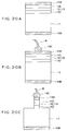
- Fig. 20 is a process cross-sectional view showing important steps in a preparation process of a semiconductor light emitting element shown in Fig. 19.
- the wafers are divided, without being patterned, into chips with both the upper-side and lower-side electrodes 19A and 19B of the LED as attached on the whole surface.
- the laminate 10 can be electrified via the wire W during etching, thus emitting a light. That is to say, it is also possible to permit the light emitting element to emit a light while monitoring its power during etching, thus stopping the etching immediately after an optimal light-emission intensity is obtained.
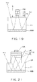
- Fig. 21 is a concept diagram showing a configuration of the semiconductor light emitting element according to this example. That is to say, the light emitting element of this example is provided with a step ST on a side face of its transparent substrate 11, the upper part of which is made small to match the size of the laminate 10 given as the light emitting layer.
- This structure can be obtained by bonding the GaP wafer 11 to the GaAs substrate (not shown) and selectively etching it off and then, in such a state as shown in Fig. 16C or 16A, providing a trench by blade dicing or etching in the transparent substrate 11 from the light emitting layer side beyond the light emitting layer up to the upper part of that substrate 11.
- the transparent substrate 11 is provided with the step, thus further improving the light-take-out efficiency.
- the transparent substrate 11 has its upper side smaller than the lower side by one step, it may should be made further smaller by two steps or more in order to obtain an even higher light-take-out efficiency.
- the materials of those semiconductor device are not limited to GaAs and Gap but may be any other various compound semiconductors applied to the present invention, to obtain almost the same effects as mentioned above.
- the laminate structure of the semiconductor light emitting element may be provided, in addition, with various components such as a contact layer and a current-spread layer, to have the same effects.
- various components such as a contact layer and a current-spread layer, to have the same effects.
- an MQW (multiple-quantum well) structure may be employed or as the cladding layer, an MQB (multiple-quantum barrier) may be employed in application.
- the present invention can be applied not only to LEDs but also to semiconductor lasers or other various semiconductor devices.
- the present invention has the following effects.
- the present invention will eliminate obstructions against the direction bonding such as deterioration of the cleanness of epitaxial wafer surfaces, their warp, and a difference in thermal expansion between the epitaxial-grown layer and the substrate, thus providing a bonding type semiconductor substrate which is tightly bonded directly and wholly to the epitaxial wafer.
- the present invention permits an epitaxial-grown layer contributing to light emission by such a light emitting element as an LED to be directly and in a stable manner bonded to a substrate not absorbing thus emitted light, thus providing a high-brightness semiconductor light emitting element.
- the present invention enables the production at a higher yield of both the bonding type semiconductor substrate and the semiconductor light emitting element which have the above-mentioned effects.
- the present invention by bonding "the top side” and “the back side” of wafers sliced off ingots taking into account the crystal anisotropy, it is possible to reduce dangling bonds and crystal defects at the interface, thus significantly lowering the interface resistance.
- the present invention makes it possible to partially holding and pressurizing the two wafers when they are bonded to each other, thus performing the bonding process with a high yield.
- the light emitting layer by making the light emitting layer smaller in area than the transparent substrate, the light-emission efficiency can be improved without lowering the LED's take-out efficiency, thus resulting in high-brightness LEDs being obtained.
Landscapes
- Led Devices (AREA)
- Semiconductor Lasers (AREA)
Abstract
Description
Claims (37)
- A bonding type semiconductor substrate comprising:a first semiconductor substrate;a first epitaxial growth layer formed on said first semiconductor substrate, anda second semiconductor substrate whose at least one surface has been mirror-finished and which is integrally joined to said first epitaxial growth layer via the mirror-finished surface,a thermal expansion coefficient of said first epitaxial growth layer being close to the thermal expansion coefficient of said second semiconductor substrate.
- The bonding type semiconductor substrate according to claim 1 further comprising a second epitaxial growth layer grown on said mirror-finished surface of said second semiconductor substrate, ;said second semiconductor substrate being integrally joined to said first epitaxial growth layer via said second epitaxial growth layer.
- The bonding type semiconductor substrate according to claim 2 wherein:said first semiconductor substrate is formed from GaAs,said first epitaxial growth layer includes a compound semiconductor layer represented by the composition formula Inx(Ga1-yAly)1-xP (0.45<x<0.50, 0≤y≤1),said second semiconductor substrate is formed from GaP, andsaid second epitaxial growth layer includes GaP as a main component.
- A semiconductor light emitting element comprising:a first epitaxial growth layer formed from mixed crystals of a compound semiconductor on a first semiconductor substrate, said first epitaxial growth layer including a first cladding layer formed by selecting a composition ratio of the mixed crystals so as to match a lattice constant of said first semiconductor substrate, an active layer formed on said first cladding layer, and a second cladding layer formed on said active layer; said first semiconductor substrate being removed from the first epitaxial growth layer;a second semiconductor substrate whose a main surface is mirror-finished and which is directly bonded to said first epitaxial growth layer via the mirror-finished surface or a second epitaxial growth layer grown on the mirror-finished surface; andelectrodes which are formed on the front side of said first cladding layer and on the back side of said second semiconductor substrate and which supplies an electric current to said active layer,said first semiconductor substrate being formed from GaAs,said first epitaxial growth layer being represented by the composition formula Inx(Ga1-yAly)1-xP,a composition ratio of said first cladding layer in said composition formula being 0.45<x<0.50 and 0≤y≤1,said second semiconductor substrate being formed from GaP, andsaid second epitaxial growth layer containing GaP as a main component.
- The semiconductor light emitting element according to claim 4, wherein a thermal expansion coefficient of said first epitaxial growth layer is close to the thermal expansion coefficient of said second semiconductor substrate.
- A bonding type semiconductor substrate comprising:a first semiconductor substrate whose at least one surface is mirror-finished; anda second semiconductor substrate whose at least one surface is mirror-finished and which is integrally joined to said mirror-finished surface of said first semiconductor substrate via the mirror-finished surface,a crystal orientation of the bonded surface of said second semiconductor substrate being much the same as a crystal orientation of the back surface which is opposite to the bonded surface of the first semiconductor substrate.
- A bonding type semiconductor substrate comprising:an epitaxial growth layer formed on a first semiconductor substrate; anda second semiconductor substrate whose at least one surface is mirror-finished and which is integrally joined to said epitaxial growth layer via the mirror-finished surface,a crystal orientation of the bonded surface of said second semiconductor substrate being much the same as a crystal orientation of the back surface which is opposite to the bonded surface of the first semiconductor substrate.
- A bonding type semiconductor substrate comprising:a first epitaxial growth layer formed on a first semiconductor substrate; anda second semiconductor substrate on which a second epitaxial growth layer is grown at least one surface and which is integrally joined to said first epitaxial growth layer via said second epitaxial growth layer,a crystal orientation of the bonded surface of said second semiconductor substrate being much the same as a crystal orientation of the back surface which is opposite to the bonded surface of the first semiconductor substrate.
- A bonding type semiconductor substrate comprising:a first epitaxial growth layer formed on a first semiconductor substrate; anda second semiconductor substrate whose at least one surface is mirror-finished and which is integrally joined to said first epitaxial growth layer via the mirror-finished surface or a second epitaxial growth layer grown on the mirror-finished surface,both of said first semiconductor substrate and said second semiconductor substrate being made from compounds,a surface where a (111) A plane preferentially appears in the main surface of the second semiconductor substrate being bonded to a surface where a (111) B plane preferentially appears in the main surface of said first semiconductor substrate, or a surface where a (111) B plane preferentially appears in the main surface of the second semiconductor substrate being bonded to a surface where a (111) A plane preferentially appears in the main surface of said first semiconductor substrate.
- The bonding type semiconductor substrate according to claim 8, wherein said first semiconductor substrate is formed from GaAs,said first epitaxial growth layer includes a compound semiconductor layer represented by the formula Inx(Ga1-yAly)1-xP (0.45<x<0.50, 0≤y≤1),said second semiconductor substrate is formed from Gap, andsaid second epitaxial growth layer contains GaP as a main component.
- The bonding type semiconductor substrate according to claim 6, wherein said first semiconductor substrate and said second semiconductor substrate are bonded and integrated so that normal-mesa directions on the joined surfaces may cross each other at right angles.
- The bonding type semiconductor substrate according to claim 6, wherein said first semiconductor substrate has a surface inclining in a direction of from a (100) plane toward a (111) group III gallium plane direction at a first inclining angle, andsaid second semiconductor substrate has a surface inclining in a direction of from (100) plane toward a (111) group V phosphorus plane direction at a second inclining angle.
- The bonding type semiconductor substrate according to claim 12, wherein said first inclining angle is much the same as said second inclining angle.
- A semiconductor light emitting element comprising a remaining part of a bonding type semiconductor substrate,said bonding type semiconductor substrate having:a first epitaxial growth layer formed on a first semiconductor substrate; anda second semiconductor substrate whose at least one surface is mirror-finished and which is integrally joined to said first epitaxial growth layer via the mirror-finished surface or a second epitaxial growth layer grown on the mirror-finished surface,both of said first semiconductor substrate and said second semiconductor substrate being made from compounds,a surface where a (111) A plane preferentially appears in the main surface of the second semiconductor substrate being bonded to a surface where a (111) B plane preferentially appears in the main surface of said first semiconductor substrate, or a surface where a (111) B plane preferentially appears in the main surface of the second semiconductor substrate being bonded to a surface where a (111) A plane preferentially appears in the main surface of said first semiconductor substratesaid remaining part being obtained by removing at least part of said first semiconductor substrate from said bonding type semiconductor substrate.
- A semiconductor light emitting element comprising a light emitting layer and a substrate having a transparency to emission, whereinan area of said light emitting layer on said substrate is smaller than an area of said substrate.
- The semiconductor light emitting element according to claim 15, wherein said substrate has a step on the side thereof so that an area of a main surface on the side of said emitting layer of the main surfaces may be smaller than an area of the main surface on a reverse side.
- A process for preparing a bonding type semiconductor substrate comprising:a first step of forming a first epitaxial growth layer by epitaxially growing semiconductor crystals on a first semiconductor substrate,a second step of removing contaminants and dust particles from the surface of said first epitaxial growth layer, anda third step of integrally joining, to said first epitaxial growth layer from which the contaminants and the dust particles are removed in the second step, a second semiconductor substrate whose at least one surface is mirror-finished, by placing the substrate on the first epitaxial growth layer so that the substrate may come into contact with the first epitaxial growth layer via the mirror-finished surface or a second epitaxial growth layer grown on the mirror-finished surface.
- A process for preparing a bonding type semiconductor substrate comprising:a first step of forming an epitaxial growth layer by epitaxially growing semiconductor crystals on a first semiconductor substrate by selecting a composition ratio so as to match a lattice constant of the first semiconductor substrate,a second step of removing contaminants and dust particles from the surface of said epitaxial growth layer, anda third step of integrally joining a second semiconductor substrate, whose at least one surface is mirror-finished, to said epitaxial growth layer by placing the substrate on the epitaxial growth layer so that the substrate may come into contact with the epitaxial growth layer via the mirror-finished surface.
- The process for preparing a bonding type semiconductor substrate according to claim 18 further comprising a forth step of subjecting the resultant laminate to a heat treatment after at least part of the surface of said first semiconductor substrate has been removed therefrom.
- The process for preparing the bonding type semiconductor substrate according to claim 18, wherein said first step comprises a step of forming a cover layer on said epitaxial growth layer andsaid second step is a step of removing said cover layer by etching.
- The process for preparing the bonding type semiconductor substrate according to claim 18, wherein said second step is a step of removing a surface part of said epitaxial growth layer.
- A process for preparing a semiconductor light emitting element comprising:a step of forming a first epitaxial growth layer comprising a laminate where a first cladding layer, an active layer, and a second cladding layer are deposited in turn on a first semiconductor substrate by growing mixed crystals of a compound semiconductor,a step of forming a cover layer on said first epitaxial growth layer,a step of exposing a surface of said first epitaxial growth layer by removing said cover layer,a step of integrally joining a second semiconductor substrate having a mirror-finished main surface to said first epitaxial growth layer having the exposed surface by placing the substrate on said first epitaxial growth layer so that said main surface of the substrate may come into contact with said first epitaxial growth layer,a step of subjecting the laminate to a heat treatment at a temperature below a temperature at which the bonding surface is broken owing to a difference between thermal expansion coefficients of said first semiconductor substrate and said second semiconductor substrate,a step of exposing said first epitaxial growth layer by removing said first semiconductor substrate, anda step of forming electrodes on the front side of said first epitaxial growth layer and on the back side of said second semiconductor substrate.
- The process for preparing the semiconductor light emitting element according to claim 22, wherein said first cladding layer is formed by selecting a composition ratio of said mixed crystals so that a lattice constant of the cladding layer may match a lattice constant of said first semiconductor substrate,said first semiconductor substrate is formed from GaAs,said first laminate is a compound semiconductor layer represented by the formula Inx(Ga1-yAly)1-xP,a composition ratio of said first cladding layer in said formula is 0.45<x<0.50 and 0≤y≤1, andsaid second semiconductor substrate is formed from GaP.
- A process for preparing a semiconductor light emitting element comprising:a step of forming an epitaxial growth layer comprising a laminate where a first cladding layer, an active layer, and a second cladding layer are deposited in turn on a first semiconductor substrate by epitaxially growing mixed crystals of a compound semiconductor,a step of forming a cover layer on said second cladding layer,a step of exposing the surface of said second cladding layer by removing said cover layer,a step of integrally bonding a second semiconductor substrate having a mirror-finished main surface to said second cladding layer having the exposed surface by placing the substrate on said second cladding layer so that said main surface of the substrate may come into contact with said second cladding layer,a step of carrying out a heat treatment after at least a surface part of said first semiconductor substrate has been removed by etching,a step of exposing said first cladding layer by etching, anda step of forming electrodes on the front side of said first cladding layer and on the back side of said second semiconductor substrate.
- The process for preparing the semiconductor light emitting element according to claim 24, wherein said epitaxial growth layer is formed between said first semiconductor substrate and said laminate and contains a protective film which functions as an etching stopper in the step of removing said first semiconductor substrate.
- A process for preparing a semiconductor light emitting element comprising the steps of:making a light emitting body including a light emitting layer; andintegrally bonding a first and a second semiconductor substrates and said light emitting body by a heat treatment at a high temperature after sandwiching said light emitting body by said first and second semiconductor substrates.
- The process for preparing a semiconductor light emitting element according to claim 26, wherein said integrally bonding step is conducted so that the bonding of said light emitting body and said first semiconductor substrate and the bonding of said light emitting body and said second semiconductor substrate are performed at once by said heat treatment.
- A process for preparing a semiconductor light emitting element comprising the steps of:epitaxially growing a light emitting body including a light emitting layer on a growth substrate;placing a first semiconductor substrate on a upper surface of said light emitting body in a close contact at a first temperature;removing said growth substrate so that the lower surface of said light emitting body is exposed;placing a second semiconductor substrate on said lower surface of said light emitting body in a close contact at a second temperature; andintegrally bonding said light emitting body and said first and second semiconductor substrates by annealing at a third temperature higher than said first and second temperature.
- The process for preparing a semiconductor light emitting element according to claim 28, wherein said third temperature is higher than 500 °C and lower than 1200 °C.
- A process for preparing a bonding type semiconductor substrate by joining a first and a second semiconductor substrates to each other, wherein a surface where a (111) A plane preferentially appears in the main surface of said second semiconductor substrate made of a compound semiconductor is joined to a surface where a (111) B plane preferentially appears in the main surface of said first semiconductor substrate made of a compound semiconductor, or a surface where a (111) B plane preferentially appears in the main surface of said second semiconductor substrate made of a compound semiconductor is joined to a surface where a (111) A plane preferentially appears in the main surface of said first semiconductor substrate made of a compound semiconductor.
- A process for preparing a bonding type semiconductor substrate by joining a first and a second semiconductor substrates obtained by slicing off a single crystal ingot made of a compound semiconductor, whereina main surface part far from a seed crystal of said single crystal ingot in the main surface of the second semiconductor substrate is joined to a main surface part near to said seed crystal of said single crystal ingot in the main surface of said first semiconductor substrate.
- A process for preparing a bonding type semiconductor substrate by joining a first semiconductor substrate obtained by slicing off a first single crystal ingot made of a compound semiconductor and a second semiconductor substrates obtained by slicing off a second single crystal ingot made of a compound semiconductor, whereina main surface part far from a seed crystal of said second single crystal ingot in the main surface of the second semiconductor substrate is joined to a main surface part near to a seed crystal of said first single crystal ingot in the main surface of said first semiconductor substrate.
- A process for preparing a bonding type semiconductor substrate by joining two semiconductor substrates to each other, whereinsaid two semiconductor substrates are joined by heating them, while only a part of said two laminated semiconductor substrates are pressed and the other parts of said two semiconductor substrate are not pressed.
- The process for preparing the bonding type semiconductor substrate according to claim 33, wherein only a central part of said two laminated semiconductor substrates are pressed.
- The process for preparing the semiconductor light emitting element according to claim 22 further comprising the step of partially removing said active layer to thereby make an area of said active layer on said second semiconductor substrate smaller than an area of said second semiconductor substrate.
- The process for preparing the semiconductor light emitting element according to claim 17, wherein a groove is formed on the surface to be joined of at least one of said first semiconductor substrate and said second semiconductor substrate prior to the joining.
- A semiconductor light emitting element comprising:a light emitting body including a light emitting layer;a first semiconductor substrate integrally joined to one major face of said light emitting body; anda second semiconductor substrate integrally joined to another major face of said light emitting body.
Applications Claiming Priority (6)
| Application Number | Priority Date | Filing Date | Title |
|---|---|---|---|
| JP16298599 | 1999-06-09 | ||
| JP16298599 | 1999-06-09 | ||
| JP17413899A JP2001007389A (en) | 1999-06-21 | 1999-06-21 | Method for manufacturing semiconductor light emitting device |
| JP17413899 | 1999-06-21 | ||
| JP2000089754A JP3977572B2 (en) | 1999-06-09 | 2000-03-28 | Adhesive semiconductor substrate, semiconductor light-emitting device, and method for manufacturing the same |
| JP2000089754 | 2000-03-28 |
Publications (3)
| Publication Number | Publication Date |
|---|---|
| EP1065734A2 true EP1065734A2 (en) | 2001-01-03 |
| EP1065734A3 EP1065734A3 (en) | 2001-12-19 |
| EP1065734B1 EP1065734B1 (en) | 2009-05-13 |
Family
ID=27322093
Family Applications (1)
| Application Number | Title | Priority Date | Filing Date |
|---|---|---|---|
| EP00304862A Expired - Lifetime EP1065734B1 (en) | 1999-06-09 | 2000-06-08 | Bonding type semiconductor substrate, semiconductor light emitting element, and preparation process thereof. |
Country Status (4)
| Country | Link |
|---|---|
| US (6) | US6465809B1 (en) |
| EP (1) | EP1065734B1 (en) |
| DE (1) | DE60042187D1 (en) |
| TW (1) | TW502458B (en) |
Cited By (4)
| Publication number | Priority date | Publication date | Assignee | Title |
|---|---|---|---|---|
| EP1202355A2 (en) * | 2000-10-31 | 2002-05-02 | Kabushiki Kaisha Toshiba | Semiconductor light-emitting device and method of manufacturing the same |
| EP1727215A2 (en) | 2005-05-23 | 2006-11-29 | Samsung Electro-Mechanics Co., Ltd. | Vertical structure semiconductor light emitting device and method for manufacturing the same |
| CN101218686B (en) * | 2005-07-06 | 2012-02-29 | 昭和电工株式会社 | Compound semiconductor light emitting diode and manufacturing method thereof |
| US10490688B2 (en) | 2011-10-11 | 2019-11-26 | Soitec | Multi junctions in a semiconductor device formed by different deposition techniques |
Families Citing this family (75)
| Publication number | Priority date | Publication date | Assignee | Title |
|---|---|---|---|---|
| DE60042187D1 (en) * | 1999-06-09 | 2009-06-25 | Toshiba Kawasaki Kk | Bond-type semiconductor substrate, semiconductor light-emitting device, and manufacturing method |
| JP3910817B2 (en) * | 2000-12-19 | 2007-04-25 | ユーディナデバイス株式会社 | Semiconductor photo detector |
| US7233028B2 (en) * | 2001-02-23 | 2007-06-19 | Nitronex Corporation | Gallium nitride material devices and methods of forming the same |
| TWI294699B (en) * | 2006-01-27 | 2008-03-11 | Epistar Corp | Light emitting device and method of forming the same |
| TW541732B (en) * | 2002-08-28 | 2003-07-11 | Arima Optoelectronics Corp | Manufacturing method of LED having transparent substrate |
| JP4116387B2 (en) * | 2002-09-30 | 2008-07-09 | 株式会社東芝 | Semiconductor light emitting device |
| US7041529B2 (en) * | 2002-10-23 | 2006-05-09 | Shin-Etsu Handotai Co., Ltd. | Light-emitting device and method of fabricating the same |
| US6786390B2 (en) * | 2003-02-04 | 2004-09-07 | United Epitaxy Company Ltd. | LED stack manufacturing method and its structure thereof |
| WO2004100279A2 (en) | 2003-04-30 | 2004-11-18 | Cree, Inc. | High-power solid state light emitter package |
| JP3737494B2 (en) * | 2003-06-10 | 2006-01-18 | 株式会社東芝 | Semiconductor light emitting device, method for manufacturing the same, and semiconductor light emitting device |
| EP1649514B1 (en) * | 2003-07-30 | 2014-01-01 | Panasonic Corporation | Semiconductor light emitting device, light emitting module, and lighting apparatus |
| KR101014720B1 (en) * | 2004-01-19 | 2011-02-16 | 엘지전자 주식회사 | Semiconductor laser diode manufacturing method |
| US7332365B2 (en) * | 2004-05-18 | 2008-02-19 | Cree, Inc. | Method for fabricating group-III nitride devices and devices fabricated using method |
| US7791061B2 (en) | 2004-05-18 | 2010-09-07 | Cree, Inc. | External extraction light emitting diode based upon crystallographic faceted surfaces |
| US7534633B2 (en) * | 2004-07-02 | 2009-05-19 | Cree, Inc. | LED with substrate modifications for enhanced light extraction and method of making same |
| JP2006066449A (en) * | 2004-08-24 | 2006-03-09 | Toshiba Corp | Semiconductor light emitting device |
| JP4250576B2 (en) * | 2004-08-24 | 2009-04-08 | 株式会社東芝 | Semiconductor light emitting device |
| JP2006080314A (en) * | 2004-09-09 | 2006-03-23 | Canon Inc | Manufacturing method of bonded substrate |
| JP4518886B2 (en) * | 2004-09-09 | 2010-08-04 | シャープ株式会社 | Manufacturing method of semiconductor device |
| US7259402B2 (en) * | 2004-09-22 | 2007-08-21 | Cree, Inc. | High efficiency group III nitride-silicon carbide light emitting diode |
| US8174037B2 (en) * | 2004-09-22 | 2012-05-08 | Cree, Inc. | High efficiency group III nitride LED with lenticular surface |
| US8513686B2 (en) | 2004-09-22 | 2013-08-20 | Cree, Inc. | High output small area group III nitride LEDs |
| US7737459B2 (en) * | 2004-09-22 | 2010-06-15 | Cree, Inc. | High output group III nitride light emitting diodes |
| JP2006156950A (en) * | 2004-10-29 | 2006-06-15 | Sharp Corp | Manufacturing method of semiconductor light emitting device |
| US8288942B2 (en) | 2004-12-28 | 2012-10-16 | Cree, Inc. | High efficacy white LED |
| KR100763402B1 (en) * | 2005-01-07 | 2007-10-05 | 엘지전자 주식회사 | Lighting device |
| US7932111B2 (en) | 2005-02-23 | 2011-04-26 | Cree, Inc. | Substrate removal process for high light extraction LEDs |
| KR100638732B1 (en) * | 2005-04-15 | 2006-10-30 | 삼성전기주식회사 | Manufacturing method of vertical structure nitride semiconductor light emitting device |
| TWI253770B (en) * | 2005-07-11 | 2006-04-21 | Univ Nat Central | Light emitting diode and manufacturing method thereof |
| US8674375B2 (en) * | 2005-07-21 | 2014-03-18 | Cree, Inc. | Roughened high refractive index layer/LED for high light extraction |
| KR100738079B1 (en) * | 2005-10-19 | 2007-07-12 | 삼성전자주식회사 | Manufacturing method of nitride semiconductor laser diode |
| US20070181927A1 (en) * | 2006-02-03 | 2007-08-09 | Yedinak Joseph A | Charge balance insulated gate bipolar transistor |
| TWI303115B (en) * | 2006-04-13 | 2008-11-11 | Epistar Corp | Semiconductor light emitting device |
| US8581274B2 (en) * | 2006-05-01 | 2013-11-12 | Mitsubishi Chemical Corporation | Integrated semiconductor light-emitting device and its manufacturing method |
| JP2009538536A (en) | 2006-05-26 | 2009-11-05 | クリー エル イー ディー ライティング ソリューションズ インコーポレイテッド | Solid state light emitting device and method of manufacturing the same |
| JP2009539227A (en) | 2006-05-31 | 2009-11-12 | クリー エル イー ディー ライティング ソリューションズ インコーポレイテッド | Lighting device and lighting method |
| JP5003033B2 (en) * | 2006-06-30 | 2012-08-15 | 住友電気工業株式会社 | GaN thin film bonded substrate and manufacturing method thereof, and GaN-based semiconductor device and manufacturing method thereof |
| US8310143B2 (en) * | 2006-08-23 | 2012-11-13 | Cree, Inc. | Lighting device and lighting method |
| US9310026B2 (en) | 2006-12-04 | 2016-04-12 | Cree, Inc. | Lighting assembly and lighting method |
| WO2008070604A1 (en) * | 2006-12-04 | 2008-06-12 | Cree Led Lighting Solutions, Inc. | Lighting device and lighting method |
| TWI331411B (en) * | 2006-12-29 | 2010-10-01 | Epistar Corp | High efficiency light-emitting diode and method for manufacturing the same |
| JP4973888B2 (en) * | 2007-01-26 | 2012-07-11 | 信越半導体株式会社 | Light emitting device and manufacturing method thereof |
| US8021904B2 (en) * | 2007-02-01 | 2011-09-20 | Cree, Inc. | Ohmic contacts to nitrogen polarity GaN |
| EP2171502B1 (en) | 2007-07-17 | 2016-09-14 | Cree, Inc. | Optical elements with internal optical features and methods of fabricating same |
| US8617997B2 (en) * | 2007-08-21 | 2013-12-31 | Cree, Inc. | Selective wet etching of gold-tin based solder |
| US11114594B2 (en) | 2007-08-24 | 2021-09-07 | Creeled, Inc. | Light emitting device packages using light scattering particles of different size |
| US8368100B2 (en) | 2007-11-14 | 2013-02-05 | Cree, Inc. | Semiconductor light emitting diodes having reflective structures and methods of fabricating same |
| US9634191B2 (en) | 2007-11-14 | 2017-04-25 | Cree, Inc. | Wire bond free wafer level LED |
| US9431589B2 (en) | 2007-12-14 | 2016-08-30 | Cree, Inc. | Textured encapsulant surface in LED packages |
| JP5277646B2 (en) * | 2008-01-25 | 2013-08-28 | 信越半導体株式会社 | Method for manufacturing compound semiconductor substrate |
| JP5315070B2 (en) * | 2008-02-07 | 2013-10-16 | 昭和電工株式会社 | Compound semiconductor light emitting diode |
| US8299480B2 (en) * | 2008-03-10 | 2012-10-30 | Kabushiki Kaisha Toshiba | Semiconductor light emitting device and method for manufacturing same, and epitaxial wafer |
| DE102008021620A1 (en) * | 2008-04-30 | 2009-11-05 | Osram Opto Semiconductors Gmbh | A radiation-emitting thin-film semiconductor chip and method for producing a radiation-emitting thin-film semiconductor chip |
| EP2302705B1 (en) * | 2008-06-02 | 2018-03-14 | LG Innotek Co., Ltd. | Supporting substrate for fabrication of semiconductor light emitting device and semiconductor light emitting device using the same |
| US8384115B2 (en) * | 2008-08-01 | 2013-02-26 | Cree, Inc. | Bond pad design for enhancing light extraction from LED chips |
| JP2010045156A (en) * | 2008-08-12 | 2010-02-25 | Toshiba Corp | Method of producing semiconductor device |
| JP2010186829A (en) * | 2009-02-10 | 2010-08-26 | Toshiba Corp | Method for manufacturing light emitting element |
| JP2010219320A (en) * | 2009-03-17 | 2010-09-30 | Toshiba Corp | Method of manufacturing light-emitting element and light-emitting element |
| US8741715B2 (en) * | 2009-04-29 | 2014-06-03 | Cree, Inc. | Gate electrodes for millimeter-wave operation and methods of fabrication |
| JP2011198962A (en) * | 2010-03-18 | 2011-10-06 | Toshiba Corp | Method for manufacturing semiconductor light emitting element |
| US8329482B2 (en) | 2010-04-30 | 2012-12-11 | Cree, Inc. | White-emitting LED chips and method for making same |
| JP5684501B2 (en) * | 2010-07-06 | 2015-03-11 | 昭和電工株式会社 | Epitaxial wafer for light emitting diode |
| US9070851B2 (en) | 2010-09-24 | 2015-06-30 | Seoul Semiconductor Co., Ltd. | Wafer-level light emitting diode package and method of fabricating the same |
| CN103650171B (en) * | 2011-07-15 | 2018-09-18 | 亮锐控股有限公司 | Semiconductor device is attached to the method for supporting substrate |
| US8896008B2 (en) | 2013-04-23 | 2014-11-25 | Cree, Inc. | Light emitting diodes having group III nitride surface features defined by a mask and crystal planes |
| US9252324B2 (en) * | 2013-05-30 | 2016-02-02 | Globalfoundries Inc | Heterojunction light emitting diode |
| TWM468013U (en) * | 2013-07-18 | 2013-12-11 | 菘鐿科技有限公司 | Electronic industry process shared removable and replaceable wire hot plate |
| US9508894B2 (en) | 2013-07-29 | 2016-11-29 | Epistar Corporation | Method of selectively transferring semiconductor device |
| US9985190B2 (en) * | 2016-05-18 | 2018-05-29 | eLux Inc. | Formation and structure of post enhanced diodes for orientation control |
| USD826871S1 (en) | 2014-12-11 | 2018-08-28 | Cree, Inc. | Light emitting diode device |
| EP3182459A1 (en) * | 2015-12-15 | 2017-06-21 | IMEC vzw | Method of producing a pre-patterned structure for growing vertical nanostructures |
| CN205944139U (en) | 2016-03-30 | 2017-02-08 | 首尔伟傲世有限公司 | Ultraviolet ray light -emitting diode spare and contain this emitting diode module |
| DE102019114328B4 (en) * | 2018-05-31 | 2022-03-03 | Rohm Co. Ltd | SEMICONDUCTOR SUBSTRATE STRUCTURE AND POWER SEMICONDUCTOR DEVICE |
| US12426410B2 (en) | 2019-08-28 | 2025-09-23 | Tslc Corporation | Semiconductor components and semiconductor structures and methods of fabrication |
| CN112951713A (en) * | 2021-02-07 | 2021-06-11 | 长春长光圆辰微电子技术有限公司 | Processing method of small-size wafer |
Family Cites Families (62)
| Publication number | Priority date | Publication date | Assignee | Title |
|---|---|---|---|---|
| JPS58125638A (en) * | 1982-01-21 | 1983-07-26 | Toshiba Corp | Glass composition for coating semiconductor |
| JPH0770474B2 (en) * | 1985-02-08 | 1995-07-31 | 株式会社東芝 | Method for manufacturing compound semiconductor device |
| JPH0770472B2 (en) * | 1985-02-08 | 1995-07-31 | 株式会社東芝 | Method for manufacturing semiconductor substrate |
| JPS6227040A (en) | 1985-07-26 | 1987-02-05 | Sapporo Breweries Ltd | Method for adsorbing or including material to or into starch |
| JPS6276645A (en) * | 1985-09-30 | 1987-04-08 | Toshiba Corp | Structure of composite semiconductor crystal |
| JPS63226918A (en) * | 1987-03-16 | 1988-09-21 | Shin Etsu Handotai Co Ltd | Gallium phosphide arsenide mixed crystal epitaxial wafer |
| JP2788269B2 (en) * | 1988-02-08 | 1998-08-20 | 株式会社東芝 | Semiconductor device and manufacturing method thereof |
| US5332920A (en) * | 1988-02-08 | 1994-07-26 | Kabushiki Kaisha Toshiba | Dielectrically isolated high and low voltage substrate regions |
| US5512774A (en) * | 1988-02-08 | 1996-04-30 | Kabushiki Kaisha Toshiba | Dielectrically isolated substrate and semiconductor device using the same |
| US5049968A (en) * | 1988-02-08 | 1991-09-17 | Kabushiki Kaisha Toshiba | Dielectrically isolated substrate and semiconductor device using the same |
| JP2685819B2 (en) * | 1988-03-31 | 1997-12-03 | 株式会社東芝 | Dielectric isolated semiconductor substrate and manufacturing method thereof |
| EP0588449B1 (en) * | 1988-12-27 | 1997-08-06 | Canon Kabushiki Kaisha | Electric field light-emitting device |
| US5103271A (en) * | 1989-09-28 | 1992-04-07 | Kabushiki Kaisha Toshiba | Semiconductor light emitting device and method of fabricating the same |
| JPH03278542A (en) * | 1990-03-28 | 1991-12-10 | Hitachi Ltd | Semiconductor device |
| US5322920A (en) | 1990-07-25 | 1994-06-21 | Kanegafuchi Kagaku Kogyo Kabushiki Kaisha | Thermosetting esterimide oligomer and its production method |
| JPH04223380A (en) * | 1990-12-25 | 1992-08-13 | Stanley Electric Co Ltd | Led chip provided with substrate and manufacture thereof |
| KR930015139A (en) * | 1991-12-18 | 1993-07-23 | 이헌조 | Manufacturing method of light emitting diode capable of changing light intensity |
| JPH05235312A (en) * | 1992-02-19 | 1993-09-10 | Fujitsu Ltd | Semiconductor substrate and its manufacture |
| US5349211A (en) * | 1992-03-26 | 1994-09-20 | Nec Corporation | Semiconductor infrared emitting device with oblique side surface with respect to the cleavage |
| JP3192000B2 (en) * | 1992-08-25 | 2001-07-23 | キヤノン株式会社 | Semiconductor substrate and manufacturing method thereof |
| JP2905667B2 (en) * | 1992-12-17 | 1999-06-14 | シャープ株式会社 | Method for manufacturing II-VI compound semiconductor thin film and II-VI compound semiconductor device |
| JP3230638B2 (en) | 1993-02-10 | 2001-11-19 | シャープ株式会社 | Light emitting diode manufacturing method |
| US5459337A (en) * | 1993-02-19 | 1995-10-17 | Sony Corporation | Semiconductor display device with red, green and blue emission |
| JP3321882B2 (en) * | 1993-02-28 | 2002-09-09 | ソニー株式会社 | Substrate bonding method |
| JPH06326358A (en) | 1993-03-17 | 1994-11-25 | Ricoh Co Ltd | Semiconductor light emitting element |
| US5376580A (en) | 1993-03-19 | 1994-12-27 | Hewlett-Packard Company | Wafer bonding of light emitting diode layers |
| JPH06349692A (en) | 1993-06-08 | 1994-12-22 | Hitachi Ltd | Semiconductor device and manufacturing method thereof |
| US5461243A (en) * | 1993-10-29 | 1995-10-24 | International Business Machines Corporation | Substrate for tensilely strained semiconductor |
| JPH07161936A (en) | 1993-12-07 | 1995-06-23 | Toshiba Corp | Semiconductor memory device and manufacturing method thereof |
| TW289837B (en) | 1994-01-18 | 1996-11-01 | Hwelett Packard Co | |
| DE69503227T2 (en) | 1994-03-01 | 1999-03-25 | Bowthorpe Components Ltd., Crawley, West Sussex | THERMISTOR |
| JP2669368B2 (en) | 1994-03-16 | 1997-10-27 | 日本電気株式会社 | Method for manufacturing compound semiconductor laminated structure on Si substrate |
| JPH08148723A (en) | 1994-11-24 | 1996-06-07 | Matsushita Electric Ind Co Ltd | Optical printhead and manufacturing method thereof |
| US5821555A (en) * | 1995-03-27 | 1998-10-13 | Kabushiki Kaisha Toshiba | Semicoductor device having a hetero interface with a lowered barrier |
| JP3557011B2 (en) * | 1995-03-30 | 2004-08-25 | 株式会社東芝 | Semiconductor light emitting device and manufacturing method thereof |
| JP3734849B2 (en) * | 1995-05-08 | 2006-01-11 | 三菱電機株式会社 | Manufacturing method of semiconductor laser device |
| US5603779A (en) * | 1995-05-17 | 1997-02-18 | Harris Corporation | Bonded wafer and method of fabrication thereof |
| JP3197788B2 (en) * | 1995-05-18 | 2001-08-13 | 株式会社日立製作所 | Method for manufacturing semiconductor device |
| DE19629920B4 (en) | 1995-08-10 | 2006-02-02 | LumiLeds Lighting, U.S., LLC, San Jose | Light-emitting diode with a non-absorbing distributed Bragg reflector |
| US5869849A (en) * | 1995-10-05 | 1999-02-09 | Industry Technology Research Institute | Light-emitting diodes with high illumination |
| US5760423A (en) * | 1996-11-08 | 1998-06-02 | Kabushiki Kaisha Toshiba | Semiconductor light emitting device, electrode of the same device and method of manufacturing the same device |
| US5917202A (en) * | 1995-12-21 | 1999-06-29 | Hewlett-Packard Company | Highly reflective contacts for light emitting semiconductor devices |
| JP3341564B2 (en) * | 1996-01-12 | 2002-11-05 | 信越半導体株式会社 | Compound semiconductor epitaxial wafer |
| TW344100B (en) * | 1996-05-31 | 1998-11-01 | Toshiba Co Ltd | Semiconductor liquid phase epitaxial growth method and apparatus |
| US5708280A (en) * | 1996-06-21 | 1998-01-13 | Motorola | Integrated electro-optical package and method of fabrication |
| DE19632626A1 (en) * | 1996-08-13 | 1998-02-19 | Siemens Ag | Method for manufacturing semiconductor bodies with MOVPE layer sequence |
| US5783477A (en) | 1996-09-20 | 1998-07-21 | Hewlett-Packard Company | Method for bonding compounds semiconductor wafers to create an ohmic interface |
| DE69738307T2 (en) | 1996-12-27 | 2008-10-02 | Canon K.K. | Manufacturing method of a semiconductor device and manufacturing method of a solar cell |
| TW497759U (en) * | 1997-03-13 | 2002-08-01 | Rohm Co Ltd | Semiconductor light emitting device |
| JPH114020A (en) * | 1997-04-15 | 1999-01-06 | Toshiba Corp | Semiconductor light emitting element, method of manufacturing the same, and semiconductor light emitting device |
| JPH11154774A (en) | 1997-08-05 | 1999-06-08 | Canon Inc | Method for manufacturing surface-emitting semiconductor device, surface-emitting semiconductor device manufactured by this method, and display device using this device |
| US5966622A (en) | 1997-10-08 | 1999-10-12 | Lucent Technologies Inc. | Process for bonding crystalline substrates with different crystal lattices |
| JP3763667B2 (en) * | 1998-04-23 | 2006-04-05 | 株式会社東芝 | Semiconductor light emitting device |
| US6194742B1 (en) * | 1998-06-05 | 2001-02-27 | Lumileds Lighting, U.S., Llc | Strain engineered and impurity controlled III-V nitride semiconductor films and optoelectronic devices |
| US6291839B1 (en) * | 1998-09-11 | 2001-09-18 | Lulileds Lighting, U.S. Llc | Light emitting device having a finely-patterned reflective contact |
| US6201264B1 (en) * | 1999-01-14 | 2001-03-13 | Lumileds Lighting, U.S., Llc | Advanced semiconductor devices fabricated with passivated high aluminum content III-V materials |
| US6258699B1 (en) * | 1999-05-10 | 2001-07-10 | Visual Photonics Epitaxy Co., Ltd. | Light emitting diode with a permanent subtrate of transparent glass or quartz and the method for manufacturing the same |
| DE60042187D1 (en) * | 1999-06-09 | 2009-06-25 | Toshiba Kawasaki Kk | Bond-type semiconductor substrate, semiconductor light-emitting device, and manufacturing method |
| JP2002111052A (en) * | 2000-09-28 | 2002-04-12 | Toshiba Corp | Semiconductor light emitting device and method of manufacturing the same |
| JP2005228924A (en) * | 2004-02-13 | 2005-08-25 | Toshiba Corp | Semiconductor light emitting device |
| JP2006066449A (en) * | 2004-08-24 | 2006-03-09 | Toshiba Corp | Semiconductor light emitting device |
| JP4250576B2 (en) * | 2004-08-24 | 2009-04-08 | 株式会社東芝 | Semiconductor light emitting device |
-
2000
- 2000-06-08 DE DE60042187T patent/DE60042187D1/en not_active Expired - Lifetime
- 2000-06-08 US US09/589,452 patent/US6465809B1/en not_active Expired - Lifetime
- 2000-06-08 TW TW089111181A patent/TW502458B/en not_active IP Right Cessation
- 2000-06-08 EP EP00304862A patent/EP1065734B1/en not_active Expired - Lifetime
-
2002
- 2002-08-05 US US10/211,707 patent/US6815312B2/en not_active Expired - Lifetime
-
2004
- 2004-10-12 US US10/961,066 patent/US7217635B2/en not_active Expired - Lifetime
-
2007
- 2007-01-10 US US11/621,638 patent/US7364982B2/en not_active Expired - Lifetime
-
2008
- 2008-03-05 US US12/042,561 patent/US20080308827A1/en not_active Abandoned
-
2012
- 2012-08-27 US US13/595,284 patent/US8829488B2/en not_active Expired - Fee Related
Cited By (6)
| Publication number | Priority date | Publication date | Assignee | Title |
|---|---|---|---|---|
| EP1202355A2 (en) * | 2000-10-31 | 2002-05-02 | Kabushiki Kaisha Toshiba | Semiconductor light-emitting device and method of manufacturing the same |
| EP1727215A2 (en) | 2005-05-23 | 2006-11-29 | Samsung Electro-Mechanics Co., Ltd. | Vertical structure semiconductor light emitting device and method for manufacturing the same |
| EP1727215A3 (en) * | 2005-05-23 | 2010-10-06 | Samsung LED Co., Ltd. | Vertical structure semiconductor light emitting device and method for manufacturing the same |
| CN101218686B (en) * | 2005-07-06 | 2012-02-29 | 昭和电工株式会社 | Compound semiconductor light emitting diode and manufacturing method thereof |
| EP1900042A4 (en) * | 2005-07-06 | 2012-05-30 | Showa Denko Kk | SEMICONDUCTOR COMPOUND LIGHT EMITTING DIODE AND METHOD FOR MANUFACTURING THE SAME |
| US10490688B2 (en) | 2011-10-11 | 2019-11-26 | Soitec | Multi junctions in a semiconductor device formed by different deposition techniques |
Also Published As
| Publication number | Publication date |
|---|---|
| US20070111473A1 (en) | 2007-05-17 |
| US6465809B1 (en) | 2002-10-15 |
| EP1065734B1 (en) | 2009-05-13 |
| US20050066880A1 (en) | 2005-03-31 |
| DE60042187D1 (en) | 2009-06-25 |
| US8829488B2 (en) | 2014-09-09 |
| US20130020681A1 (en) | 2013-01-24 |
| EP1065734A3 (en) | 2001-12-19 |
| TW502458B (en) | 2002-09-11 |
| US20020185648A1 (en) | 2002-12-12 |
| US7364982B2 (en) | 2008-04-29 |
| US6815312B2 (en) | 2004-11-09 |
| US20080308827A1 (en) | 2008-12-18 |
| US7217635B2 (en) | 2007-05-15 |
Similar Documents
| Publication | Publication Date | Title |
|---|---|---|
| EP1065734B1 (en) | Bonding type semiconductor substrate, semiconductor light emitting element, and preparation process thereof. | |
| JP3977572B2 (en) | Adhesive semiconductor substrate, semiconductor light-emitting device, and method for manufacturing the same | |
| US7268372B2 (en) | Vertical GaN light emitting diode and method for manufacturing the same | |
| JP3230638B2 (en) | Light emitting diode manufacturing method | |
| EP0727830B1 (en) | Wafer bonding of light emitting diode layers | |
| JP5312797B2 (en) | Method for producing optoelectronic substrate | |
| JP3914615B2 (en) | Semiconductor light emitting device and manufacturing method thereof | |
| KR100992497B1 (en) | Light emitting diodes and manufacturing method thereof | |
| JP2004363532A (en) | Manufacturing method of vertical structure gallium nitride based light emitting diode | |
| US20130072010A1 (en) | Nitride semiconductor device | |
| US20070051968A1 (en) | Nitride-based semiconductor light-emitting device and method of manufacturing the same | |
| US8076679B2 (en) | Nitride-based semiconductor light-emitting diode and illuminating device | |
| CN101218686B (en) | Compound semiconductor light emitting diode and manufacturing method thereof | |
| JP4635110B2 (en) | Laminated body and light emitting device | |
| CN100426537C (en) | Light emitting diode and method for manufacturing the same | |
| US20070105260A1 (en) | Nitride-based semiconductor device and production method thereof | |
| JP5598321B2 (en) | Manufacturing method of semiconductor device | |
| JP4183731B2 (en) | Adhesive semiconductor substrate and semiconductor light emitting device | |
| JP2007214597A (en) | Semiconductor light emitting device | |
| JP3630212B2 (en) | Light emitting diode | |
| JP2004146537A (en) | Light emitting element and method of manufacturing the same | |
| WO2004082035A1 (en) | Light-emitting diode and method for production thereof |
Legal Events
| Date | Code | Title | Description |
|---|---|---|---|
| PUAI | Public reference made under article 153(3) epc to a published international application that has entered the european phase |
Free format text: ORIGINAL CODE: 0009012 |
|
| 17P | Request for examination filed |
Effective date: 20000704 |
|
| AK | Designated contracting states |
Kind code of ref document: A2 Designated state(s): AT BE CH CY DE DK ES FI FR GB GR IE IT LI LU MC NL PT SE Kind code of ref document: A2 Designated state(s): DE FR IT |
|
| AX | Request for extension of the european patent |
Free format text: AL;LT;LV;MK;RO;SI |
|
| RIC1 | Information provided on ipc code assigned before grant |
Free format text: 7H 01L 33/00 A, 7H 01L 21/18 B, 7H 01L 21/762 B, 7H 01L 21/20 B |
|
| PUAL | Search report despatched |
Free format text: ORIGINAL CODE: 0009013 |
|
| AK | Designated contracting states |
Kind code of ref document: A3 Designated state(s): AT BE CH CY DE DK ES FI FR GB GR IE IT LI LU MC NL PT SE |
|
| AX | Request for extension of the european patent |
Free format text: AL;LT;LV;MK;RO;SI |
|
| AKX | Designation fees paid |
Free format text: DE FR IT |
|
| GRAP | Despatch of communication of intention to grant a patent |
Free format text: ORIGINAL CODE: EPIDOSNIGR1 |
|
| RIN1 | Information on inventor provided before grant (corrected) |
Inventor name: FURUKAWA, KAZUYOSHI Inventor name: AKAIKE, YASUHIKO Inventor name: YOSHITAKE, SHUNJI |
|
| GRAS | Grant fee paid |
Free format text: ORIGINAL CODE: EPIDOSNIGR3 |
|
| GRAA | (expected) grant |
Free format text: ORIGINAL CODE: 0009210 |
|
| AK | Designated contracting states |
Kind code of ref document: B1 Designated state(s): DE FR IT |
|
| REF | Corresponds to: |
Ref document number: 60042187 Country of ref document: DE Date of ref document: 20090625 Kind code of ref document: P |
|
| PLBE | No opposition filed within time limit |
Free format text: ORIGINAL CODE: 0009261 |
|
| STAA | Information on the status of an ep patent application or granted ep patent |
Free format text: STATUS: NO OPPOSITION FILED WITHIN TIME LIMIT |
|
| 26N | No opposition filed |
Effective date: 20100216 |
|
| PG25 | Lapsed in a contracting state [announced via postgrant information from national office to epo] |
Ref country code: IT Free format text: LAPSE BECAUSE OF FAILURE TO SUBMIT A TRANSLATION OF THE DESCRIPTION OR TO PAY THE FEE WITHIN THE PRESCRIBED TIME-LIMIT Effective date: 20090513 |
|
| REG | Reference to a national code |
Ref country code: FR Ref legal event code: PLFP Year of fee payment: 17 |
|
| PGFP | Annual fee paid to national office [announced via postgrant information from national office to epo] |
Ref country code: DE Payment date: 20160601 Year of fee payment: 17 |
|
| PGFP | Annual fee paid to national office [announced via postgrant information from national office to epo] |
Ref country code: FR Payment date: 20160516 Year of fee payment: 17 |
|
| REG | Reference to a national code |
Ref country code: DE Ref legal event code: R119 Ref document number: 60042187 Country of ref document: DE |
|
| REG | Reference to a national code |
Ref country code: FR Ref legal event code: ST Effective date: 20180228 |
|
| PG25 | Lapsed in a contracting state [announced via postgrant information from national office to epo] |
Ref country code: DE Free format text: LAPSE BECAUSE OF NON-PAYMENT OF DUE FEES Effective date: 20180103 |
|
| PG25 | Lapsed in a contracting state [announced via postgrant information from national office to epo] |
Ref country code: FR Free format text: LAPSE BECAUSE OF NON-PAYMENT OF DUE FEES Effective date: 20170630 |