EP1063810A2 - Clock signal control method and circuit and data transmitting apparatus employing the same - Google Patents
Clock signal control method and circuit and data transmitting apparatus employing the same Download PDFInfo
- Publication number
- EP1063810A2 EP1063810A2 EP00250209A EP00250209A EP1063810A2 EP 1063810 A2 EP1063810 A2 EP 1063810A2 EP 00250209 A EP00250209 A EP 00250209A EP 00250209 A EP00250209 A EP 00250209A EP 1063810 A2 EP1063810 A2 EP 1063810A2
- Authority
- EP
- European Patent Office
- Prior art keywords
- averaging
- phase
- circuit
- averaging circuit
- circuits
- Prior art date
- Legal status (The legal status is an assumption and is not a legal conclusion. Google has not performed a legal analysis and makes no representation as to the accuracy of the status listed.)
- Granted
Links
Images










Classifications
-
- H—ELECTRICITY
- H03—ELECTRONIC CIRCUITRY
- H03K—PULSE TECHNIQUE
- H03K5/00—Manipulating of pulses not covered by one of the other main groups of this subclass
- H03K5/19—Monitoring patterns of pulse trains
-
- H—ELECTRICITY
- H03—ELECTRONIC CIRCUITRY
- H03K—PULSE TECHNIQUE
- H03K5/00—Manipulating of pulses not covered by one of the other main groups of this subclass
- H03K5/156—Arrangements in which a continuous pulse train is transformed into a train having a desired pattern
-
- H—ELECTRICITY
- H03—ELECTRONIC CIRCUITRY
- H03K—PULSE TECHNIQUE
- H03K5/00—Manipulating of pulses not covered by one of the other main groups of this subclass
- H03K5/13—Arrangements having a single output and transforming input signals into pulses delivered at desired time intervals
- H03K5/135—Arrangements having a single output and transforming input signals into pulses delivered at desired time intervals by the use of time reference signals, e.g. clock signals
-
- H—ELECTRICITY
- H04—ELECTRIC COMMUNICATION TECHNIQUE
- H04L—TRANSMISSION OF DIGITAL INFORMATION, e.g. TELEGRAPHIC COMMUNICATION
- H04L7/00—Arrangements for synchronising receiver with transmitter
- H04L7/0016—Arrangements for synchronising receiver with transmitter correction of synchronization errors
- H04L7/0033—Correction by delay
- H04L7/0037—Delay of clock signal
-
- H—ELECTRICITY
- H03—ELECTRONIC CIRCUITRY
- H03K—PULSE TECHNIQUE
- H03K5/00—Manipulating of pulses not covered by one of the other main groups of this subclass
- H03K2005/00013—Delay, i.e. output pulse is delayed after input pulse and pulse length of output pulse is dependent on pulse length of input pulse
- H03K2005/00019—Variable delay
- H03K2005/00026—Variable delay controlled by an analog electrical signal, e.g. obtained after conversion by a D/A converter
- H03K2005/00052—Variable delay controlled by an analog electrical signal, e.g. obtained after conversion by a D/A converter by mixing the outputs of fixed delayed signals with each other or with the input signal
-
- H—ELECTRICITY
- H04—ELECTRIC COMMUNICATION TECHNIQUE
- H04J—MULTIPLEX COMMUNICATION
- H04J3/00—Time-division multiplex systems
- H04J3/02—Details
- H04J3/06—Synchronising arrangements
- H04J3/0635—Clock or time synchronisation in a network
- H04J3/0685—Clock or time synchronisation in a node; Intranode synchronisation
-
- H—ELECTRICITY
- H04—ELECTRIC COMMUNICATION TECHNIQUE
- H04L—TRANSMISSION OF DIGITAL INFORMATION, e.g. TELEGRAPHIC COMMUNICATION
- H04L7/00—Arrangements for synchronising receiver with transmitter
- H04L7/0008—Synchronisation information channels, e.g. clock distribution lines
-
- H—ELECTRICITY
- H04—ELECTRIC COMMUNICATION TECHNIQUE
- H04L—TRANSMISSION OF DIGITAL INFORMATION, e.g. TELEGRAPHIC COMMUNICATION
- H04L7/00—Arrangements for synchronising receiver with transmitter
- H04L7/0016—Arrangements for synchronising receiver with transmitter correction of synchronization errors
- H04L7/0033—Correction by delay
Definitions
- This invention relates to a clock signal control circuit, a clock signal control method and a data transmission apparatus employing the control circuit and method. More particularly, it relates to a phase error averaging circuit for pulse signals suited for clock control of an interface used in high-speed communication and to a data transmission apparatus employing the phase error averaging circuit.
- Fig. 17a distribution of multi-phase clocks of two or more phases is performed by relaying and amplifying respective phase components by a circuit arrangement shown in Fig. 17a.
- complementary signals two-phase signals
- the clocks that can be handled by this known device are of two phases at most.
- phase errors td occur as in input signals P 0 to P 7 as may be seen in the timing chart of Fig. 17b
- an input clock is amplified with a phase error, as in the cases of Q 2 , or a new phase error is added to the clock, as in the case of Q 5 .
- Fig. 18 shows an example of a digital PLL circuit for generating multi-phase or multiplied clocks.
- first to fourth delay circuits 901 to 904 are connected in series by first to fourth switches 905 to 908.
- second to fifth clocks 912 to 915 are output.
- the fifth clock 915 is compared to the first clock 911 by a phase comparator 909.
- a counter 910 Based on an UP signal 916 or a DOWN signal 917, produced by a phase difference, a counter 910 outputs a control signal 918, which then controls the first to fourth switches 905 to 908 so that the first clock 911 and the fifth clock 915 will be close in phase to each other.
- This generates first to fourth clocks which are equally spaced apart four-phase clocks.
- the multiplied clocks are generated using these multi-phase clocks.
- phase errors of the multi-phase clocks produced by quantization errors of the control delay units as well as changes in the period of the multiplied clocks caused by phase errors of the multi-phase clocks are distributed straightly.
- FIG. 19 shows an example of application of actually distributing the multi-phase clocks.
- a reception circuit 1001 of Fig. 19 is a circuit in which, for producing recovery clocks 1005 synchronized with bits of reception data 1002 as disclosed in JP Patent Kokai JP-10-190642A, a clock selection circuit 1003 selects multi-phase clocks P 0 to P n , using transition points of the reception data 1001, and produces latch data 1006 using recovery clocks 1005. It is noted that the number of phases of the clocks is arbitrary and n is an integer.
- This reception circuit usually resides in the combination of a PLL (phase-locked loop) for generating multi-phase clocks P 0 to P n and a plurality of reception circuits 1009-0 to 1009-m, as shown in Fig. 20.
- the multi-phase clocks P 0 to P n need to be routed through the reception circuits 1009-0 to 1009-m.
- the phase-to-phase phase difference of the multi-phase clocks needs to be kept.
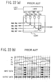
- Figs. 21 and 22 show an arrangement in which reception data are captured by respective latch circuits with respective phases of the multi-phase clocks and processed in the LSI as parallel data. For out putting, the parallel data are again sequentially output as serial data.
- the generated eight-phase clocks are routed to a reception circuit 1103 where input data are latched through a phase adjustment circuit 1104 by respective F/F (flip-flops). Since the frequency rate of input data is four times the frequency of each of the eight-phase clocks, the respective phases latch different values depending on changes in data.
- a phase comparator 1105 detects the data phase from changing points of the latched data to output a control signal 1106 which then is used in a phase adjustment circuit 1104 so that the edges of the multi-phase clocks will be coincident with those of the data. Since one-half of data latched with the eight-phase clocks is used for detecting an optional phase change point, data detected at four phases, corresponding to every second phases, are output as parallel data.
- the input data assumes values of from D 0 to D 7 per period, the input data are serial/parallel converted every four bits.
- four-phase clocks of from P 0 to P 3 are generated on the transmitting side at the PLL 1202 from the reference clocks 1201.
- the generated four-phase clocks are routed to a transmission circuit 1203 where four parallel data are sequentially output as serial data by four parallel gates adapted to be turned on everyone-fourth period. It is seen from the timing chart that the four parallel data DQ 0 toDQ 7 are converted into output serial data DS 0 to DS 7 .
- the transmission circuits and the multi-phase clock generating circuits are used frequently at a ratio of 1:1, that is one transmission circuit is used for one multi-phase clock generating circuit.
- the present invention provides a technical configuration which is basically as defined hereinbelow.
- the present invention provides a clock signal control circuit, as its first aspect, wherein multi-phase clock signals are caused to interact to average out respective phase error components of the clock signals as the phases of the respective clock signals are kept.
- the present invention provides a clock signal control circuit, as its second aspect comprising a plurality of averaging circuits.
- Each of averaging circuits causes multi-phase clock signals to interact to average out respective phase error components of the clock signals as the phases of the respective clock signals are kept.
- the averaging circuits are grouped into a plurality of sets of averaging circuits, wherein each of the averaging circuit sets effects averaging in different states from one another.
- the present invention provides a clock signal control circuit, as its third aspect, in which phase errors of n pulses having different phase errors are averaged out to produce n pulses having averaged phase errors, wherein two or more gates arranged in parallel are provided and outputs of the sates are interconnected to form a unit averaging circuit for averaging phase errors of two or more pulses input to the gates, n of the unit averaging circuits are provided to constitute an averaging circuit set for averaging phase errors of the n pulses, and wherein 1og 2 n stages of the averaging circuit sets are provided, there being a phase inverting circuit provided at an input of each averaging circuit of a first one of the averaging circuit sets fed with the n pulses.
- the present invention provides the clock signal control circuit, as its fourth aspect, wherein the n pulses are supplied to two different unit averaging circuits of the first averaging circuit set, and wherein outputs of the unit averaging circuits of the first averaging circuit set are each fed to two different unit averaging circuits of a second averaging circuit set provided downstream of the first averaging circuit set.
- the present invention provides a clock signal control circuit, as another aspect, wherein outputs of respective unit averaging circuits of the averaging circuit set of a previous stage are fed to two different unit averaging circuits of the averaging circuit set provided downstream of the averaging circuit set of the previous stage.
- the present invention provides a clock signal control circuit, as yet a further aspect, wherein values of the k in the respective averaging circuit sets are different from one averaging circuit set to another.
- the present invention provides a clock signal control circuit, as yet another aspect, wherein, in the respective unit averaging circuits of at least one of the averaging circuit sets, signals with phases differing by ⁇ radians are averaged out.
- the present invention provides a clock signal control circuit, as a further aspect, wherein each unit averaging circuit of at least one of the averaging circuit sets averages out signals having phases different by ⁇ /2 radians from one another.
- the present invention provides a clock signal control circuit, as still another aspect. wherein each unit averaging circuit of at least one of the averaging circuit sets averages out signals having phases neighboring (adjacent) to one another.
- the present invention provides a clock signal control circuit, as yet a further aspect, in which phase errors of n pulses having different phase errors are averaged out to produce n pulses having averaged phase errors, wherein a unit averaging circuit is formed which comprises a first differential pair, a load of each transistor of the first differential pair and a second differential pair connected in parallel with the first differential pair, each of the first and second differential pairs being fed with pulse signals having phases different from each other by ⁇ radians to average out the phase errors of four impulses input to the first and second differential pairs, n/2 of the unit averaging circuits being provided to constitute an averaging circuit set for averaging out the phase errors of the n pulses, and wherein there are provided log 2 (n/2) stages of the averaging circuit sets.
- the present invention provides a clock signal control circuit, as yet another aspect, wherein the n pulses are fed to two different unit averaging circuits of a first one of the unit averaging circuits, and wherein outputs of respective unit averaging circuits of the first averaging circuit set are each fed to two different unit averaging circuits of a second one of the unit averaging circuits provided downstream of the first averaging circuit set.
- the present invention provides a clock signal control circuit, as still another aspect, wherein outputs of respective unit averaging circuits of the upstream side averaging circuit set are each fed to different two of the unit averaging circuits provided downstream of the upstream side averaging circuit sets.
- the present invention provides a clock signal control circuit, as yet a further aspect, in which phase errors of n pulses having different phase errors are averaged out to produce n pulses having averaged phase errors, wherein a plurality of gates connected in parallel with one another are provided, outputs of the plural gates are interconnected to constitute a first unit averaging circuit adapted for averaging out phase errors of two or more pulses input to the gates, and a plurality of such first unit averaging circuits are provided to constitute a first averaging circuit set, and wherein a second unit averaging circuit is formed which comprises a first differential pair, a load of each transistor of the first differential pair and a second differential pair connected in parallel with the first differential pair, each of the first and second differential pairs being fed with pulse signals having phases different from each other by ⁇ radians to average out the phase errors of four pulses fed to the first and second differential pairs, there being provided n/2 second unit averaging circuits to constitute a second averaging circuit set.
- the present invention provides a clock signal control circuit, as another aspect, in which phase errors of n pulses having different phase errors are averaged out to produce n pulses having averaged phase errors, wherein a first unit averaging circuit is formed which comprises a first differential pair, a load of each transistor of the first differential pair and a second differential pair connected in parallel with the first differential pair, each of the first and second differential pairs being fed with pulse signals having phases different from each other by ⁇ radians to average out the phase errors of four impulses fed to the first and second differential pairs,
- the present invention also provides a data transmission apparatus, in its first aspect, wherein multi-phase clocks generated in a multi-phase generating circuit are fed to a first device having phase error averaging circuit to average out phase errors of the multi-phase clocks as respective phases of the multi-phase clocks are kept, and wherein output of the phase error averaging circuit of the first device is fed to a second device having another phase error averaging circuit for averaging out phase errors of the multi-phase clocks under the condition that respective phases of the multi-phase clocks fed to the second device are kept.
- the present invention also provides a data transmission apparatus, in its second aspect, wherein multi-phase clocks generated in a multi-phase generating circuit are fed to a first device having phase error averaging circuit to average out phase errors of the multi-phase clocks as respective phases of the multi-phase clocks are kept, and wherein multi-phase clocks generated in the multi-phase generating circuit are fed to a second device having another phase error averaging circuit to average out phase errors of the multi-phase clocks under the condition that respective phases of the multi-phase clocks are kept.
- the present invention provides a data transmission apparatus, in its third aspect, wherein the phase error averaging circuit is provided in a transmission device of a data transmission apparatus.
- the present invention provides a data transmission apparatus, in its fourth aspect, wherein the phase error averaging circuit is provided in a reception device of a data transmission apparatus.
- a method for controlling clock signals comprises: providing multi-phase clock signals having phase errors, and
- phase error averaging circuit as a clock signal control circuit according to the present invention, signal paths of n multi-phase clock signals P 0 to P n , having different phase differences, are arranged in parallel, the respective signals are input to a phase error averaging circuit which then averages out phase errors of the respective clock signals to output resulting multi-phase clock signals Q 0 to Q n .
- Figs. 1 to 7 show a first specified example of a phase error averaging circuit as a clock signal control circuit according to the present invention.
- a clock signal control circuit wherein multi-phase clock signals are caused to interact to average out respective phase error components of said clock signals as the phases of the respective clock signals are kept.
- a pulse signal phase error averaging circuit in which phase errors of n pulses having different phase errors are averaged out to produce n pulses having averaged phase errors, wherein two or more gates 201a, 201b arranged in parallel are provided and outputs of the gates are interconnected to form a unit averaging circuit 201 for averaging phase errors of two or more pulses input to the gates, n of the unit averaging circuits are provided to constitute an averaging circuit set, for averaging phase errors of then pulses, 1og 2 n stages of the averaging circuit sets are provided, there being a phase inverting circuit provided at an input of each averaging circuit of a first one of the averaging circuit 10 sets fed with the n pulses.
- a pulse signal phase error averaging circuit wherein the n pulses are entered to two different unit averaging circuits of the first averaging circuit set 10; and wherein outputs of the unit averaging circuits of the first averaging circuit set 10 are fed to two different unit averaging circuits of a second averaging circuit set 20 provided downstream of the first averaging circuit set 10.
- pulse signal phase error averaging circuit wherein outputs of respective unit averaging circuits of the averaging circuit set 10 of a previous stage (upstream) are fed to two different unit averaging circuits of the averaging circuit set 20 provided downstream of the averaging circuit set 10 of the previous stage.
- pulse signal phase error averaging circuit wherein, in the respective unit averaging circuits of at least one of the averaging circuit sets, signals with phases differing by ⁇ radian are averaged out.
- each unit averaging circuit of at least one of the averaging circuit sets averages out signals having phases different by ⁇ /2 radian from one another.
- each unit averaging circuit of at least one of the averaging circuit sets averages out signals having phases adjacent to one another.
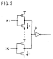
- the averaging circuit includes two inverters, output sides of which are interconnected and an averaging signal is acquired from an output of the two inverters, as shown in Fig. 2.
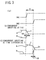
- An output signal of the averaging circuit has a time component of T (phase difference) ⁇ 1/2 where T is the phase difference of the two input signals.
- a quantity of delay after two inputs are fed to the averaging circuit with a time difference of T (phase difference) is assumed to be t B (Fig. 3c).
- the electrical quantity to be charged or discharged in order to invert the next stage of the averaging circuit is Q. Initially, the electrical charge Q is extracted with a current i of the averaging circuit and, after lapse of time T, the electrical charge Q is extracted with a current 2i.
- the left side (Q - Ti) denotes the residual electrical charge that needs to be extracted in order to invert the next stage which remains uninverted during the time T during which only one inverter is in operation.
- the averaging circuit has a time component equal to 1/2 of the time difference of two inputs.
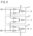
- FIG. 4 A circuit shown in Fig. 4 is considered for aiding the understanding.
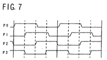
- P 0 to P 3 are four clock signals input to an averaging circuit. Referring to Fig.7, the clock signals are delayed in phase each by ⁇ /4 in the order of P 0 to P 3 , with these clock signals P 0 to P 3 having phase errors of E 0 to E 3 , respectively.
- the clock signal P 0 is input to an averaging circuit 201-10, with an inverted signal thereof being input to an averaging circuit 201-12.
- the clock signal P 1 is input to an averaging circuit 201-11, with an inverted signal thereof being input to an averaging circuit 201-13.
- the clock signal P 2 is input to an averaging circuit 201-12, with an inverted signal thereof being input to an averaging circuit 201-10.
- the clock signal P 3 is input to an averaging circuit 201-13, with an inverted signal thereof being input to an averaging circuit 201-11.
- the averaging circuits 201-10 to 201-13 make up a first averaging circuit set, this circuit set averaging the phase errors of clock signals having 180° phase difference to each other.
- An output signal of the averaging circuit 201-10 is input to averaging circuits 201-20 and 201-21.
- An output signal of the averaging circuit 201-11 is input to averaging circuits 201-21 and 201-22.
- An output signal of the averaging circuit 201-12 is input to averaging circuits 201-22 and 201-23.
- an output signal of the averaging circuit 201-13 is input to averaging circuits 201-23 and 201-20.
- a clock Q 2 having a phase error of respective clock signals averaged out is issued.
- a clock Q 3 having a phase error of respective clock signals averaged out is issued.
- the averaging circuits 201-20 to 201-23 make up a second averaging circuit set 20, this circuit set averaging out the phase errors of the clock signals having neighboring (adjacent) phases to each other.
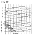
- Figs. 8 to 11 show a second specified example of the present invention, with Fig. 8 being a block diagram, Fig. 9 schematically showing the phase relation of the respective clocks and the mode of averaging out, Fig. 10 showing a waveform diagram and Fig. 11 showing the result of simulation.
- This specified example uses eight-phase clocks.
- a first averaging circuit set 100 averages out diagonal clock signals (180°)
- a second averaging circuit set 200 averages out neighboring clock signals (45°)
- a third averaging circuit set 300 averages out every second clock signals (90°).
- Fig. 9 schematically shows the averaging modes.
- P 0 to P 7 denote eight phase input clocks. These clocks are arrayed circularly to indicate the relation (states) of the respective phases.
- the averaging is made between diagonal phases (180°), neighboring phases (45°) and every second phases (90°), as described above, there is no limitation to the order in which the averaging is made.
- the errors of the respective phases are E 0 to E 7 phase errors of the clock signals of the respective phases passed through this circuit are as follows:
- Outputs of the second averaging circuit set 200 are:
- Outputs of the third averaging circuit set 300 are:
- phase errors are progressively averaged out from one circuit set to another, such that ultimately the entire phase components are completely averaged out. If this phase averaging is shown by the timing chart of Fig.10, when the eight-phase input signals P 0 to P 7 are passed through the circuit of Fig.8 to output signals Q 0 to Q 7 , the phase error td of the clock P 2 is equally distributed in an amount of td/8 to each of Q0 to Q 7 .
- Fig.11 shows the result of simulation of this circuit.
- phase error averaging is performed on 1.6n period (622 MHz) eight-phase clocks (ideal phase difference of 200ps).
- the phase error of the input signal with a maximum phase error of 100ps (50ps) is decreased to a phase error of 5ps (2.5%) or less.
- the multi-phase clock signals, containing phase errors, and the multi-phase clock signals, freed of the phase errors are shown in an upper portion and in a lower portion of Fig. 11, respectively.
- the phase error is not reduced completely to zero because of the incomplete averaging circuit. However, if the clocks are passed once again through the present circuit, the phase errors are further reduced to approximately one/tenth.
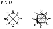
- Figs. 12 and 13 show a third specified example of the present invention. Specifically, Fig. 12a and Fig. 12b show a block diagram and a unit averaging circuit, respectively, and Fig. 13 schematically shows the phase relation of respective clocks and manners (modes) of averaging out the phase errors of the clocks.
- a pulse signal phase averaging circuit 701 in which phase errors of n pulses having different phase errors are averaged out to produce n pulses having averaged phase errors, wherein a unit averaging circuit is formed which comprises a first differential pair S1, a load 810, 811 of each transistor of the first differential pair S1, and a second differential pair S2 connected in parallel with the first differential pair S1, each of the first and second differential pairs S1, S2 being fed with pulse signals having phases different from each other by ⁇ radians to average out the phase errors of four pulses input to the first and second differential pairs S1, S2.
- n/2 of the unit averaging circuits 701 are provided to constitute an averaging circuit set for averaging out the phase errors of the n pulses.
- log 2 (n/2) stages of the averaging circuit sets There are provided log 2 (n/2) stages of the averaging circuit sets.
- pulses are input to two different unit averaging circuits of a first set 400 of the unit averaging circuits and wherein outputs of respective unit averaging circuits of the first averaging circuit set 400 are input to two different unit averaging circuits of a second set 500 of the unit averaging circuits provided downstream of the first averaging circuit set 400.
- pulse signal phase averaging circuit wherein outputs of respective unit averaging circuits of the upstream side averaging circuit set 400 are input to different two of the unit averaging circuits 500 provided downstream of the upstream side averaging circuit set 400.
- the averaging circuit used in this circuitry includes a first differential pair S1, made up of FETs 801, 802, loads 810, 811 of respective transistors of the differential pair S1, and a second differential pair S2, made up of FETs 803, 804, connected in parallel with the first differential pair S1.
- the differential pairs S1, S2 are fed with pulse signals IN1, IN1B; IN2, IN2B, having phases different by ⁇ radians, to average out phase errors of four pulses input to the first differential pair S1 and the second differential pair S2, respectively.
- Fig. 12a shows a block diagram of the third specified example.
- a first differential pair of an averaging circuit 701-11 is fed with clock signals P 0 , P 4 having phases 180° different from each other.
- a second differential pair of the averaging circuit 701-12 is fed with neighboring clock signals P 1 , P 5 having phases 180° different from each other.
- a first differential pair of an averaging circuit 701-12 is fed with clock signals P 1 , P 5 having chases 180° different from each other.
- a second differential pair of the averaging circuit 701-12 is fed with neighboring clock signals P 2 , P 6 having phases 180° different from each other.
- a first differential pair of an averaging circuit 701-13 is fed with clock signals P 2 , P 6 having phases 180° different from each other.
- a second differential pair of the averaging circuit 701-13 is fed with neighboring clock signals P 3 , P 7 having phases 180° different from each other.
- a first differential pair of an averaging circuit 701-14 is fed with clock signals P 3 , P 7 having phases 180° different from each other.
- a second differential pair of the averaging circuit 701-14 is fed with neighboring clock signals P 0 , P 4 having phases 180° different from each other.
- the averaging circuits 701-11 to 701-14 make up a first averaging circuit set 400 to effect averaging.
- a first differential pair of an averaging circuit 701-21 is fed with output signals of the averaging circuit 701-11 having phases 180° different from each other.
- a second differential pair of the averaging circuit 701-21 is fed with output signals of the averaging circuit 701-13 having phases offset 90° from each other.
- a first differential pair of an averaging circuit 701-22 is fed with output signals of the averaging circuit 701-12 having phases 180° different from each other.
- a second differential pair of the averaging circuit 701-22 is fed with output signals of the averaging circuit 701-14 having phases offset 90° from each other.
- a first differential pair of an averaging circuit 701-23 is fed with output signals of the averaging circuit 701-13 having phases 180° different from each other.
- a second differential pair of the averaging circuit 701-23 is fed with output signals of the averaging circuit 701-11 having phases offset 90° from each other.
- a first differential pair of an averaging circuit 701-24 is fed with output signals of the averaging circuit 701-14 having phases 180° different from each other.
- a second differential pair of the averaging circuit 701-24 is fed with output signals of the averaging circuit 701-12 having chases offset 90° from each other.
- the averaging circuits 701-11 to 701-14 make up a first averaging circuit set 400, whilst the averaging circuits 701-21 to 701-24 make up a second averaging circuit set 500.
- the clock signals are passed through the first and second circuit sets with different combinations to effect progressive averaging to average out the phase errors over the entire clock signals as the phase difference of the clock signals is maintained.
- averaging of the multi-clocks is hereinafter explained.
- eight phase clocks are used.
- averaging is made between neighboring phase angles (45°) and diagonally opposite phase angles (135°) and between every second phase angles (90°) and between diagonal angles (180°).
- Fig. 13 schematically shows the relation of averaging.
- P 0 to P 7 denote eight-phase clocks. These clocks are arrayed circularly to indicate the relation (or states) of the respective phases.
- the averaging is made between neighboring phases (45°) and diagonally opposite phases (180°) and between every second phases (90°) and diagonally opposite phases (180°), as described above, there is no limitation to the order in which the averaging is made.
- the errors of the respective phases are E 0 to E 7
- the phase errors of the clock signals of the respective phases, passed through the present circuit are sequentially averaged out, as shown below, such that ultimately the entire phase components are completely averaged out.
- the outputs of the first averaging circuit set 400 are as follows:
- the outputs of the second averaging circuit set 500 are as follows:
- an averaging circuit employing a differential circuit averages the diagonal signals by a sole circuit, thus advantageously reducing the number of stages necessary for full averaging.
- the averaging circuits used in the first and second specified examples and the averaging circuits used in the third specified example may be used in combination.
- a pulse signal phase error averaging circuit arrangement in which phase errors of n pulses having different phase errors are averaged out to produce n pulses having averaged phase errors.
- a plurality of gates connected in parallel with one another are provided, outputs of the plural gates are interconnected to constitute a first unit averaging circuit adapted for averaging out phase errors of two or more pulses input to the gates, and a plurality of such first unit averaging circuits are provided to constitute a first averaging circuit set.
- a second unit averaging circuit which comprises a first differential pair, a load of each transistor of the first differential pair and a second differential pair connected in parallel with the first differential pair, each of the first and second differential pairs being fed with pulse signals having the phases different from each other by ⁇ radians to average out the phase errors of four pulses input to the first and second differential pairs.
- n/2 second unit averaging circuits may constitute a second averaging circuit set, whilst respective outputs of the unit averaging circuits of the first averaging circuit set may be input to the unit averaging circuit of the second averaging circuit set.
- a pulse signal phase error averaging circuit in which phase errors of n pulses having different phase errors are averaged out to produce n pulses having averaged phase errors.
- a first unit averaging circuit is formed which comprises a first differential pair, a load of each transistor of the first differential pair and a second differential pair connected in parallel with the first differential pair, each of the first and second differential pairs being fed with pulse signals having the phases different from each other by ⁇ radians to average out the phase errors of four impulses input to the first and second differential pairs, n/2 of the unit averaging circuits being provided to constitute an averaging circuit set for averaging out the phase errors of four pulses fed to the first and second differential pairs to constitute a first averaging circuit set.
- a second unit averaging circuit which comprises a plurality of sates arranged in parallel with one another, outputs of the plural gates being interconnected to average out phase errors of two or more pulses input to the gates, a plurality of the second unit averaging circuits being provided to constitute a second averaging circuit set, respective outputs of the unit averaging circuits of the first averaging circuit set being adapted to be input to the unit averaging circuits of the second averaging circuit set.
- the present invention is applied to a digital PLL circuit adapted for generating multi-phase clocks or multiplied clocks.
- the present invention is applied to a circuit of Fig. 21 in which reception data are captured in separate latch circuits at respective phases of the multi-phase clocks and processed as parallel data in the LSI.
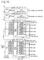
- Fig. 15 shows a block diagram of the present specified example.
- phase error averaging circuits 1312, 1322. 1332 of the eight-phase clock configuration according to the present invention replace PLLs of Fig. 21 are provided and the phase error averaging circuits are connected in tandem with the circuit of the configuration of Fig. 21 as an inchoative point.
- plural reception circuits can be control led by a single PLL with a lesser phase-to-phase errors.
- a data transmission apparatus of the fifth specified example is constructed so that multi-phase clocks generated in a multi-phase generating circuit are routed to a first device having phase error averaging circuit for averaging out phase errors of the multi-phase clocks as respective phases of the multi-phase clocks are kept, and so that
- the present invention is applied to a circuit of Fig. 22 in which parallel data are sequentially output with multi-phase clocks as serial data.
- Fig. 16 shows a block diagram of the present specified example.
- phase error averaging circuits 1404, 1414 and 1424 of the four-phase clock configuration replace PLLs of Fig. 22, whilst a PLL 1402 adapted for generating multi-phase clocks is arranged to supply the multi-phase clocks to the respective phase error averaging circuits.
- the data transmission apparatus of the sixth specified example is constructed so that multi-phase clocks generated in a multi-phase generating circuit are routed to a first device having phase error averaging circuit for averaging out phase errors of the multi-phase clocks as respective phases of the multi-phase clocks are kept, and so that multi-phase clocks generated in the multi-phase generating circuit are routed to a second device having another phase error averaging circuit for averaging out phase errors of the multi-phase clocks as respective phases of the multi-phase clocks are kept.
- clock phase interval deviation produced due to manufacturing fluctuations of clock drivers or fluctuations in the wiring resistance can be corrected in the distribution of multiple phase clocks, it is possible to distribute multi-phase clock signals over a wide range or distance.
- the multi-phase clocks generated by e.g., digital PLL circuits, it is possible to correct deviations in the clock phase intervals produced due to quantization errors of the digital PLL circuits.
- a multi-phase clock generating circuit such as a multi-phase PLL circuit
- a clock signal control circuit it is possible to reduce the number of the multi-phase clock generating circuits to construct the circuit more readily and inexpensively.
Landscapes
- Physics & Mathematics (AREA)
- Nonlinear Science (AREA)
- Engineering & Computer Science (AREA)
- Computer Networks & Wireless Communication (AREA)
- Signal Processing (AREA)
- Synchronisation In Digital Transmission Systems (AREA)
- Manipulation Of Pulses (AREA)
- Pulse Circuits (AREA)
- Stabilization Of Oscillater, Synchronisation, Frequency Synthesizers (AREA)
Abstract
Description
wherein, in each of the unit averaging circuits of at least one averaging circuit set in the plural averaging circuit sets, signals differing in phase by π/2k radians, where k=0,1,2,··· are averaged out.
wherein each unit averaging circuit of at least one of the averaging circuit sets averages out signals having phases neighboring (adjacent) to one another.
wherein the phase error averaging circuit is provided in a reception device of a data transmission apparatus.
Claims (20)
- A clock signal control circuit
whereinmulti-phase clock signals are caused to interact to average out respective phase error components of said clock signals as the phases of the respective clock signals are kept. - A clock signal control circuitcomprising a plurality of averaging circuits,each of said averaging circuits causing multi-phase clock signals to interact to average out respective phase error components of said clock signals as the phases of the respective clock signals are kept,said averaging circuits being grouped into a plurality of sets of averaging circuits,
wherein each of said averaging circuit sets effects averaging in a different state from one another. - A clock signal control circuit in which phase errors of n pulses having different phase errors are averaged out to produce n pulses having averaged phase errors;
whereintwo or more gates arranged in parallel are provided and outputs of said gates are interconnected to form a unit averaging circuit for averaging phase errors of two or more pulses input to said gates;n of said unit averaging circuits are provided to constitute an averaging circuit set for averaging phase errors of said n pulses;log2n stages of said averaging circuit sets are provided;there being a phase inverting circuit provided at an input of each averaging circuit of a first one of said averaging circuit sets fed with said n pulses. - The clock signal control circuit as defined in claim 3
whereinsaid n pulses are supplied to two different unit averaging circuits of the first averaging circuit set; and whereinoutputs of said unit averaging circuits of said first averaging circuit set are each fed to two different unit averaging circuits of a second averaging circuit set provided downstream of said first averaging circuit set. - The clock signal control circuit as defined in claim 4
whereinoutputs of said unit averaging circuits of the averaging circuit set of a previous stage are respectively fed to two different unit averaging circuits of the averaging circuit set provided downstream of said averaging circuit set of the previous stage. - The clock signal control circuit as defined in claim 3
whereinin each of the unit averaging circuits of at least one averaging circuit set in said plural averaging circuit sets, signals differing in phase by π/2k radians, where k=0,1,2,··· are averaged out. - The clock signal control circuit as defined in claim 6
whereinvalues of said k in the respective averaging circuit sets are different from one averaging circuit set to another. - The clock signal control circuit as defined in claim 3
whereinin the respective unit averaging circuits of at least one of said averaging circuit sets, signals with phases differing by π radians are averaged out. - The clock signal control circuit as defined in any one of claims 3 to 8
whereineach unit averaging circuit of at least one of said averaging circuit sets averages out signals having phases different by π/2 radians from one another. - The clock signal control circuit as defined in claim 3
whereineach unit averaging circuit of at least one of said averaging circuit sets averages out signals having phases adjacent to one another. - A clock signal control circuit in which phase errors of n pulses having different phase errors are averaged out to produce n pulses having averaged phase errors;
whereina unit averaging circuit is formed which comprises a first differential pair, a load of each transistor of said first differential pair and a second differential pair connected in parallel with said first differential pair,each of said first and second differential pairs being fed with pulse signals having phases different from each other by π radians to average out the phase errors of four impulses input to said first and second differential pairs,n/2 of said unit averaging circuits being provided to constitute an averaging circuit set for averaging out the phase errors of said n pulses, and
wherein there are provided log2(n/2) stages of said averaging circuit sets. - The clock signal control circuit as defined in claim 11
whereinsaid n pulses are fed to two different unit averaging circuits of a first one of said unit averaging circuits, and whereinoutputs of respective unit averaging circuits of said first averaging circuit set are each fed to two different unit averaging circuits of a second one of said unit averaging circuits provided downstream of said first averaging circuit set. - The clock signal control circuit as defined in claim 12
whereinoutputs of respective unit averaging circuits of said upstream side averaging circuit set are each fed to different two of said unit averaging circuits provided downstream of said upstream side averaging circuit sets. - A clock signal control circuit in which phase errors of n pulses having different phase errors are averaged out to produce n pulses having averaged phase errors;
whereina plurality of gates connected in parallel with one another are provided, outputs of said plural gates are interconnected to constitute a first unit averaging circuit adapted for averaging out phase errors of two or more pulses input to said gates, and a plurality of said first unit averaging circuits are provided to constitute a first averaging circuit set; and whereina second unit averaging circuit is formed which comprises a first differential pair, a load of each transistor of said first differential pair and a second differential pair connected in parallel with said first differential pair, each of said first and second differential pairs being fed with pulse signals having phases different from each other by π radians to average out phase errors of four pulses fed to said first and second differential pairs,there being provided n/2 second unit averaging circuits to constitute a second averaging circuit set;respective outputs of the unit averaging circuits of said first averaging circuit set being fed to the unit averaging circuit of said second averaging circuit set. - A clock signal control circuit in which phase errors of n pulses having different phase errors are averaged out to produce n pulses having averaged phase errors;
whereina first unit averaging circuit is formed which comprises a first differential pair, a load of each transistor of said first differential pair and a second differential pair connected in parallel with said first differential pair, each of said first and second differential pairs being fed with pulse signals having phases different from each other by π radians to average out the phase errors of four impulses fed to said first and second differential pairs,n/2 of said unit averaging circuits being provided to constitute an averaging circuit set for averaging out the phase errors of four pulses fed to said first and second differential pairs to constitute a first averaging circuit set;a second unit averaging circuit is formed which comprises a plurality of gates arranged in parallel with one another, outputs of said plural gates being interconnected to average out phase errors of two or more pulses fed to said gates, a plurality of said second unit averaging circuits being provided to constitute a second averaging circuit set;respective outputs of said unit averaging circuits of said first averaging circuit set being adapted to be fed to said unit averaging circuits of said second averaging circuit set. - A data transmission apparatus
whereinmulti-phase clocks generated in a multi-phase generating circuit are fed to a first device having phase error averaging circuit to average out phase errors of said multi-phase clocks as respective phases of said multi-phase clocks are kept, and whereinoutput of said phase error averaging circuit of said first device being fed to a second device having another phase error averaging circuit to average out phase errors of said multi-phase clocks under the condition that respective phases of said multi-phase clocks fed to said second device are kept. - A data transmission apparatus
whereinmulti-phase clocks generated in a multi-phase generating circuit are fed to a first device having a phase error averaging circuit to average out phase errors of said multi-phase clocks under the condition that respective phases of said multi-phase clocks are kept, and whereinmulti-phase clocks generated in said multi-phase generating circuit are fed to a second device having another phase error averaging circuit to average out phase errors of said multi-phase clocks under the condition that respective phases of said multi-phase clocks are kept. - The data transmission apparatus as defined in claim 16
whereinsaid phase error averaging circuit is provided in a transmission device of a data transmission apparatus. - The data transmission apparatus as defined in claim 16
whereinsaid phase error averaging circuit is provided in a reception device of a data transmission apparatus. - A method for controlling clock signals comprising:providing multi-phase clock signals having phase errors, andcausing said multi-phase clock signals to interact with one another to average out phase error components of said lock signals, with the phases of said clock signals being kept.
Applications Claiming Priority (2)
| Application Number | Priority Date | Filing Date | Title |
|---|---|---|---|
| JP17838299A JP3573661B2 (en) | 1999-06-24 | 1999-06-24 | Clock signal control method and circuit and data transmission device using the same |
| JP17838299 | 1999-06-24 |
Publications (3)
| Publication Number | Publication Date |
|---|---|
| EP1063810A2 true EP1063810A2 (en) | 2000-12-27 |
| EP1063810A3 EP1063810A3 (en) | 2004-11-24 |
| EP1063810B1 EP1063810B1 (en) | 2007-02-14 |
Family
ID=16047524
Family Applications (1)
| Application Number | Title | Priority Date | Filing Date |
|---|---|---|---|
| EP00250209A Expired - Lifetime EP1063810B1 (en) | 1999-06-24 | 2000-06-24 | Clock signal control method and circuit and data transmitting apparatus employing the same |
Country Status (8)
| Country | Link |
|---|---|
| US (1) | US6340910B1 (en) |
| EP (1) | EP1063810B1 (en) |
| JP (1) | JP3573661B2 (en) |
| KR (1) | KR100411441B1 (en) |
| CN (1) | CN100399735C (en) |
| CA (1) | CA2312106A1 (en) |
| DE (1) | DE60033339T2 (en) |
| TW (1) | TW454387B (en) |
Cited By (1)
| Publication number | Priority date | Publication date | Assignee | Title |
|---|---|---|---|---|
| DE102004036283B4 (en) * | 2003-07-28 | 2009-10-22 | Nec Electronics Corp., Kawasaki | Phase interpolator circuitry for reducing clock skew |
Families Citing this family (16)
| Publication number | Priority date | Publication date | Assignee | Title |
|---|---|---|---|---|
| JP3519693B2 (en) * | 2000-04-04 | 2004-04-19 | 松下電器産業株式会社 | Multi-phase clock signal generation circuit |
| JP3838890B2 (en) * | 2001-08-21 | 2006-10-25 | Necエレクトロニクス株式会社 | Semiconductor integrated circuit and design method thereof |
| JP3849485B2 (en) | 2001-10-18 | 2006-11-22 | セイコーエプソン株式会社 | Pulse processing circuit and frequency multiplication circuit |
| JP3960271B2 (en) * | 2003-07-02 | 2007-08-15 | ソニー株式会社 | Phase error determination method, digital PLL device |
| JP4703997B2 (en) * | 2004-09-28 | 2011-06-15 | 富士通セミコンダクター株式会社 | Semiconductor integrated circuit |
| KR100641360B1 (en) | 2004-11-08 | 2006-11-01 | 삼성전자주식회사 | Delay locked loop and semiconductor memory device comprising the same |
| TWI265703B (en) * | 2004-12-22 | 2006-11-01 | Prolific Technology Inc | A system and method of clock architecture of oversampling high speed clock/data recovery |
| KR100809714B1 (en) | 2007-01-03 | 2008-03-06 | 삼성전자주식회사 | Multiphase Generation Method and Appropriate Device |
| KR20090045495A (en) | 2007-11-02 | 2009-05-08 | 주식회사 하이닉스반도체 | Clock control circuit and data alignment circuit including the same |
| KR100904236B1 (en) | 2007-11-06 | 2009-06-25 | 주식회사 부방테크론 | IH circuit control unit to ensure minimum switching off time |
| KR100967103B1 (en) * | 2008-06-30 | 2010-07-05 | 주식회사 하이닉스반도체 | Clock Generation Circuit and Clock Generation Method |
| JP5442723B2 (en) | 2009-05-13 | 2014-03-12 | パナソニック株式会社 | Hybrid data transmission circuit |
| DE112010004514B4 (en) * | 2009-11-20 | 2021-01-07 | Keysight Technologies Singapore (Sales) Pte. Ltd. | Method, system and computer program product for measuring a data transmission from a first device to a second device |
| JP5910383B2 (en) * | 2012-07-19 | 2016-04-27 | 株式会社ソシオネクスト | Skew reduction circuit |
| CA3061786C (en) | 2018-11-20 | 2024-03-19 | Square Grove Llc | Vertically adjustable desk with under-carriage mounting system |
| CN112462848B (en) * | 2020-12-07 | 2024-04-09 | 深圳供电局有限公司 | Clock deviation correction method, device and computer equipment |
Family Cites Families (11)
| Publication number | Priority date | Publication date | Assignee | Title |
|---|---|---|---|---|
| JPS594900B2 (en) * | 1979-09-03 | 1984-02-01 | 日本電気株式会社 | clock recovery circuit |
| US4669024A (en) * | 1985-10-23 | 1987-05-26 | Westinghouse Electric Corp. | Multiphase frequency selective phase locked loop with multiphase sinusoidal and digital outputs |
| US4963839A (en) * | 1989-09-01 | 1990-10-16 | Westinghouse Electric Corp. | Wide bandwidth phase locked loop circuit with sliding window averager |
| JP3315134B2 (en) * | 1991-09-05 | 2002-08-19 | 株式会社日立製作所 | Multi-track phase synchronizer |
| JP3321926B2 (en) * | 1993-09-17 | 2002-09-09 | 株式会社日立製作所 | Self-synchronous semiconductor integrated circuit device |
| JP2806863B2 (en) * | 1996-02-27 | 1998-09-30 | 日本電気エンジニアリング株式会社 | Bit synchronization circuit |
| JP3125699B2 (en) | 1996-12-25 | 2001-01-22 | 日本電気株式会社 | Data synchronization circuit |
| KR100240278B1 (en) * | 1997-02-14 | 2000-01-15 | 김영환 | Clock Generation Circuit for LCD Driver |
| JP3678541B2 (en) * | 1997-06-12 | 2005-08-03 | 富士通株式会社 | Phase correction circuit, phase correction DLL circuit, multi-phase clock generation DLL circuit, and semiconductor device |
| JP2978856B2 (en) * | 1997-09-29 | 1999-11-15 | 山形日本電気株式会社 | Horizontal scanning pulse signal control circuit |
| US5923613A (en) * | 1998-03-18 | 1999-07-13 | Etron Technology, Inc. | Latched type clock synchronizer with additional 180°-phase shift clock |
-
1999
- 1999-06-24 JP JP17838299A patent/JP3573661B2/en not_active Expired - Fee Related
-
2000
- 2000-06-15 TW TW089111708A patent/TW454387B/en not_active IP Right Cessation
- 2000-06-23 KR KR10-2000-0034684A patent/KR100411441B1/en not_active Expired - Fee Related
- 2000-06-23 CN CNB001094319A patent/CN100399735C/en not_active Expired - Fee Related
- 2000-06-23 CA CA002312106A patent/CA2312106A1/en not_active Abandoned
- 2000-06-24 EP EP00250209A patent/EP1063810B1/en not_active Expired - Lifetime
- 2000-06-24 DE DE60033339T patent/DE60033339T2/en not_active Expired - Lifetime
- 2000-06-26 US US09/603,211 patent/US6340910B1/en not_active Expired - Lifetime
Cited By (1)
| Publication number | Priority date | Publication date | Assignee | Title |
|---|---|---|---|---|
| DE102004036283B4 (en) * | 2003-07-28 | 2009-10-22 | Nec Electronics Corp., Kawasaki | Phase interpolator circuitry for reducing clock skew |
Also Published As
| Publication number | Publication date |
|---|---|
| TW454387B (en) | 2001-09-11 |
| KR100411441B1 (en) | 2003-12-18 |
| CN100399735C (en) | 2008-07-02 |
| KR20010021020A (en) | 2001-03-15 |
| JP2001007686A (en) | 2001-01-12 |
| CA2312106A1 (en) | 2000-12-24 |
| DE60033339D1 (en) | 2007-03-29 |
| DE60033339T2 (en) | 2007-10-31 |
| CN1279550A (en) | 2001-01-10 |
| US6340910B1 (en) | 2002-01-22 |
| JP3573661B2 (en) | 2004-10-06 |
| EP1063810B1 (en) | 2007-02-14 |
| EP1063810A3 (en) | 2004-11-24 |
Similar Documents
| Publication | Publication Date | Title |
|---|---|---|
| EP1063810A2 (en) | Clock signal control method and circuit and data transmitting apparatus employing the same | |
| KR102599904B1 (en) | Multiphase clock duty cycle and skew measurement and correction | |
| US8363773B2 (en) | Digital phase interpolation control for clock and data recovery circuit | |
| US5818890A (en) | Method for synchronizing signals and structures therefor | |
| EP1599943B1 (en) | Clock and data recovery phase-locked loop and high-speed phase detector architecture | |
| US5457718A (en) | Compact phase recovery scheme using digital circuits | |
| US8674736B2 (en) | Clock synchronization circuit | |
| EP1139201A2 (en) | Clock control circuit and clock control method | |
| US7590211B1 (en) | Programmable logic device integrated circuit with communications channels having sharing phase-locked-loop circuitry | |
| US9287883B2 (en) | Multi-lane re-timer circuit and multi-lane reception system | |
| US7482841B1 (en) | Differential bang-bang phase detector (BBPD) with latency reduction | |
| US8624630B2 (en) | Clock and data recovery system, phase adjusting method, and phasedetector | |
| US8023605B2 (en) | Oversampling circuit and oversampling method | |
| US11777475B2 (en) | Multiple adjacent slicewise layout of voltage-controlled oscillator | |
| US7245240B1 (en) | Integrated circuit serializers with two-phase global master clocks | |
| US7323918B1 (en) | Mutual-interpolating delay-locked loop for high-frequency multiphase clock generation | |
| US20020006177A1 (en) | Parallel data interface | |
| US10659059B2 (en) | Multi-phase clock generation circuit | |
| US10033525B2 (en) | Transmission device and signal processing method | |
| US8311170B2 (en) | Data transfer system | |
| KR100258086B1 (en) | High speed digital data retiming device | |
| JP7169781B2 (en) | Signal processing apparatus and method | |
| US9793900B1 (en) | Distributed multi-phase clock generator having coupled delay-locked loops |
Legal Events
| Date | Code | Title | Description |
|---|---|---|---|
| PUAI | Public reference made under article 153(3) epc to a published international application that has entered the european phase |
Free format text: ORIGINAL CODE: 0009012 |
|
| AK | Designated contracting states |
Kind code of ref document: A2 Designated state(s): AT BE CH CY DE DK ES FI FR GB GR IE IT LI LU MC NL PT SE |
|
| AX | Request for extension of the european patent |
Free format text: AL;LT;LV;MK;RO;SI |
|
| RAP1 | Party data changed (applicant data changed or rights of an application transferred) |
Owner name: NEC ELECTRONICS CORPORATION |
|
| PUAL | Search report despatched |
Free format text: ORIGINAL CODE: 0009013 |
|
| AK | Designated contracting states |
Kind code of ref document: A3 Designated state(s): AT BE CH CY DE DK ES FI FR GB GR IE IT LI LU MC NL PT SE |
|
| AX | Request for extension of the european patent |
Extension state: AL LT LV MK RO SI |
|
| 17P | Request for examination filed |
Effective date: 20041130 |
|
| 17Q | First examination report despatched |
Effective date: 20050322 |
|
| AKX | Designation fees paid |
Designated state(s): DE FR GB IT |
|
| GRAP | Despatch of communication of intention to grant a patent |
Free format text: ORIGINAL CODE: EPIDOSNIGR1 |
|
| GRAS | Grant fee paid |
Free format text: ORIGINAL CODE: EPIDOSNIGR3 |
|
| GRAA | (expected) grant |
Free format text: ORIGINAL CODE: 0009210 |
|
| AK | Designated contracting states |
Kind code of ref document: B1 Designated state(s): DE FR GB IT |
|
| REG | Reference to a national code |
Ref country code: GB Ref legal event code: FG4D |
|
| REF | Corresponds to: |
Ref document number: 60033339 Country of ref document: DE Date of ref document: 20070329 Kind code of ref document: P |
|
| ET | Fr: translation filed | ||
| PLBE | No opposition filed within time limit |
Free format text: ORIGINAL CODE: 0009261 |
|
| STAA | Information on the status of an ep patent application or granted ep patent |
Free format text: STATUS: NO OPPOSITION FILED WITHIN TIME LIMIT |
|
| 26N | No opposition filed |
Effective date: 20071115 |
|
| PG25 | Lapsed in a contracting state [announced via postgrant information from national office to epo] |
Ref country code: IT Free format text: LAPSE BECAUSE OF FAILURE TO SUBMIT A TRANSLATION OF THE DESCRIPTION OR TO PAY THE FEE WITHIN THE PRESCRIBED TIME-LIMIT Effective date: 20070214 |
|
| REG | Reference to a national code |
Ref country code: FR Ref legal event code: CD |
|
| REG | Reference to a national code |
Ref country code: DE Ref legal event code: R082 Ref document number: 60033339 Country of ref document: DE Representative=s name: STORK BAMBERGER PATENTANWAELTE, DE |
|
| REG | Reference to a national code |
Ref country code: DE Ref legal event code: R081 Ref document number: 60033339 Country of ref document: DE Owner name: RENESAS ELECTRONICS CORPORATION, KAWASAKI-SHI, JP Free format text: FORMER OWNER: NEC ELECTRONICS CORP., KAWASAKI, KANAGAWA, JP Effective date: 20120828 Ref country code: DE Ref legal event code: R081 Ref document number: 60033339 Country of ref document: DE Owner name: RENESAS ELECTRONICS CORPORATION, JP Free format text: FORMER OWNER: NEC ELECTRONICS CORP., KAWASAKI, JP Effective date: 20120828 Ref country code: DE Ref legal event code: R082 Ref document number: 60033339 Country of ref document: DE Representative=s name: STORK BAMBERGER PATENTANWAELTE, DE Effective date: 20120828 |
|
| PGFP | Annual fee paid to national office [announced via postgrant information from national office to epo] |
Ref country code: GB Payment date: 20130619 Year of fee payment: 14 Ref country code: DE Payment date: 20130619 Year of fee payment: 14 |
|
| PGFP | Annual fee paid to national office [announced via postgrant information from national office to epo] |
Ref country code: FR Payment date: 20130624 Year of fee payment: 14 |
|
| REG | Reference to a national code |
Ref country code: DE Ref legal event code: R119 Ref document number: 60033339 Country of ref document: DE |
|
| GBPC | Gb: european patent ceased through non-payment of renewal fee |
Effective date: 20140624 |
|
| REG | Reference to a national code |
Ref country code: FR Ref legal event code: ST Effective date: 20150227 |
|
| REG | Reference to a national code |
Ref country code: DE Ref legal event code: R119 Ref document number: 60033339 Country of ref document: DE Effective date: 20150101 |
|
| PG25 | Lapsed in a contracting state [announced via postgrant information from national office to epo] |
Ref country code: DE Free format text: LAPSE BECAUSE OF NON-PAYMENT OF DUE FEES Effective date: 20150101 |
|
| PG25 | Lapsed in a contracting state [announced via postgrant information from national office to epo] |
Ref country code: FR Free format text: LAPSE BECAUSE OF NON-PAYMENT OF DUE FEES Effective date: 20140630 Ref country code: GB Free format text: LAPSE BECAUSE OF NON-PAYMENT OF DUE FEES Effective date: 20140624 |