EP1061735A2 - Imaging apparatus having a multi port memory - Google Patents
Imaging apparatus having a multi port memory Download PDFInfo
- Publication number
- EP1061735A2 EP1061735A2 EP00112713A EP00112713A EP1061735A2 EP 1061735 A2 EP1061735 A2 EP 1061735A2 EP 00112713 A EP00112713 A EP 00112713A EP 00112713 A EP00112713 A EP 00112713A EP 1061735 A2 EP1061735 A2 EP 1061735A2
- Authority
- EP
- European Patent Office
- Prior art keywords
- read
- signal
- video
- image
- field
- Prior art date
- Legal status (The legal status is an assumption and is not a legal conclusion. Google has not performed a legal analysis and makes no representation as to the accuracy of the status listed.)
- Withdrawn
Links
Images




Classifications
-
- H—ELECTRICITY
- H04—ELECTRIC COMMUNICATION TECHNIQUE
- H04N—PICTORIAL COMMUNICATION, e.g. TELEVISION
- H04N7/00—Television systems
- H04N7/01—Conversion of standards, e.g. involving analogue television standards or digital television standards processed at pixel level
- H04N7/0135—Conversion of standards, e.g. involving analogue television standards or digital television standards processed at pixel level involving interpolation processes
-
- G—PHYSICS
- G11—INFORMATION STORAGE
- G11C—STATIC STORES
- G11C19/00—Digital stores in which the information is moved stepwise, e.g. shift registers
- G11C19/28—Digital stores in which the information is moved stepwise, e.g. shift registers using semiconductor elements
- G11C19/282—Digital stores in which the information is moved stepwise, e.g. shift registers using semiconductor elements with charge storage in a depletion layer, i.e. charge coupled devices [CCD]
-
- H—ELECTRICITY
- H04—ELECTRIC COMMUNICATION TECHNIQUE
- H04N—PICTORIAL COMMUNICATION, e.g. TELEVISION
- H04N23/00—Cameras or camera modules comprising electronic image sensors; Control thereof
- H04N23/60—Control of cameras or camera modules
- H04N23/68—Control of cameras or camera modules for stable pick-up of the scene, e.g. compensating for camera body vibrations
-
- H—ELECTRICITY
- H04—ELECTRIC COMMUNICATION TECHNIQUE
- H04N—PICTORIAL COMMUNICATION, e.g. TELEVISION
- H04N5/00—Details of television systems
- H04N5/14—Picture signal circuitry for video frequency region
-
- H—ELECTRICITY
- H04—ELECTRIC COMMUNICATION TECHNIQUE
- H04N—PICTORIAL COMMUNICATION, e.g. TELEVISION
- H04N5/00—Details of television systems
- H04N5/76—Television signal recording
- H04N5/907—Television signal recording using static stores, e.g. storage tubes or semiconductor memories
-
- H—ELECTRICITY
- H04—ELECTRIC COMMUNICATION TECHNIQUE
- H04N—PICTORIAL COMMUNICATION, e.g. TELEVISION
- H04N9/00—Details of colour television systems
- H04N9/64—Circuits for processing colour signals
Definitions
- the present invention relates to imaging apparatus having a video memory function, and more particularly, to imaging apparatus having a video memory function wherein a CCD storage sensitivity enhancement function and an electronic enlargement function are combined.
- Video signal processing apparatus which uses memory is devised so that various features are realized with relatively small amount of memory in order to support requests for compact size, low power consumption, and low cost.
- a method used for example in imaging apparatus having a video memory function such as that disclosed in JP-A-8-307760.
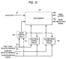
- a signal input to a video input 101 is written via a write port of a field memory 102 via control of a write control circuit 103.
- the signal written to the field memory 102 is delayed by a single field, read from a first read port of the field memory 102 via control of a first read control circuit 104, and read from a second read port of the field memory via control of a second read control circuit 105.
- the first read control circuit 104 performs control to read a signal in an area from an address given by a read start relative address 107 to an address given by a read end relative address 108.
- the signal read from the first port of the field memory 102 is output from a video output 106 and electronically enlarged by an interpolation circuit (not shown).
- a second read control circuit 105 reads the signal in the entire signal write area.
- a signal read from the second port of the field memory 102 is used as a noise reduction signal 109 by a cyclic noise reduction circuit (not shown).
- the write control circuit 103 performs control to start writing from the address next to the address given by a read end relative address 108.
- a write address does not pass by a first read address. The above operation is synchronized by a synchronization signal 110.
- a plurality of features such as the electronic enlargement feature and cyclic noise reduction feature can be realized simultaneously by controlling a field memory in the form of a ring via use of a three-port field memory having one write port and two read ports.
- the invention solves such a problem.
- the invention aims at reading a normal video signal by prevention a write address front passing by a read address even in a case where a combination of the CCD storage sensitivity enhancement feature, the cyclic noise reduction feature and the electronic enlargement feature is used, by using a three-port field memory having one write port and two read ports.
- imaging apparatus having a video memory function comprises: a video memory having a plurality of read ports and a capacity of storing images in two fields or more, wherein CCD storage sensitivity enhancement means is connected to a write port; a write control circuit for storing a single-field image in each memory area provided by dividing the storage space of the video memory into a plurality of sub-spaces; a plurality of read control sections for reading a single-field image stored in each memory area; and memory control means for reading an image from the video memory by a delay amount corresponding to the timing of a synchronization signal from the CCD storage sensitivity enhancement means.
- This configuration allows adjustment of the delay amount and prevents an image write address from passing by an image read address so that image data given CCD storage sensitivity enhancement is processed normally.
- vertical inversion read means connected to the read ports. This configuration prevents an image write address from passing by an image read address thus enabling a normal vertical inversion processing.
- noise reduction means connected to the read ports. This configuration prevents an image write address from passing by an image read address thus enabling a normal noise reduction processing.
- the first aspect of the invention is imaging apparatus having a video memory function comprising: a video memory having a plurality of read ports and a capacity of storing images in two fields or more, wherein CCD storage sensitivity enhancement means is connected to a write port; a write control circuit for storing a single-field image in each memory area provided by dividing the storage space of the image memory into a plurality of sub-spaces; a plurality of read control sections for reading a single-field image stored in each memory area; and memory control means for reading an image from the image memory by a delay amount corresponding to the timing of a synchronization signal from the CCD storage sensitivity enhancement means.
- This aspect has an effect of reading images given CCD sensitivity enhancement in proper time order.
- the second aspect of the invention is imaging apparatus according to the first aspect of the invention, equipped with electronic enlargement means connected to the read ports. This aspect has an effect of performing enlargement without disturbing the time order.
- the third aspect of the invention is imaging apparatus according to the first aspect of the invention, equipped with vertical inversion read means connected to the read ports. This aspect has an effect of performing vertical inversion without disturbing the time order.
- the fourth aspect of the invention is imaging apparatus according to the first aspect of the invention, equipped with noise reduction means connected to the read ports. This aspect has an effect of performing noise reduction without disturbing the time order.
- the fifth aspect of the invention is imaging apparatus according to any one of the first aspect through the fourth aspect, equipped with means for automatically determining an input image field based on a horizontal synchronization signal and a vertical synchronization signal and means for setting a memory area where image data is to be written depending on a sensitivity enhancement control signal from a CPU.
- This aspect has an effect of obtaining and setting a proper memory area where image data is to be written from a horizontal synchronization signal and a vertical synchronization signal.
- the sixth aspect of the invention is imaging apparatus according to the fifth aspect, equipped with a circuit for generating a vertical color order identification signal corresponding to a read field and a read address according to an electronic enlargement control signal and a CCD storage sensitivity enhancement mode control signal, wherein the vertical color order identification signal can be reset to an initial value for each field via the CPU.
- This aspect has an effect of generating a proper vertical color order identification signal.
- a first embodiment of the invention is imaging apparatus having a video memory function which stores two-field image data given CCD storage enhancement in a three-port memory, reads the data with an appropriate delay, then performs electronic enlargement, vertical inversion and noise reduction.
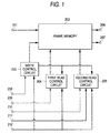
- Fig. 1 is a functional block diagram of imaging apparatus having a video memory function according to the first embodiment of the invention.
- an input terminal 201 is a terminal for inputting a video input signal.
- a frame memory 202 is a three-port memory having a capacity of storing images in two fields or more.
- a write control circuit 203 is a circuit for controlling data read from a first read port of the frame memory 202.
- a first read control circuit 204 is a circuit for controlling data read from a first read port of the frame memory 202.
- a second read control circuit 205 is a circuit for controlling data read from a second read port of the frame memory 202.
- An output terminal 206 is a terminal for outputting a video output signal read from the frame memory 202 according to control of the first read control circuit 204.
- An output terminal 207 is a terminal for outputting a video output signal read from the frame memory 202 according to control of the second read control circuit 205.
- a write area control terminal 208 is a terminal for controlling to which area of the frame memory 202 the write control circuit 203 will write an image.
- a first read area control terminal 209 is a terminal for controlling from which area of the frame memory 202 the first read control circuit 204 will read an image.
- a second read area control terminal 210 is a terminal for controlling from which area of the frame memory 202 the second read control circuit 205 will read an image.
- a read address setting terminal 211 is a terminal for determining from which address the second read control circuit 205 will read an image stored in the frame memory 202.
- a synchronization signal input terminal 212 is a terminal for inputting a synchronization signal.
- the write control circuit 203, the first read control circuit 204 and the second read control circuit 205 operate, according to the synchronization signal, in synchronization with a video signal input to the input terminal 201 and a video signal processing circuit connected externally to the output terminals 206 and 207.
- a video input to the input terminal 201 is written to an area of the frame memory 202 specified by the write area control terminal 208, by using the write address of the frame memory 202 and a write control signal generated by the write control circuit synchronized by the synchronization signal input to the synchronization signal input terminal 212.
- the first read control circuit 204 is synchronized by the synchronization signal input to the synchronization signal input terminal 212, generates a first read address of the frame memory 202 and a first read control signal, reads an image from an area of the frame memory 202 specified by the first read area control terminal 209, then outputs the image from the output terminal 206.
- the second read control circuit 205 is synchronized by the synchronization signal input to the synchronization signal input terminal 212, generates a second read address of the frame memory 202 and a second read control signal, reads an image from an area of the frame memory 202 specified by the second read area control terminal 210, then outputs the image from the output terminal 207.
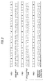
- Fig. 2 shows the relationship between a video signal input to the input terminal 201, a video signal output from the output terminal 206, 207, and fields in each signal.
- the relationship shown in Fig. 2 is a relationship in the normal mode.
- fields indicate each field for each video signal.
- a video signal input to the input terminal 201 is indicated as a video input.
- a video signal output from the output terminal 206 is indicated as a cyclic output.
- a video signal output from the output terminal 207 is indicated as a sensitivity enhancement output.
- the cyclic output signal is output with one frame delay after the video input.
- the sensitivity enhancement signal is output with one field delay after the video input.
- a video signal input to the input terminal 201 is indicated as a video input.
- a video signal output from the output terminal 206 is indicated as a cyclic output.
- a video signal output from the output terminal 207 is indicated as a sensitivity enhancement output.
- the area for storing images in Field A is indicated as Bank 0
- the area for storing images in Field B is indicated as Bank 1, which is indicated as a write bank in Fig. 3.
- a write bank signal is input alternately as 0, 1, 0, 1, 0,... from the write area control terminal 208, input alternately as 0, 1, 0, 1, 0,... from the first read area control terminal 209, and input alternately as 0, 1, 0, 1, 0,... from the second read area control terminal 210.
- the system enters the CCD storage sensitivity doubling operation in the fourth field.
- an image from Field B is inhibited and CCD charge storage is doubled for an image in Field A. That is, input of images (n+1), (n+3), (n+5), (n+7), and (n+8) is inhibited.
- the write control circuit 203 inhibits data write to the frame memory 202 during a period when no images are input.
- images in Bank 0 are updated but images in Bank 1 are not.
- images in Field A of a cyclic output are sequentially updated while images in Field B of the output remains as they were before the CCD storage sensitivity doubling mode started.
- images in Field A of a sensitivity enhancement output are sequentially updated while images in Field B of the output remains as they were before the CCD storage sensitivity doubling mode started.
- a video signal input to the input terminal 201 is indicated as a video input.
- a video signal output from the output terminal 206 is indicated as a cyclic output.
- a video signal output from the output terminal 207 is indicated as a sensitivity enhancement output.
- the area for storing images in Field A is indicated as Bank 0
- the area for storing images in Field B is indicated as Bank 1, which is indicated as a write bank in Fig. 4.
- a write bank is inverted from the write area control terminal 208 each time a video input is received.
- a control signal is input to the first read area control terminal 209 so that the newest image of all the images written before one frame stored in the frame memory is read.
- a control signal is input to the second read area control terminal 210 so that the newest image of all the images written before one frame stored in the frame memory is read.
- the CCD storage sensitivity doubling mode bank are switched from field to field and images are stored in a period when images are input.
- the signal at the first read area control terminal 209 is controlled as shown in Fig. 4, the newest image in both Field A and Field B can be output as cyclic output. Note that, because the same image is output for Field A and Field B, a shift of 0.5 lines must be corrected.
- the signal at the second read area control terminal 210 is controlled as shown in Fig. 4
- the newest image in both Field A and Field B can be output as cyclic output. Note that, because the same image is output for Field A and Field B, a shift in 0.5 lines must be corrected. In this way, normal data read in the CCD storage sensitivity doubling mode is realized.
- a video signal input to the input terminal 201 is indicated as a video input.
- a video signal output from the output terminal 206 is omitted in Fig. 5.
- a video signal output from the output terminal 207 is indicated as a sensitivity enhancement output.
- the area for storing images in Field A is indicated as Bank 0
- the area for storing images in Field B is indicated as Bank 1, which is indicated as a write bank in Fig. 5.
- a write bank is inverted from the write area control terminal 208 each time a video input is received.
- a control signal is input to the first read area control terminal 209 so that the newest image of all the images written before one frame stored in the frame memory is read. Also, a control signal is input to the second read area control terminal 210 so that the newest image of all the images written before one frame stored in the frame memory is read.
- the system enters the CCD storage sensitivity doubling operation in the fourth field.
- input of images from Field B is inhibited and CCD charge storage is doubled for an image in Field A. That is, input of images (n+1), (n+3), (n+5), (n+7), and (n+8) is inhibited.
- the write control circuit 203 inhibits data write to the frame memory 202 during a period when no images are input.
- a write address in the frame memory generated by the write control circuit 203 is indicated as a write address which increases monotonically.
- a read address in the frame memory generated by the second read control circuit 205 is indicated as a read address. The read address decreases monotonically in the case of vertical inversion read processing.
- a signal at the write area control terminal 208, a signal at the first read area control terminal 209 and a signal at the second read area control terminal 210 are used in order that a write bank and read bank for the frame memory always differ from each other. Accordingly, the newest image can be output from among sensitivity enhancement output signals in vertical inversion read processing. This prevents an unacceptable image due to inversion of a write address and a read address.
- a video signal input to the input terminal 201 is indicated as a video input.
- a video signal output from the output terminal 206 is omitted in Fig. 6.
- a video signal output from the output terminal 207 is indicated as a sensitivity enhancement output.
- the area for storing images in Field A is indicated as Bank 0
- the area for storing images in Field B is indicated as Bank 1, which is indicated as a write bank in Fig. 6.
- a write bank is inverted from the write area control terminal 208 each time a video input is received.
- a control signal is input to the first read area control terminal 209 so that the newest image of all the images written before one frame stored in the frame memory is read.
- a control signal is input to the second read area control terminal 210 so that the newest image of all the images written before one frame stored in the frame memory is read.
- the system enters the CCD storage sensitivity doubling operation in the fourth field. In this operation, an image from Field B is inhibited and CCD charge storage is doubled for an image in Field A. That is, input of images (n+1), (n+3), (n+5), (n+7), and (n+8) is inhibited.
- the write control circuit 203 inhibits data write to the frame memory 202 during a period when no images are input.
- a write address in the frame memory generated by the write control circuit 203 is indicated as a write address which increases monotonically.
- a read address in the frame memory generated by the second read control circuit 205 is indicated as a read address. The read address starts from any address and increases monotonically. In a conventional scheme, read processing and write processing occur simultaneously and the read address which is monotonically increasing from any address may pass by the write address increasing monotonically from zero (0). In happened that image data read around the address matching point was written at different times, thus generating an unacceptable image.
- a signal at the write area control terminal 208, a signal at the first read area control terminal 209 and a signal at the second read area control terminal 210 are used in order that a write bank and read bank for the frame memory always differ from each other. Accordingly, a read address never passes by a read address in electronic enlargement. The newest image is always output from among the sensitivity enhancement output signals. This prevents an unacceptable image from being generated.
- imaging apparatus having a video memory function has a configuration wherein two-field image data given CCD storage enhancement is stored in a three-port memory, and the data is read with any delay for electronic enlargement, vertical inversion and noise reduction. This allows more than one type of image processing to be made in proper time order.
- a second embodiment of the invention is imaging apparatus having a video memory function which automatically determines an input image field based on a horizontal synchronization signal and a vertical synchronization signal and sets a memory area where image data is to be written depending on a sensitivity enhancement control signal from a CPU.
- Fig. 7 is a functional block diagram of imaging apparatus having a video memory function according to the second embodiment of the invention.
- imaging apparatus having a video memory function 701 is apparatus shown in the first embodiment.
- An area control circuit 702 is a circuit which automatically generates each of area control signals used to control the write control circuit 203, the first read control circuit 204 and the second read control circuit 205.
- An input terminal 703 is a terminal for inputting the horizontal synchronization signal.
- An input terminal 704 is a terminal for inputting the vertical synchronization signal.
- An input terminal 705 is a terminal for inputting the CCD storage sensitivity enhancement control signal from the CPU.
- An input terminal 706 is a terminal for inputting the video input signal.
- a read address setting terminal 707 is a terminal for inputting a signal for determining from which address the second read control circuit 205 should read the image stored in the frame memory 202.
- An output terminal 708 is a terminal for outputting a video output signal read from the frame memory 202 according to the control of the first read control circuit 204.
- An output terminal 709 is a terminal for outputting a video output signal read from the frame memory 202 according to the control of the second read control circuit 205.
- a first area control signal 710 is a signal generated by the area control circuit 702 to control the write control circuit 203.
- a second area control signal 711 is a signal generated by the area control circuit 702 to control the first read control circuit 204.
- a third area control signal 712 is a signal generated by the area control circuit 702 to control the second read control circuit 205.
- a video signal input to the input terminal 706 is input always in synchronization with the horizontal synchronization signal input to the input terminal 703 and the vertical synchronization signal input to the input terminal 704.
- a CCD storage sensitivity enhancement control signal reports to the area control circuit 702 whether the video signal input to the input terminal 706 is a normal video signal or a video signal in the CCD storage sensitivity enhancement mode.
- the area control circuit 702 provides the imaging apparatus having a video memory function 701 with the first area control signal 710, the second area control signal 711, and the third area control signal 712.
- the imaging apparatus having a video memory function according to the second embodiment of the invention can thus automatically determine the bank used for storing image data in the frame memory 202, only via a CCD storage sensitivity control signal.
- a video signal input to the input terminal 706 is indicated as a video input.
- a CCD storage sensitivity enhancement control signal input to the input terminal 705 is indicated as a sensitivity enhancement control.
- the first area control signal is indicated as the area control signal 1.
- the second area control signal is indicated as the area control signal 2.
- the third area control signal is indicated as the area control signal 3.
- a video signal output from the output terminal 708 is indicated as a cyclic output.
- a video signal output from the output terminal 709 is indicated as a sensitivity enhancement output.
- the write control circuit 203 writes an image to Bank 0 of the frame memory 202, and in case the area control signal 1 is '1', to Bank 1.
- the sensitivity enhancement control is set to 0 (normal mode)
- control is made so that the area control signal 1 is '0' when images are input from Field A, and '0' when images are input from Field B.
- the sensitivity enhancement control is set to 2
- input of images from Field B is inhibited and only images from Field A are input.
- the area control signal 1 is generated so that banks are sequentially switched from field to field containing video signals to be input.
- the write control circuit 203 writes an image to Bank 0 of the frame memory 202, and in case the area control signal 1 is '1', to Bank 1.
- the sensitivity enhancement control is set to 0 (normal mode)
- control is made so that the area control signal 1 is '0' when images are input from Field A, and '0' when images are input from Field B.
- the sensitivity enhancement control is set to 2
- images in either bank of the frame memory 202 is updated once in two fields.
- the area control signal 2 is generated so that banks are sequentially switched to read images in the frame memory 202 while keeping an cyclic output delayed at least one frame from a video input.
- the write control circuit 203 writes an image to Bank 0 of the frame memory 202, and in case the area control signal 1 is '1', to Bank 1.
- the sensitivity enhancement control is set to 0 (normal mode)
- control is made so that the area control signal 1 is '0' when images are input from Field A, and '0' when images are input from Field B.
- the sensitivity enhancement control is set to 2
- images in either bank of the frame memory 202 is updated once in two fields.
- the area control signal 2 is generated so that banks are sequentially switched to read images in the frame memory 202 while keeping a sensitivity enhancement output delayed at least one field from a video input.
- imaging apparatus having a video memory function is configured to automatically determine an input image field based on a horizontal synchronization signal and a vertical synchronization signal and to set a memory area where image data is to be written depending on a sensitivity enhancement control signal from a CPU. This allows the bank used for storing image data in the frame memory 202 to be determined, only via a CCD storage sensitivity control signal.
- a third embodiment of the invention is imaging apparatus which generates a vertical color order identification signal corresponding to a read field and a read address according to an electronic enlargement control signal and a CCD storage sensitivity enhancement mode control signal, wherein the vertical color order identification signal can be reset to an initial value for each field via the CPU.
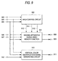
- Fig. 9 is a functional block diagram of imaging apparatus having a video memory function according to the third embodiment of the invention.
- imaging apparatus having a video memory function 901 is a circuit shown in the second embodiment.
- An input terminal 903 is a terminal for inputting the horizontal synchronization signal.
- An input terminal 904 is a terminal for inputting the vertical synchronization signal.
- An input terminal 905 is a terminal for inputting the CCD storage sensitivity enhancement control signal from the CPU.
- An input terminal 906 is a terminal for inputting the video input signal.
- a read address setting terminal 907 is a terminal for setting a read address for determining from which address the second read control circuit 205 should read the image stored in the frame memory 202.
- An output terminal 908 is a terminal for outputting a video output signal read from the frame memory 202 according to the control of the first read control circuit 204.
- An output terminal 909 is a terminal for outputting a video output signal read from the frame memory 202 according to the control of the second read control circuit 205.
- a vertical color identification signal generator circuit 910 is a vertical color identification signal generator circuit for automatically generating a vertical color identification signal by using the horizontal synchronization signal input to the input terminal 903, the vertical synchronization signal input to the input terminal 904, and the CCD storage sensitivity enhancement control signal input to the input terminal 905.
- An input terminal 912 is a terminal for inputting an initial value setting control signal for setting an initial value of the vertical color identification signal generated by the vertical color identification signal generator circuit 910.
- An output terminal 911 is a terminal for outputting a vertical color identification signal as an output signal from the vertical color identification signal generator circuit.
- the area control circuit 902 specifies a write bank and a read bank of the frame memory 202 for the write control circuit 203, the first read control circuit 204 and the second read control circuit 205 of the imaging apparatus having a video memory function 901.
- the bank of the frame memory to which the write control circuit 203 wrote video data that is, bank 0 or bank 1, and the corresponding field which retains such data, Field A or Field B, are stored in the register.
- the vertical color identification signal generator circuit 910 can automatically generate a vertical color identification signal.
- the imaging apparatus having a video memory function can generate a vertical color identification signal corresponding to a video output signal only via a CCD storage sensitivity control signal from the CPU.
- a video signal input to the input terminal 906 is indicated as a video input.
- a CCD storage sensitivity enhancement control signal input to the input terminal 905 is indicated as a sensitivity enhancement control.
- the first area control signal is indicated as the area control signal 1.
- the second area control signal is indicated as the area control signal 2.
- the third area control signal is indicated as the area control signal 3.
- a video signal output from the output terminal 908 is indicated as a cyclic output.
- a video signal output from the output terminal 909 is indicated as a sensitivity enhancement output.
- a vertical color identification signal is shown at the bottom section.
- a vertical color identification signal is a signal for identifying the layout of video signals per line in synchronization with a horizontal synchronization signal. The phase is identical between the signals in video input for Field A. The same is true for Field B.
- the vertical color identification signal generator circuit 910 can automatically generate a vertical color identification signal from a field of the video data read from the frame memory 202. Once a decision is made as to whether the read start line is even or odd before vertical inversion or electronic enlargement, a vertical color identification signal can be automatically generated.
- a vertical color identification signal control circuit 1101 an identification signal generator for Field A 1102; an identification signal generator for Field B 1103; a selector 1104 for switching between an output of the identification signal generator for Field A 1102 and an output of the identification signal generator for Field B 1103; an input terminal 1105 for inputting a vertical synchronization signal; an input terminal 1105 for inputting a vertical synchronization signal; an input terminal 1106 for inputting a horizontal synchronization signal; a CCD sensitivity enhancement signal from the CPU 1107; an initial value setting control signal 1108 for a vertical color identification signal for Field A and a vertical color identification signal for Field B; a phase correction circuit 1109 for applying phase correction in case the phase of a vertical color identification signal is to be adjusted via magnitude of sensitivity enhancement; and a vertical color identification signal 1110 which was selected via the selector 1104 and passed through the phase correction circuit 1109.
- the vertical color identification signal control circuit 1101 determines the initial value of the vertical color identification signal which conforms to the CCD specifications, based on the initial value setting control signal from the CPU and sets the initial value to the identification signal generator for Field A 1102 and the identification signal generator for Field B 1103. In case the vide signal input is made in the normal mode, the identification signal generator for Field A 1102 and the identification signal generator for Field B 1103 repeat the sequence of reset and inversion in specified timing, in synchronization with a horizontal synchronization signal.
- the vertical color identification signal control circuit 1101 determines the field of the video signal output from the sensitivity enhancement output based on the phase relationship between the horizontal synchronization signal and the vertical synchronization signal.
- the vertical color identification signal corresponding to the field of the video signal output from the sensitivity enhancement output is output with the selector switched as required.
- the selector 1104 is switched after determining the field of the video signal output from the sensitivity enhancement output depending on the multiple for sensitivity enhancement in the CCD storage sensitivity enhancement operation.
- a phase shift of 0.5 lines in image data caused by a certain magnitude of sensitivity enhancement must be corrected by using the phase correction circuit 1109.
- imaging apparatus having a video memory function is configured to generate a vertical color order identification signal corresponding to a read field and a read address according to an electronic enlargement control signal and a CCD storage sensitivity enhancement mode control signal, wherein the vertical color order identification signal can be reset to an initial value for each field via the CPU.
- This allows a vertical color identification signal corresponding to a video output signal to be automatically output from an output terminal only via a CCD storage sensitivity control signal from the CPU.
- imaging apparatus having a video memory function comprises: a video memory having a plurality of read ports and a capacity of storing images in two fields or more, wherein CCD storage sensitivity enhancement means is connected to a write port; a write control circuit for storing a single-field image in each memory area provided by dividing the storage space of the video memory into a plurality of sub-spaces; a plurality of read control sections for reading a single-field image stored in each memory area; memory control means for reading an image from the video memory by a delay amount corresponding to the timing of a synchronization signal from the CCD storage sensitivity enhancement means; electronic enlargement means; vertical inversion read means; and noise reduction means.
- This configuration provides an advantage that a combination of the cyclic noise reduction feature, CCD sensitivity enhancement feature, electronic enlargement feature and vertical inversion processing can be realized without inversion of the time order of images.
- This configuration has an advantage that a bank used for storing images in the frame memory can be automatically determined only via a CCD storage sensitivity enhancement control signal from the CPU.
Landscapes
- Engineering & Computer Science (AREA)
- Multimedia (AREA)
- Signal Processing (AREA)
- Studio Devices (AREA)
- Television Signal Processing For Recording (AREA)
- Picture Signal Circuits (AREA)
- Studio Circuits (AREA)
- Transforming Light Signals Into Electric Signals (AREA)
Abstract
Description
Claims (6)
- Imaging apparatus having a video memory function, comprises:a video memory having a plurality of read ports and a capacity of storing images in two fields or more wherein CCD storage sensitivity enhancement means is connected to a write port;a write control circuit for storing a single-field image in each memory area provided by dividing the storage space of said video memory into a plurality of sub-spaces;a plurality of read control sections for reading a single-field image stored in each of said memory areas; andmemory control means for reading an image from said video memory by a delay amount corresponding to the timing of a synchronization signal from said CCD storage sensitivity enhancement means.
- Imaging apparatus having a video memory function according to Claim 1, further comprising electronic enlargement means connected to said read ports.
- Imaging apparatus having video memory function according to Claim 1, further comprising vertical inversion read means connected to said read ports.
- Imaging apparatus having a video memory function according to Claim 1, further comprising noise reduction means connected to said read ports.
- Imaging apparatus having a video memory function according to any one of the preceding claims, further comprising means for automatically determining an input image field based on a horizontal synchronization signal and a vertical synchronization signal, a CPU for outputting a sensitivity enhancement signal, and means for setting a memory area where image data is to be written depending on said sensitivity enhancement control signal.
- Imaging apparatus having a video memory function according to Claim 5, further comprising a circuit for generating a vertical color order identification signal corresponding to a read field and a read address according to an electronic enlargement control signal from said electronic enlargement means and a CCD storage sensitivity enhancement mode control signal from said vertical inversion read means and that said apparatus has means for resetting said vertical color order identification signal to an initial value for each field via the CPU.
Applications Claiming Priority (2)
| Application Number | Priority Date | Filing Date | Title |
|---|---|---|---|
| JP11168692A JP2000358193A (en) | 1999-06-15 | 1999-06-15 | Video device with image memory function |
| JP16869299 | 1999-06-15 |
Publications (2)
| Publication Number | Publication Date |
|---|---|
| EP1061735A2 true EP1061735A2 (en) | 2000-12-20 |
| EP1061735A3 EP1061735A3 (en) | 2003-12-17 |
Family
ID=15872703
Family Applications (1)
| Application Number | Title | Priority Date | Filing Date |
|---|---|---|---|
| EP00112713A Withdrawn EP1061735A3 (en) | 1999-06-15 | 2000-06-15 | Imaging apparatus having a multi port memory |
Country Status (8)
| Country | Link |
|---|---|
| US (1) | US6744476B1 (en) |
| EP (1) | EP1061735A3 (en) |
| JP (1) | JP2000358193A (en) |
| CN (1) | CN1277518A (en) |
| AU (1) | AU771919B2 (en) |
| CA (1) | CA2311063A1 (en) |
| MX (1) | MXPA00005911A (en) |
| NZ (1) | NZ505104A (en) |
Families Citing this family (3)
| Publication number | Priority date | Publication date | Assignee | Title |
|---|---|---|---|---|
| FR2842978B1 (en) * | 2002-07-26 | 2005-03-04 | Thomson Licensing Sa | DEVICE AND METHOD FOR DELAYED READING OF DIGITAL VIDEO DATA |
| JP3991064B2 (en) * | 2004-10-14 | 2007-10-17 | 松下電器産業株式会社 | Video signal processing device |
| CN114281295B (en) * | 2020-09-18 | 2024-03-15 | 西安诺瓦星云科技股份有限公司 | Image processing method and device and LED display screen system |
Family Cites Families (16)
| Publication number | Priority date | Publication date | Assignee | Title |
|---|---|---|---|---|
| US4240101A (en) * | 1976-10-14 | 1980-12-16 | Micro Consultants, Limited | Television standards conversion |
| EP0249985B1 (en) * | 1986-06-20 | 1993-09-08 | Sony Corporation | Video memory |
| KR910006460B1 (en) * | 1988-03-08 | 1991-08-26 | 삼성전자 주식회사 | Flickering Reduction Device and Method for Frame Still Image in Digital Video Equipment |
| US5418907A (en) * | 1991-09-12 | 1995-05-23 | Sony Corporation | Multi-port memory and digital interpolation apparatus |
| US5315388A (en) * | 1991-11-19 | 1994-05-24 | General Instrument Corporation | Multiple serial access memory for use in feedback systems such as motion compensated television |
| US5345264A (en) * | 1992-02-27 | 1994-09-06 | Sanyo Electric Co., Ltd. | Video signal processing circuit for a video camera using a luminance signal |
| JPH0773342B2 (en) | 1992-03-02 | 1995-08-02 | 三洋電機株式会社 | Video signal processing circuit |
| WO1994003015A1 (en) * | 1992-07-22 | 1994-02-03 | Matsushita Electric Industrial Co., Ltd. | Imaging device with horizontal line interpolation function |
| JP2667580B2 (en) * | 1993-12-27 | 1997-10-27 | 株式会社エース電研 | Image display game apparatus and image display control method thereof |
| US5459510A (en) * | 1994-07-08 | 1995-10-17 | Panasonic Technologies, Inc. | CCD imager with modified scanning circuitry for increasing vertical field/frame transfer time |
| JP3840671B2 (en) * | 1995-03-24 | 2006-11-01 | ソニー株式会社 | Imaging device |
| JP2956527B2 (en) | 1995-04-28 | 1999-10-04 | 松下電器産業株式会社 | Video device with image memory function |
| JP3384659B2 (en) * | 1995-10-16 | 2003-03-10 | 三洋電機株式会社 | Reduced video signal processing circuit |
| KR970064171A (en) * | 1996-02-28 | 1997-09-12 | 이대원 | Image reversing device |
| EP0825781B1 (en) * | 1996-08-22 | 2004-10-27 | Matsushita Electric Industrial Co., Ltd. | Image processor |
| JP3717648B2 (en) * | 1997-11-07 | 2005-11-16 | 株式会社エルモ社 | Method for creating enlarged image signal using field memory |
-
1999
- 1999-06-15 JP JP11168692A patent/JP2000358193A/en active Pending
-
2000
- 2000-06-07 US US09/589,240 patent/US6744476B1/en not_active Expired - Fee Related
- 2000-06-08 CA CA002311063A patent/CA2311063A1/en not_active Abandoned
- 2000-06-12 NZ NZ505104A patent/NZ505104A/en unknown
- 2000-06-14 AU AU40835/00A patent/AU771919B2/en not_active Ceased
- 2000-06-14 CN CN00118334.6A patent/CN1277518A/en active Pending
- 2000-06-15 MX MXPA00005911A patent/MXPA00005911A/en active IP Right Grant
- 2000-06-15 EP EP00112713A patent/EP1061735A3/en not_active Withdrawn
Also Published As
| Publication number | Publication date |
|---|---|
| MXPA00005911A (en) | 2002-06-04 |
| NZ505104A (en) | 2001-08-31 |
| EP1061735A3 (en) | 2003-12-17 |
| AU771919B2 (en) | 2004-04-08 |
| US6744476B1 (en) | 2004-06-01 |
| AU4083500A (en) | 2000-12-21 |
| JP2000358193A (en) | 2000-12-26 |
| CA2311063A1 (en) | 2000-12-15 |
| CN1277518A (en) | 2000-12-20 |
Similar Documents
| Publication | Publication Date | Title |
|---|---|---|
| JP5008826B2 (en) | High-definition deinterlacing / frame doubling circuit and method thereof | |
| JPS63207284A (en) | Picture-in-picture video signal generator | |
| JP3188135B2 (en) | Video signal processing circuit | |
| US6067120A (en) | Video signal conversion device for reducing flicker in non-interlaced to interlaced signal conversion | |
| US6747656B2 (en) | Image processing apparatus and method of the same, and display apparatus using the image processing apparatus | |
| US6744476B1 (en) | Imaging apparatus having video memory function | |
| JPH0622197A (en) | Picture processing unit | |
| US5856849A (en) | Digital processing of video signals for performing aspect ratio conversion | |
| EP0740464B1 (en) | Video apparatus with a single multi-port field memory | |
| JPS5967788A (en) | Still image generator for television receivers | |
| US6891569B1 (en) | Wide angle image pickup apparatus | |
| US6111615A (en) | Address generating and mapping device of video capture system | |
| JPH05308544A (en) | Video signal processor | |
| JP2622622B2 (en) | Scan line number conversion control method | |
| KR100331797B1 (en) | Apparatus for memory controlling of digital TV | |
| JP2002101376A (en) | Line memory | |
| US6104440A (en) | Prompter eliminating phase shift in sub-carriers | |
| JP2897521B2 (en) | Semiconductor memory | |
| US7061543B1 (en) | Method and circuit for image-in-image overlay | |
| KR0132262Y1 (en) | Video horizontal interpolation circuit | |
| CN118898956A (en) | Image processing circuit and image processing method | |
| JPH05207425A (en) | Semiconductor memory | |
| JP2000295629A (en) | Image signal processing circuit | |
| JPH04299685A (en) | image processing circuit | |
| JPH0638643B2 (en) | Image memory address correction circuit |
Legal Events
| Date | Code | Title | Description |
|---|---|---|---|
| PUAI | Public reference made under article 153(3) epc to a published international application that has entered the european phase |
Free format text: ORIGINAL CODE: 0009012 |
|
| AK | Designated contracting states |
Kind code of ref document: A2 Designated state(s): AT BE CH CY DE DK ES FI FR GB GR IE IT LI LU MC NL PT SE |
|
| AX | Request for extension of the european patent |
Free format text: AL;LT;LV;MK;RO;SI |
|
| PUAL | Search report despatched |
Free format text: ORIGINAL CODE: 0009013 |
|
| AK | Designated contracting states |
Kind code of ref document: A3 Designated state(s): AT BE CH CY DE DK ES FI FR GB GR IE IT LI LU MC NL PT SE |
|
| AX | Request for extension of the european patent |
Extension state: AL LT LV MK RO SI |
|
| 17P | Request for examination filed |
Effective date: 20040217 |
|
| AKX | Designation fees paid |
Designated state(s): DE FR GB |
|
| 17Q | First examination report despatched |
Effective date: 20061018 |
|
| RAP1 | Party data changed (applicant data changed or rights of an application transferred) |
Owner name: PANASONIC CORPORATION |
|
| STAA | Information on the status of an ep patent application or granted ep patent |
Free format text: STATUS: THE APPLICATION IS DEEMED TO BE WITHDRAWN |
|
| 18D | Application deemed to be withdrawn |
Effective date: 20090106 |