EP1061577A2 - High frequency multi-layered circuit component - Google Patents
High frequency multi-layered circuit component Download PDFInfo
- Publication number
- EP1061577A2 EP1061577A2 EP00112296A EP00112296A EP1061577A2 EP 1061577 A2 EP1061577 A2 EP 1061577A2 EP 00112296 A EP00112296 A EP 00112296A EP 00112296 A EP00112296 A EP 00112296A EP 1061577 A2 EP1061577 A2 EP 1061577A2
- Authority
- EP
- European Patent Office
- Prior art keywords
- high frequency
- power supply
- supply line
- layers
- circuit component
- Prior art date
- Legal status (The legal status is an assumption and is not a legal conclusion. Google has not performed a legal analysis and makes no representation as to the accuracy of the status listed.)
- Granted
Links
Images


Classifications
-
- H—ELECTRICITY
- H03—ELECTRONIC CIRCUITRY
- H03H—IMPEDANCE NETWORKS, e.g. RESONANT CIRCUITS; RESONATORS
- H03H7/00—Multiple-port networks comprising only passive electrical elements as network components
- H03H7/01—Frequency selective two-port networks
- H03H7/0115—Frequency selective two-port networks comprising only inductors and capacitors
-
- H—ELECTRICITY
- H10—SEMICONDUCTOR DEVICES; ELECTRIC SOLID-STATE DEVICES NOT OTHERWISE PROVIDED FOR
- H10W—GENERIC PACKAGES, INTERCONNECTIONS, CONNECTORS OR OTHER CONSTRUCTIONAL DETAILS OF DEVICES COVERED BY CLASS H10
- H10W44/00—Electrical arrangements for controlling or matching impedance
- H10W44/20—Electrical arrangements for controlling or matching impedance at high-frequency [HF] or radio frequency [RF]
-
- H—ELECTRICITY
- H10—SEMICONDUCTOR DEVICES; ELECTRIC SOLID-STATE DEVICES NOT OTHERWISE PROVIDED FOR
- H10W—GENERIC PACKAGES, INTERCONNECTIONS, CONNECTORS OR OTHER CONSTRUCTIONAL DETAILS OF DEVICES COVERED BY CLASS H10
- H10W44/00—Electrical arrangements for controlling or matching impedance
- H10W44/601—Capacitive arrangements
-
- H—ELECTRICITY
- H10—SEMICONDUCTOR DEVICES; ELECTRIC SOLID-STATE DEVICES NOT OTHERWISE PROVIDED FOR
- H10W—GENERIC PACKAGES, INTERCONNECTIONS, CONNECTORS OR OTHER CONSTRUCTIONAL DETAILS OF DEVICES COVERED BY CLASS H10
- H10W70/00—Package substrates; Interposers; Redistribution layers [RDL]
- H10W70/60—Insulating or insulated package substrates; Interposers; Redistribution layers
- H10W70/67—Insulating or insulated package substrates; Interposers; Redistribution layers characterised by their insulating layers or insulating parts
- H10W70/68—Shapes or dispositions thereof
-
- H—ELECTRICITY
- H03—ELECTRONIC CIRCUITRY
- H03H—IMPEDANCE NETWORKS, e.g. RESONANT CIRCUITS; RESONATORS
- H03H1/00—Constructional details of impedance networks whose electrical mode of operation is not specified or applicable to more than one type of network
- H03H2001/0021—Constructional details
- H03H2001/0085—Multilayer, e.g. LTCC, HTCC, green sheets
-
- H—ELECTRICITY
- H05—ELECTRIC TECHNIQUES NOT OTHERWISE PROVIDED FOR
- H05K—PRINTED CIRCUITS; CASINGS OR CONSTRUCTIONAL DETAILS OF ELECTRIC APPARATUS; MANUFACTURE OF ASSEMBLAGES OF ELECTRICAL COMPONENTS
- H05K1/00—Printed circuits
- H05K1/02—Details
- H05K1/0213—Electrical arrangements not otherwise provided for
- H05K1/0237—High frequency adaptations
-
- H—ELECTRICITY
- H05—ELECTRIC TECHNIQUES NOT OTHERWISE PROVIDED FOR
- H05K—PRINTED CIRCUITS; CASINGS OR CONSTRUCTIONAL DETAILS OF ELECTRIC APPARATUS; MANUFACTURE OF ASSEMBLAGES OF ELECTRICAL COMPONENTS
- H05K1/00—Printed circuits
- H05K1/02—Details
- H05K1/0296—Conductive pattern lay-out details not covered by sub groups H05K1/02 - H05K1/0295
- H05K1/0298—Multilayer circuits
-
- H—ELECTRICITY
- H05—ELECTRIC TECHNIQUES NOT OTHERWISE PROVIDED FOR
- H05K—PRINTED CIRCUITS; CASINGS OR CONSTRUCTIONAL DETAILS OF ELECTRIC APPARATUS; MANUFACTURE OF ASSEMBLAGES OF ELECTRICAL COMPONENTS
- H05K1/00—Printed circuits
- H05K1/16—Printed circuits incorporating printed electric components, e.g. printed resistors, capacitors or inductors
-
- H—ELECTRICITY
- H10—SEMICONDUCTOR DEVICES; ELECTRIC SOLID-STATE DEVICES NOT OTHERWISE PROVIDED FOR
- H10W—GENERIC PACKAGES, INTERCONNECTIONS, CONNECTORS OR OTHER CONSTRUCTIONAL DETAILS OF DEVICES COVERED BY CLASS H10
- H10W70/00—Package substrates; Interposers; Redistribution layers [RDL]
- H10W70/60—Insulating or insulated package substrates; Interposers; Redistribution layers
- H10W70/62—Insulating or insulated package substrates; Interposers; Redistribution layers characterised by their interconnections
- H10W70/63—Vias, e.g. via plugs
-
- H—ELECTRICITY
- H10—SEMICONDUCTOR DEVICES; ELECTRIC SOLID-STATE DEVICES NOT OTHERWISE PROVIDED FOR
- H10W—GENERIC PACKAGES, INTERCONNECTIONS, CONNECTORS OR OTHER CONSTRUCTIONAL DETAILS OF DEVICES COVERED BY CLASS H10
- H10W70/00—Package substrates; Interposers; Redistribution layers [RDL]
- H10W70/60—Insulating or insulated package substrates; Interposers; Redistribution layers
- H10W70/67—Insulating or insulated package substrates; Interposers; Redistribution layers characterised by their insulating layers or insulating parts
- H10W70/68—Shapes or dispositions thereof
- H10W70/682—Shapes or dispositions thereof comprising holes having chips therein
-
- H—ELECTRICITY
- H10—SEMICONDUCTOR DEVICES; ELECTRIC SOLID-STATE DEVICES NOT OTHERWISE PROVIDED FOR
- H10W—GENERIC PACKAGES, INTERCONNECTIONS, CONNECTORS OR OTHER CONSTRUCTIONAL DETAILS OF DEVICES COVERED BY CLASS H10
- H10W70/00—Package substrates; Interposers; Redistribution layers [RDL]
- H10W70/60—Insulating or insulated package substrates; Interposers; Redistribution layers
- H10W70/67—Insulating or insulated package substrates; Interposers; Redistribution layers characterised by their insulating layers or insulating parts
- H10W70/68—Shapes or dispositions thereof
- H10W70/685—Shapes or dispositions thereof comprising multiple insulating layers
Definitions
- the present invention relates to a high frequency multi-layered circuit component, more specifically, a high frequency multi-layered circuit component having active elements mounted thereon such as diodes, transistors, and ICs.
- a high frequency multi-layered circuit component is a composite component on which are mounted active elements such as diodes, transistors, and ICs as well as a plurality of passive circuit elements, for example, capacitors, inductors, and resistors distributed over a plurality of layers so that at least some of the plurality of circuit elements form a high frequency circuit.
- Such a high frequency multi-layered circuit component is provided with a power supply line for supplying direct-current power to the active elements, high frequency hot-lines included in the high frequency
- FIG. 6 schematically shows a typical example of the arrangement of the power supply line, high frequency hot-lines, and ground layers on a given cross-section of a conventional high frequency multi-layered circuit component.
- the power supply line 1 and high frequency hot-line 2 are mounted along the same layer to make it compact, while the ground layers 3 and 4 are disposed so as to sandwich the power supply line 1 and high frequency hot-line 2 between them.
- alternating-current noise components due to high frequency signals flowing through the high frequency hot-line 2 can interfere with the direct-current power that is supplied to the active elements (not shown) via the power supply line 1.
- the bias voltage of the active elements tends to fluctuate, destabilizing the operation of the active elements.
- the power supply line 1 is disposed comparatively close to the high frequency hot-line 2, alternating-current noise components the power supply line 1 tend to adversely affect the high frequency hot-line 2.
- An embodiment of the present invention provides a high frequency multi-layered circuit component that can solve the foregoing problems.
- a high frequency multi-layered circuit component comprises: a plurality of layers laminated to each other; an active element mounted on one of the plurality of layers; at least one passive circuit element formed within the plurality of layers; a high frequency circuit comprising at least a part of the at least one circuit element; a power supply line for supplying direct-current power to the active element disposed along one of the plurality of layers; high frequency hot-lines included in the high frequency circuit and disposed along other ones of the plurality of layers which are different from the one of the plurality of layers along which the power supply line is disposed; and a ground layer which generates capacitance with the power supply line and is disposed between the power supply line and the high frequency hot-lines.
- a pair of said ground layers may be provided so as to sandwich the power supply line between them.
- the pair of ground layers may be disposed with a narrow space between them so as to prevent high frequency signals from passing through the power supply line, by creating an impedance mismatch in the power supply line relative to the high frequency signals.
- the power supply line and the high frequency hot-lines from adversely affecting each other, since the power supply line for supplying direct-current power to the active element and the high frequency hot-lines included in the high frequency circuit are provided along mutually separated layers, and a ground layer is disposed between the power supply line and the high frequency hot-lines.
- the ground layer forms capacitance with the power supply line capacitance, thereby suppressing the alternating-current noise components, and preventing them from interfering with the direct-current power supplied through the power supply line.
- the two ground layers are disposed so as to sandwich the power supply line between them, the above-mentioned effect may be obtained even more securely.
- the pair of ground layers disposed to sandwich the power supply line between them it is possible to even further suppress the alternating-current noise components flowing through the power supply line by producing a mismatch in the power supply line relative to the high frequency signals by making the space between two ground layers narrow, so as to prevent high frequency signals from passing through the power supply line.
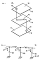
- FIG. 1 is a perspective view schematically illustrating a part of a high frequency multi-layered circuit component 11 in an embodiment of the present invention.
- FIG. 1 In FIG. 1 are shown three dielectric layers 12, 13, and 14 made of ceramics, for example, mutually separated, forming a part of the high frequency multi-layered circuit component 11. Additional layers, not shown in Fig. 1, are disposed above the dielectric layer 12 and below the dielectric layer 14. (In this disclosure, the terms “above” and “below” and the like are merely relative terms and the structures described herein need not be oriented as shown in the drawings.)
- the power supply line 15 is provided on the dielectric layer 13 positioned in the middle and the ground layers 16 and 17 are formed on the dielectric layers 12 and 14, respectively, so as to sandwich the power supply line between the layers.
- the ground layers 16 and 17 are on top sides of the layers 12 and 14, respectively, and the power supply line 15 is correspondingly on the top side of the layer 13.
- a plurality of passive circuit elements (not shown) for forming a high frequency circuit are located on at least respective ones of the additional layers above the dielectric layer 12 and below the dielectric layer 14.
- the high frequency hot-lines included in the high frequency circuit (not shown) are also provided along those additional upper or lower dielectric layers, not shown.
- Active elements such as diodes, transistors, and ICs are also mounted on the additional dielectric layers, other than the dielectric layers 12 to 14 shown in the drawing.
- An end of the power supply line 15 passes through a via-hole 18 to connect electrically to circuit elements or active elements located above the dielectric layer 12, while the other end of the power supply line 15 passes through a via-hole 19 to connect electrically to circuit elements or active elements located below the dielectric layer 14.
- a construction is formed in which a power supply line 15 and high frequency hot-lines are provided along mutually separated layers and a situation is realized in which the ground layers 16 and/or 17 are disposed between the power supply line 15 and high frequency hot-lines. Also, the ground layers 16 and 17 are located adjacent to the power supply line 15.
- FIG. 2 shows an equivalent circuit relating to the power supply line 15 in the arrangement shown in FIG. 1.
- FIG. 2 it is possible to form a capacitance between the power supply line 15 and the ground layers 16 and 17 by disposing the ground layers 16 and 17 adjacent to the power supply line 15 to form capacitance components 20 between the power supply line 15 and the ground layers 16 and 17. Accordingly, the alternating-current noise component on the power supply line can be reduced, since it can be diverted to the ground layers 16 and 17 through the capacitance component 20 as shown by arrows 21, so that the alternating-current noise component can be prevented from interfering with the direct-current power supplied through the power supply line 15.
- the additional way to suppress the alternating-current components is to form the power supply line 15 to have an impedance mismatch relative to the high frequency signals.
- the line width of the power supply line 15 is widened or the spaces between the line and the two ground layers are narrowed to have the impedance mismatch.
- an undesirable voltage drop in the power supply line 15 can be suppressed by providing the power supply line 15 with enough width to keep direct-current resistance in the power supply line 15 sufficiently low.
- the power supply line 15 should be more than 200 ⁇ m wide, for example.
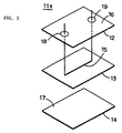
- FIG. 3 is a perspective view schematically illustrating a part of the high frequency multi-layered circuit component 11a in another embodiment of the present invention.
- FIG. 3 is a view corresponding to FIG. 1 and the elements corresponding to those shown in FIG. 1 are referred to by the same numerals to omit duplicated descriptions.
- the ends of the power supply line 15 pass through respective via-holes 18 and 19 to connect electrically to circuit elements and/or active elements located above the dielectric layer 12.
- the ground layer 17 may be omitted.
- the manner of routing of the power supply line within the high frequency multi-layered circuit component may be modified in various ways.
- FIG. 4 shows more specifically an example of a circuit that can be constructed in a composite component including the high frequency multi-layered circuit component of the present invention.
- the composite component shown in FIG. 4 forms, for example, a receiving circuit in a mobile telephone.
- a composite component 23 comprises low-noise amplifiers LNA1 and LNA2 for amplifying signals received by a receiving antenna, not shown, high pass filters HPF1 and HPF2 for passing only signals with higher than specified frequencies out of the received signals amplified by the low-noise amplifiers LNA1 and LNA2, and mixers M1 and M2 for processing the outputs from the high pass filters HPF1 and HPF2.
- the amplifiers LNA1 and LNA2, and mixers M1 and M2 comprise an IC 24.
- the composite component 23 is provided with an external terminal Vcc and a power supply line 25 for supplying the direct-current power to IC 24 as an active element or, more specifically, to the amplifiers LNA1 and LNA2.
- the power supply line 25 has inductors L1 and L2, resistors R1 and R2, and capacitors C1 and C2.
- FIG. 5 shows a cross-section of the high frequency multi-layered circuit component 31. Those skilled in the art will understand that FIG. 5 shows only one specific cross-section of the high frequency multi-layered circuit component 31 and not every circuit element shown in FIG. 4 can be or need be seen therein.
- a cavity 32 is provided in the bottom of the high frequency multi-layered circuit component 31 to contain the above-mentioned IC 24 here.
- the cavity 32 is closed by a lid 33.
- inductors L3 and L4 are shown in the upper portion of the high frequency multi-layered circuit component 31 in the upper portion of the high frequency multi-layered circuit component 31 in the upper portion of the high frequency multi-layered circuit component 31 inductors L3 and L4, and a capacitor C3, which together comprise HPF1 or one of the above-mentioned high-pass filters.
- the conductors providing such inductors L3 and L4, and capacitor C3 comprise the high frequency hot-line 34.
- the above-mentioned external terminal Vcc is provided on one of the end surfaces of the high frequency multi-layered circuit component 31.
- the above-mentioned power supply line 25 is conducted from the external terminal Vcc to the IC 24.
- the inductors L1 and L2, resistor R1, and capacitors C1 and C2 inserted therebetween are mounted on the top surface of the high frequency multi-layered circuit component 31 as discrete components. (Of those components, only the inductor L1 and resistor R1 are shown in FIG. 5.)
- the power supply line 25 extends along a certain layer from the connecting point with the external terminal Vcc. Then, it is conducted to the top surface of the high frequency multi-layered circuit component 31 through a via-hole connecting part 35. On the top surface the power supply line 25 is connected to the inductor L1 and resistor R1, etc., and then it is conducted again to the inside of the high frequency multi-layered circuit component 31 through a via-hole connecting part 36. It then extends along the same certain layer to be connected to the IC 24 through a via-hole connecting part 37.
- ground layers 38, 39, and 40 are provided within the high frequency multi-layered circuit component 31.
- the ground layer 39 is disposed between the power supply line 25 and the high frequency hot-line 34 and the ground layers 39 and 40 are disposed so as to sandwich the power supply line 25 between them.
- the ground layers 39 and 40 form capacitance with the power supply line 25 so as to prevent an alternating-current noise component on the power supply line 25 from interfering with the direct-current power supplied through the power supply line 25.
- the ground layer 39 prevents undesirable interference between the power supply line 25 and the high frequency hot-line 34 so as to prevent any noise components flowing through the power supply line 25 from adversely affecting the high frequency hot-line 34 or the inductors L3 and L4, and capacitor C3, etc., even if the power supply line 25 is disposed adjacent to the high frequency hot-line 34.
Landscapes
- Engineering & Computer Science (AREA)
- Power Engineering (AREA)
- Production Of Multi-Layered Print Wiring Board (AREA)
- Semiconductor Integrated Circuits (AREA)
- Microwave Amplifiers (AREA)
- Transceivers (AREA)
Abstract
Description
Claims (3)
- A high frequency multi-layered circuit component (11; 11a; 31), comprising:a plurality of layers (12, 13, 14) laminated to each other;an active element mounted on one of the plurality of layers (12, 13, 14);at least one passive element formed within the plurality of layers (12, 13, 14);a high frequency circuit constituted by at least part of the at least one passive element;a power supply line (15; 25) disposed along one of the plurality of layers (12, 13, 14) for supplying direct-current power to the active element;high frequency hot-lines (34) included in the multi-layer high frequency circuit component and disposed along one or more of the plurality of layers (12, 13, 14) which are different from the one of the plurality of layers (12, 13, 14) along which the power supply line (15; 25) is disposed; anda first ground layer (16, 17; 38, 39, 40) forming capacitance with the power supply line (15; 25) and disposed for shielding between the power supply line (15; 25) and the high frequency hot-lines (34).
- The high frequency multi-layered circuit component (11; 11a; 31) according to claim 1, further comprising a second ground layer (16, 17; 38, 39, 40), wherein said first and second ground layers (16, 17; 38, 39, 40) sandwich said power supply line (15; 25) between them.
- The high frequency multi-layered circuit component (11; 11a; 31) according to claim 2, wherein said pair of ground layers (16, 17; 38, 39, 40) are disposed with a space between them such that the power supply line (15; 25) is impedance mismatched relative to the high frequency signals, thereby reducing high frequency signals passing through the power supply line (15; 25).
Applications Claiming Priority (2)
| Application Number | Priority Date | Filing Date | Title |
|---|---|---|---|
| JP17044799 | 1999-06-17 | ||
| JP17044799A JP3407694B2 (en) | 1999-06-17 | 1999-06-17 | High frequency multilayer circuit components |
Publications (3)
| Publication Number | Publication Date |
|---|---|
| EP1061577A2 true EP1061577A2 (en) | 2000-12-20 |
| EP1061577A3 EP1061577A3 (en) | 2003-06-04 |
| EP1061577B1 EP1061577B1 (en) | 2012-10-24 |
Family
ID=15905108
Family Applications (1)
| Application Number | Title | Priority Date | Filing Date |
|---|---|---|---|
| EP00112296A Expired - Lifetime EP1061577B1 (en) | 1999-06-17 | 2000-06-08 | High frequency multi-layered circuit component |
Country Status (2)
| Country | Link |
|---|---|
| EP (1) | EP1061577B1 (en) |
| JP (1) | JP3407694B2 (en) |
Cited By (5)
| Publication number | Priority date | Publication date | Assignee | Title |
|---|---|---|---|---|
| WO2002101827A3 (en) * | 2001-06-11 | 2003-12-04 | Xilinx Inc | High performance flipchip package that incorporates heat removal with minimal thermal mismatch |
| WO2004006332A1 (en) * | 2002-07-03 | 2004-01-15 | Sony Corporation | Modular board device and high frequency module and method for producing them |
| EP1492166A1 (en) * | 2003-06-13 | 2004-12-29 | Sony Corporation | Semiconductor device, package structure thereof, and method for manufacturing the semiconductor device |
| US7088186B2 (en) | 2003-06-10 | 2006-08-08 | Kabushiki Kaisha Toshiba | High-frequency power amplifier module |
| US8783577B2 (en) | 2005-03-15 | 2014-07-22 | Semiconductor Energy Laboratory Co., Ltd. | Semiconductor device and electronic device having the same |
Families Citing this family (4)
| Publication number | Priority date | Publication date | Assignee | Title |
|---|---|---|---|---|
| US7057564B2 (en) * | 2004-08-31 | 2006-06-06 | Freescale Semiconductor, Inc. | Multilayer cavity slot antenna |
| JP2009100440A (en) * | 2007-09-25 | 2009-05-07 | Hitachi Metals Ltd | High frequency components and communication devices |
| DE102013200238A1 (en) * | 2013-01-10 | 2014-07-10 | Rohde & Schwarz Gmbh & Co. Kg | Power amplifier of transistor circuit used for amplifying high frequency signal, has electrical supply conduit which is provided vertical to plane of circuit board on which transistors are arranged |
| JP6626697B2 (en) * | 2015-11-24 | 2019-12-25 | 京セラ株式会社 | Wiring board and method of manufacturing the same |
Family Cites Families (9)
| Publication number | Priority date | Publication date | Assignee | Title |
|---|---|---|---|---|
| JPH033299A (en) * | 1989-05-30 | 1991-01-09 | Nippon Cement Co Ltd | Ceramic circuit board containing capacitor |
| JPH07109946B2 (en) * | 1990-05-08 | 1995-11-22 | 松下電器産業株式会社 | Printed wiring board |
| US5483413A (en) * | 1991-02-28 | 1996-01-09 | Hewlett-Packard Company | Apparatus for controlling electromagnetic interference from multi-layered circuit boards |
| JPH0536859A (en) * | 1991-07-26 | 1993-02-12 | Matsushita Electric Ind Co Ltd | High-frequency wave transmission signal line |
| JPH0536857A (en) * | 1991-07-30 | 1993-02-12 | Toshiba Corp | Semiconductor integrated circuit mounting board |
| JP3684239B2 (en) * | 1995-01-10 | 2005-08-17 | 株式会社 日立製作所 | Low EMI electronic equipment |
| JP3266491B2 (en) * | 1996-02-29 | 2002-03-18 | 京セラ株式会社 | High frequency package |
| JP3055488B2 (en) * | 1997-03-03 | 2000-06-26 | 日本電気株式会社 | Multilayer printed circuit board and method of manufacturing the same |
| JP3890710B2 (en) * | 1997-11-17 | 2007-03-07 | ソニー株式会社 | Multilayer wiring board and manufacturing method thereof |
-
1999
- 1999-06-17 JP JP17044799A patent/JP3407694B2/en not_active Expired - Fee Related
-
2000
- 2000-06-08 EP EP00112296A patent/EP1061577B1/en not_active Expired - Lifetime
Cited By (10)
| Publication number | Priority date | Publication date | Assignee | Title |
|---|---|---|---|---|
| WO2002101827A3 (en) * | 2001-06-11 | 2003-12-04 | Xilinx Inc | High performance flipchip package that incorporates heat removal with minimal thermal mismatch |
| US7061102B2 (en) | 2001-06-11 | 2006-06-13 | Xilinx, Inc. | High performance flipchip package that incorporates heat removal with minimal thermal mismatch |
| WO2004006332A1 (en) * | 2002-07-03 | 2004-01-15 | Sony Corporation | Modular board device and high frequency module and method for producing them |
| US7470977B2 (en) | 2002-07-03 | 2008-12-30 | Sony Corporation | Modular board device, high frequency module, and method of manufacturing same |
| US7088186B2 (en) | 2003-06-10 | 2006-08-08 | Kabushiki Kaisha Toshiba | High-frequency power amplifier module |
| EP1492166A1 (en) * | 2003-06-13 | 2004-12-29 | Sony Corporation | Semiconductor device, package structure thereof, and method for manufacturing the semiconductor device |
| US7208832B2 (en) | 2003-06-13 | 2007-04-24 | Sony Corporation | Semiconductor device, package structure thereof, and method for manufacturing the semiconductor device |
| US7727803B2 (en) | 2003-06-13 | 2010-06-01 | Sony Corporation | Semiconductor device, package structure thereof, and method for manufacturing the semiconductor device |
| US8783577B2 (en) | 2005-03-15 | 2014-07-22 | Semiconductor Energy Laboratory Co., Ltd. | Semiconductor device and electronic device having the same |
| US10236271B2 (en) | 2005-03-15 | 2019-03-19 | Semiconductor Energy Laboratory Co., Ltd. | Semiconductor device and electronic device having the same |
Also Published As
| Publication number | Publication date |
|---|---|
| EP1061577A3 (en) | 2003-06-04 |
| EP1061577B1 (en) | 2012-10-24 |
| JP3407694B2 (en) | 2003-05-19 |
| JP2000357771A (en) | 2000-12-26 |
Similar Documents
| Publication | Publication Date | Title |
|---|---|---|
| US7978031B2 (en) | High frequency module provided with power amplifier | |
| EP0949754B1 (en) | High-frequency power amplifier circuit and high-frequency power amplifier module | |
| US5886589A (en) | Balanced to unbalanced transmission line transformers | |
| US6762659B2 (en) | Radio filter of combline structure with capacitor compensation circuit | |
| AU675894B2 (en) | High-frequency choke circuit | |
| US6906411B1 (en) | Multilayer substrate module and portable wireless terminal | |
| JP3770883B2 (en) | Passive components | |
| CA2008067A1 (en) | Printed circuit transformer | |
| US6492886B1 (en) | Laminated filter, duplexer, and mobile communication apparatus using the same | |
| EP1061577A2 (en) | High frequency multi-layered circuit component | |
| KR100711365B1 (en) | Electronic device that supplies DC power and has a noise filter for noise attenuation | |
| US20040066256A1 (en) | Duplexer, and laminate-type high-frequency device and communication equipment using the same | |
| US5519233A (en) | Microchip capacitor and thin film resistor as circuit elements in internal impedance matching circuit of microwave transistor | |
| EP0778671A2 (en) | High-frequency switch | |
| EP0654842B1 (en) | Dielectric filter device | |
| JP3983456B2 (en) | Multilayer board module | |
| US6872962B1 (en) | Radio frequency (RF) filter within multilayered low temperature co-fired ceramic (LTCC) substrate | |
| US6998932B2 (en) | High-frequency switch | |
| JPH0537214A (en) | Resonator by multi-layer board | |
| JP2004320556A (en) | Passive components | |
| KR100402250B1 (en) | Printed Circuit Board for populating a optical receive circuit | |
| JP2000004102A (en) | Printed circuit board for bandpass filter mounting | |
| KR200257949Y1 (en) | Printed Circuit Board for populating a optical receive circuit | |
| JPH03261202A (en) | Microwave semiconductor device | |
| JP2000208670A (en) | Package board and electronic device using the same |
Legal Events
| Date | Code | Title | Description |
|---|---|---|---|
| PUAI | Public reference made under article 153(3) epc to a published international application that has entered the european phase |
Free format text: ORIGINAL CODE: 0009012 |
|
| 17P | Request for examination filed |
Effective date: 20000608 |
|
| AK | Designated contracting states |
Kind code of ref document: A2 Designated state(s): AT BE CH CY DE DK ES FI FR GB GR IE IT LI LU MC NL PT SE |
|
| AX | Request for extension of the european patent |
Free format text: AL;LT;LV;MK;RO;SI |
|
| PUAL | Search report despatched |
Free format text: ORIGINAL CODE: 0009013 |
|
| AK | Designated contracting states |
Designated state(s): AT BE CH CY DE DK ES FI FR GB GR IE IT LI LU MC NL PT SE |
|
| AX | Request for extension of the european patent |
Extension state: AL LT LV MK RO SI |
|
| RIC1 | Information provided on ipc code assigned before grant |
Ipc: 7H 01L 23/498 B Ipc: 7H 05K 9/00 B Ipc: 7H 01L 23/66 B Ipc: 7H 01L 23/552 B Ipc: 7H 01L 23/50 B Ipc: 7H 01L 23/538 A |
|
| AKX | Designation fees paid |
Designated state(s): DE FI FR SE |
|
| 17Q | First examination report despatched |
Effective date: 20061215 |
|
| RAP1 | Party data changed (applicant data changed or rights of an application transferred) |
Owner name: MURATA MANUFACTURING CO., LTD. |
|
| GRAP | Despatch of communication of intention to grant a patent |
Free format text: ORIGINAL CODE: EPIDOSNIGR1 |
|
| GRAS | Grant fee paid |
Free format text: ORIGINAL CODE: EPIDOSNIGR3 |
|
| GRAA | (expected) grant |
Free format text: ORIGINAL CODE: 0009210 |
|
| AK | Designated contracting states |
Kind code of ref document: B1 Designated state(s): DE FI FR SE |
|
| REG | Reference to a national code |
Ref country code: DE Ref legal event code: R096 Ref document number: 60047585 Country of ref document: DE Effective date: 20121220 |
|
| PG25 | Lapsed in a contracting state [announced via postgrant information from national office to epo] |
Ref country code: FI Free format text: LAPSE BECAUSE OF FAILURE TO SUBMIT A TRANSLATION OF THE DESCRIPTION OR TO PAY THE FEE WITHIN THE PRESCRIBED TIME-LIMIT Effective date: 20121024 Ref country code: SE Free format text: LAPSE BECAUSE OF FAILURE TO SUBMIT A TRANSLATION OF THE DESCRIPTION OR TO PAY THE FEE WITHIN THE PRESCRIBED TIME-LIMIT Effective date: 20121024 |
|
| PLBE | No opposition filed within time limit |
Free format text: ORIGINAL CODE: 0009261 |
|
| STAA | Information on the status of an ep patent application or granted ep patent |
Free format text: STATUS: NO OPPOSITION FILED WITHIN TIME LIMIT |
|
| 26N | No opposition filed |
Effective date: 20130725 |
|
| REG | Reference to a national code |
Ref country code: DE Ref legal event code: R097 Ref document number: 60047585 Country of ref document: DE Effective date: 20130725 |
|
| REG | Reference to a national code |
Ref country code: FR Ref legal event code: ST Effective date: 20140228 |
|
| PG25 | Lapsed in a contracting state [announced via postgrant information from national office to epo] |
Ref country code: FR Free format text: LAPSE BECAUSE OF NON-PAYMENT OF DUE FEES Effective date: 20130701 |
|
| PGFP | Annual fee paid to national office [announced via postgrant information from national office to epo] |
Ref country code: DE Payment date: 20190619 Year of fee payment: 20 |
|
| REG | Reference to a national code |
Ref country code: DE Ref legal event code: R071 Ref document number: 60047585 Country of ref document: DE |