EP1061435A2 - Method and system for filter-processing by ensuring a memory space for a ring-buffer in digital signal processor - Google Patents
Method and system for filter-processing by ensuring a memory space for a ring-buffer in digital signal processor Download PDFInfo
- Publication number
- EP1061435A2 EP1061435A2 EP00112799A EP00112799A EP1061435A2 EP 1061435 A2 EP1061435 A2 EP 1061435A2 EP 00112799 A EP00112799 A EP 00112799A EP 00112799 A EP00112799 A EP 00112799A EP 1061435 A2 EP1061435 A2 EP 1061435A2
- Authority
- EP
- European Patent Office
- Prior art keywords
- ring
- buffer
- address
- filter
- memory space
- Prior art date
- Legal status (The legal status is an assumption and is not a legal conclusion. Google has not performed a legal analysis and makes no representation as to the accuracy of the status listed.)
- Ceased
Links
Images



Classifications
-
- G—PHYSICS
- G06—COMPUTING OR CALCULATING; COUNTING
- G06F—ELECTRIC DIGITAL DATA PROCESSING
- G06F5/00—Methods or arrangements for data conversion without changing the order or content of the data handled
- G06F5/06—Methods or arrangements for data conversion without changing the order or content of the data handled for changing the speed of data flow, i.e. speed regularising or timing, e.g. delay lines, FIFO buffers; over- or underrun control therefor
- G06F5/10—Methods or arrangements for data conversion without changing the order or content of the data handled for changing the speed of data flow, i.e. speed regularising or timing, e.g. delay lines, FIFO buffers; over- or underrun control therefor having a sequence of storage locations each being individually accessible for both enqueue and dequeue operations, e.g. using random access memory
Definitions
- the present invention relates to a method and a system for filter-processing by ensuring a memory space for a ring-buffer.
- a code excited linear prediction (CEL) processing as a voice compression processing is carried out by a prediction processing.
- an encoder includes an algorithm of a decoder as a sub-set, for which reason a large number of filter-processings are commonly used.
- a plurality of size-different data tables are often referred in a single exclusive filter processing routine.
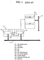
- FIG. 1 is a block diagram illustrative of a configuration of a data addressing unit and a data memory space used in a digital signal processor.
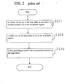
- FIG. 2 is a flow chart illustrative of a conventional operation of the filter processings.
- a data addressing unit 106 has a module register 108, a data pointer register 107 and an arithmetic and logic unit 109.
- the module register 108 is connected to a main bus 110.
- the data pointer register 107 is also connected to the main bus 110.
- the arithmetic and logic unit 109 is connected to the module register 108 and the data pointer register 107.
- the data pointer register 107 is also connected to a data memory space 101.
- the data memory space 101 has a ring-buffer 103 terminated with a top 104 and an end 105.
- the data memory space 101 is also connected to a data bus 102.
- a first step S601 an address for the top 104 of the ring buffer 103 as the object of the filter-process is set in the data pointer register 107, wherein the address for the top 104 of the ring buffer 103 has low bits of zero in the bit number necessary for representing buffer size.
- the address of the top 104 of the ring-buffer 103 is not actively determined in the filter-processing. A fixed address is used which has been allocated by a designer for the filter-processing.
- a buffer size of the ring-buffer is set in the ring-buffer register 108.
- a filter-processing is carried out by sequential accesses to the ring-buffers 103. Even, during the filter-processing, a value of the data pointer register 107 for access to the ring-buffer 103 is subjected to an automatic adding operation for the address whereby the value of the data pointer register 107 is beyond the end 105 of the ring-buffer 103, then an adjustment to the address is always made by the ring buffer register 108 and the arithmetic and logic unit 109 in the data addressing unit 106 without an adjustment to the address by software.
- FIG. 3 is a flow chart illustrative of a conventional process for two filters.
- FIG. 4 is a memory map illustrative of the conventional process for two filters of FIG. 3.
- a fixed address allocated by the filter designer is set.
- a buffer size of the first ring-buffer "A" is set in the ring buffer register.
- a third step S702 as a top address of a second ring-buffer "B”, another fixed address allocated by the filter designer is set.
- a buffer size of the second ring-buffer "B" is set in the ring buffer register.
- a filer 1 is processed.
- a ring-buffer “C” is not used for the filter 1, and also parts 10-20 of the ring-buffer “A” are not used for the filter 1. Notwithstanding, the ring-buffer "C” and the parts 10-20 of the ring-buffer “A” are ensured for processing the filter 1. Accordingly, not only use memory spaces but also non-use memory spaces are ensured to correspond to the maximum value of the buffer. The non-use memory space is unavailable for the other processes than the process for the filter 1.
- a third step S703 as a top address of a third ring-buffer "C”, another fixed address allocated by the filter designer is set.
- a buffer size of the third ring-buffer "C" is set in the ring buffer register.
- a filer 2 is processed.
- the ring-buffers "B” and “C” are not used for processing the filter 2. Notwithstanding, the ring-buffers "B” and “C” are ensured for processing the filter 1. Accordingly, not only use memory spaces but also non-use memory spaces are ensured to correspond to the maximum value of the buffer. The non-use memory space is unavailable for the other processes than the process for the filter 2.
- the first problem is a low efficiency in use of the memory spaces.
- the memory space In order to execute the filter-process to the plural ring-buffers different in size from each other, the memory space is ensured corresponding to the maximum size. This memory space will remain ensured even after the filter-process. The memory space once ensured for the one filter process will be unavailable for any other processes.
- the second problem is a complicated memory management.
- the low bit of the address for the top of the ring buffer is zero in the bit number necessary for representing buffer size.
- the calculation of those addresses is made by the filter-designer for every ring-buffers so as to place the ring-buffers at fixed ring-buffer addresses.
- the first present invention provides a method of processing at least a filter by ensuring a ring-buffer memory space in a digital signal processor, wherein if ring-buffer data stored in the ring-buffer memory space becomes no longer necessary after a filter-process is carried out, the ring-buffer memory space is released.
- the first present invention provides a method of processing at least a filter by ensuring a ring-buffer memory space in a digital signal processor, wherein if ring-buffer data stored in the ring-buffer memory space becomes no longer necessary after a filter-process is carried out, the ring-buffer memory space is released.
- a single filter is processes, and the method comprises the steps of : setting a current address at a top of a data region in a ring-buffer memory space for placement of ring-buffer data to carry out an initialization ; calculating a top address of a ring-buffer as an object for a filter-process to calculate a ring-buffer address ; setting the calculated top address at the calculated ring-buffer address ; ensuring a ring-buffer memory space corresponding to a ring-buffer size from the top address of the ring-buffer ; setting the ring-buffer size in a ring-buffer register ; carrying out a filter-process ; and releasing the ring-buffer memory space if the ring-buffer data becomes no longer necessary after the filter-process.
- the step of calculating the ring-buffer address comprises the steps of : carrying out a decrement to a buffer size of a ring-buffer as an object of a filter-process ; executing calculation of a left shift number, where non-zero bit is MSB, on the basis of a value of the buffer size in accordance with a normalization instruction of a digital signal processor ; subtracting the left shift number from a bit number corresponding to a register width in order to obtain a necessary bit number for representing the ring-buffer size ; shifting a numerical "1" in a left direction by the necessary bit number for representing the ring-buffer size ; subjecting the shifted value to a decrement so that bits corresponding to the necessary bit number from an LSB side are made into 1 to calculate mask data as mask values ; masking a current address in a data memory space by the mask data ; and confirming whether or not the masked address is 0, and if the masked address is 0, then the current address
- first and second filters are processed, and the method comprises the steps of : setting a current address at a top of a data region in a ring-buffer memory space for placement of ring-buffer data to carry out an initialization ; calculating a first top address of a first ring-buffer as a first object for a first filter-process to calculate a first ring-buffer address ; setting the calculated first top address at the calculated first ring-buffer address ; ensuring a first ring-buffer memory space corresponding to a first ring-buffer size from the first top address of the first ring-buffer ; setting the first ring-buffer size in a first ring-buffer register ; calculating a second top address of a second ring-buffer as the first object for the first filter-process to calculate a second ring-buffer address ; setting the calculated second top address at the calculated second ring-buffer address ; ensuring a second ring-buffer memory space corresponding to
- each of the steps of calculating the first, second and third ring-buffer addresses comprises the steps of : carrying out a decrement to a buffer size of a ring-buffer as an object of a filter-process ; executing calculation of a left shift number, where non-zero bit is MSB, on the basis of a value of the buffer size in accordance with a normalization instruction of a digital signal processor ; subtracting the left shift number from a bit number corresponding to a register width in order to obtain a necessary bit number for representing the ring-buffer size ; shifting a numerical "1" in a left direction by the necessary bit number for representing the ring-buffer size ; subjecting the shifted value to a decrement so that bits corresponding to the necessary bit number from an LSB side are made into 1 to calculate mask data as mask values ; masking a current address in a data memory space by the mask data ; and confirming whether or not the masked address is 0, and if the masked
- the second present invention provides a system for processing at least a filter by ensuring a ring-buffer memory space in a digital signal processor, wherein the system has an element for releasing the ring-buffer memory space if ring-buffer data stored in the ring-buffer memory space becomes no longer necessary after a filter-process is carried out.
- a single filter is processes by the system, and the system comprises : an element for setting a current address at a top of a data region in a ring-buffer memory space for placement of ring-buffer data to carry out an initialization ; an element for calculating a top address of a ring-buffer as an object for a filter-process to calculate a ring-buffer address ; an element for setting the calculated top address at the calculated ring-buffer address ; an element for ensuring a ring-buffer memory space corresponding to a ring-buffer size from the top address of the ring-buffer ; an element for setting the ring-buffer size in a ring-buffer register ; an element for carrying out a filter-process ; and an element for releasing the ring-buffer memory space if the ring-buffer data becomes no longer necessary after the filter-process.
- the element for calculating the ring-buffer address further comprises : an element for carrying out a decrement to a buffer size of a ring-buffer as an object of a filter-process ; an element for executing calculation of a left shift number, where non-zero bit is MSB, on the basis of a value of the buffer size in accordance with a normalization instruction of a digital signal processor ; an element for subtracting the left shift number from a bit number corresponding to a register width in order to obtain a necessary bit number for representing the ring-buffer size ; an element for shifting a numerical "1" in a left direction by the necessary bit number for representing the ring-buffer size ; an element for subjecting the shifted value to a decrement so that bits corresponding to the necessary bit number from an LSB side are made into 1 to calculate mask data as mask values ; an element for masking a current address in a data memory space by the mask data ; and an element for confirming whether or not the
- first and second filters are processed by the system, and the system comprises : an element for setting a current address at a top of a data region in a ring-buffer memory space for placement of ring-buffer data to carry out an initialization ; an element for calculating a first top address of a first ring-buffer as a first object for a first filter-process to calculate a first ring-buffer address ; an element for setting the calculated first top address at the calculated first ring-buffer address ; an element for ensuring a first ring-buffer memory space corresponding to a first ring-buffer size from the first top address of the first ring-buffer ; an element for setting the first ring-buffer size in a first ring-buffer register ; an element for calculating a second top address of a second ring-buffer as the first object for the first filter-process to calculate a second ring-buffer address ; an element for setting the calculated second top address at the calculated second ring-
- each of the elements for calculating the first, second and third ring-buffer addresses further comprises : an element for carrying out a decrement to a buffer size of a ring-buffer as an object of a filter-process ; an element for executing calculation of a left shift number, where non-zero bit is MSB, on the basis of a value of the buffer size in accordance with a normalization instruction of a digital signal processor ; an element for subtracting the left shift number from a bit number corresponding to a register width in order to obtain a necessary bit number for representing the ring-buffer size ; an element for shifting a numerical "1" in a left direction by the necessary bit number for representing the ring-buffer size ; an element for subjecting the shifted value to a decrement so that bits corresponding to the necessary bit number from an LSB side are made into 1 to calculate mask data as mask values ; an element for masking a current address in a data memory space by the mask data ; and an element for
- the third present invention provides a storage medium for storing a computer-readable program for processing at least a filter by ensuring a ring-buffer memory space in a digital signal processor, wherein the program releases the ring-buffer memory space if ring-buffer data stored in the ring-buffer memory space becomes no longer necessary after a filter-process is carried out.
- a single filter is processes, and the program comprises the steps of : setting a current address at a top of a data region in a ring-buffer memory space for placement of ring-buffer data to carry out an initialization ; calculating a top address of a ring-buffer as an object for a filter-process to calculate a ring-buffer address ; setting the calculated top address at the calculated ring-buffer address ; ensuring a ring-buffer memory space corresponding to a ring-buffer size from the top address of the ring-buffer ; setting the ring-buffer size in a ring-buffer register ; carrying out a filter-process ; and releasing the ring-buffer memory space if the ring-buffer data becomes no longer necessary after the filter-process.
- the step of calculating the ring-buffer address comprises the steps of : carrying out a decrement to a buffer size of a ring-buffer as an object of a filter-process ; executing calculation of a left shift number, where non-zero bit is MSB, on the basis of a value of the buffer size in accordance with a normalization instruction of a digital signal processor ; subtracting the left shift number from a bit number corresponding to a register width in order to obtain a necessary bit number for representing the ring-buffer size ; shifting a numerical "1" in a left direction by the necessary bit number for representing the ring-buffer size ; subjecting the shifted value to a decrement so that bits corresponding to the necessary bit number from an LSB side are made into 1 to calculate mask data as mask values ; masking a current address in a data memory space by the mask data ; and confirming whether or not the masked address is 0, and if the masked address is 0, then the current address
- first and second filters are processed, and the program comprises the steps of : setting a current address at a top of a data region in a ring-buffer memory space for placement of ring-buffer data to carry out an initialization ; calculating a first top address of a first ring-buffer as a first object for a first filter-process to calculate a first ring-buffer address ; setting the calculated first top address at the calculated first ring-buffer address ; ensuring a first ring-buffer memory space corresponding to a first ring-buffer size from the first top address of the first ring-buffer ; setting the first ring-buffer size in a first ring-buffer register ; calculating a second top address of a second ring-buffer as the first object for the first filter-process to calculate a second ring-buffer address ; setting the calculated second top address at the calculated second ring-buffer address ; ensuring a second ring-buffer memory space corresponding to
- each of the steps of calculating the first, second and third ring-buffer addresses comprises the steps of : carrying out a decrement to a buffer size of a ring-buffer as an object of a filter-process ; executing calculation of a left shift number, where non-zero bit is MSB, on the basis of a value of the buffer size in accordance with a normalization instruction of a digital signal processor ; subtracting the left shift number from a bit number corresponding to a register width in order to obtain a necessary bit number for representing the ring-buffer size ; shifting a numerical "1" in a left direction by the necessary bit number for representing the ring-buffer size ; subjecting the shifted value to a decrement so that bits corresponding to the necessary bit number from an LSB side are made into 1 to calculate mask data as mask values ; masking a current address in a data memory space by the mask data ; and confirming whether or not the masked address is 0, and if the masked
- FIG. 5 is a block diagram illustrative of a configuration of a data addressing unit and a data memory space used in a digital signal processor in a novel filter-processes in a first embodiment in accordance with the present invention.
- a data memory space 101 is connected to a data bus 102 independent from a main bus 101 for the purpose of parallel processings for operations and data access.
- the data memory space 101 has a ring-buffer 103 terminated with a top 104 and an end 105.
- a data addressing unit 106 has a module register 108, a data pointer register 107 and an arithmetic and logic unit 109.
- the data pointer register 107 is also connected to the data memory space 101, so that the data pointer register 107 serves as an exclusive register for the data access to the data memory space 101.
- the arithmetic and logic unit 109 is connected to the data pointer register 107, so that after the data access, then a value of the data pointer register 107 is sent to the arithmetic and logic unit 109, so that the value is automatically subjected to an automatic address add operation by the arithmetic and logic unit 109.
- the module register 108 is connected to a main bus 110.
- the data pointer register 107 is also connected to the main bus 110.
- the arithmetic and logic unit 109 is connected to the module register 108.
- the module register 108 stores ring buffer sizes of the ring buffers.
- the arithmetic and logic unit 109 compares the added value with a value of the module register 108. If the added value exceeds the value of the module register 108, then the value of the data pointer register 107 is returned to the top 104 of the ring-buffer 103, provided that a hardware restriction makes it necessary that the address of the top 104 of the ring-buffer 103 is zero in low bit number necessary for representing the buffer size by the module register 108. For example, if the ring-buffer size is 8 words, the necessary bit number for representation is 5 bits, for which reason five lower bits of the address of the top 104 of the ring-buffer 103 is zero. It is impossible that the buffer size is zero, for which reason zero is considered to be buffer size 1. In this case, the necessary bit number for representing the buffer size 8 is 4 bits.
- FIG. 6 is a flow chart illustrative of a novel operation of the filter processings, wherein a single filter uses a single ring-buffer, in a first embodiment in accordance with the present invention.
- FIG. 7 is a flow chart illustrative of a novel operation of calculation of a ring-buffer address involved in the filter processings of FIG. 6.
- a current address is set at a top of a data region of a memory for placing a ring-buffer data thereat for initialization.
- a top address of the ring-buffer as an object of the filter-process is calculated in the following processes shown in FIG. 7.
- a decrement is made to the buffer size of the ring-buffer as the object of the filter-process.
- a left shift number is calculated by a normalization instruction of the digital signal processor.
- a step S303 the above calculated left shift number is subtracted from the bit number corresponding to a register width in order to obtain the necessary bit number for representing the ring-buffer size.
- a numerical "1" is shifted in left direction by the necessary bit number for representing the ring-buffer size.
- a step S305 the above shifted value is subjected to the decrement so that bits corresponding to the above necessary bit number from the LSB side are made into 1 to calculate a mask data as a mask value.
- a current address in the data memory space is masked by the above mask data.
- a step S307 it is confirmed whether or not the masked address is 0. If the masked address is 0, then the process will enter into a step S308. If the masked address is not 0, then the process will enter into a step S309.
- a step S308 since the masked address is 0, then the above current address becomes a top address of the ring-buffer, for which the memory space is ensured, thereby calculating the top address of the ring-buffer as the object to the filter process.
- a step S309 since the masked address is not 0, then for the current address, bits corresponding to the above mask value become 0 and further the current address is added with a value obtained by increment to the mask value by the one-bit so that the added current address becomes a top address of the ring-buffer, for which the memory space is ensured, thereby calculating the top address of the ring-buffer as the object to the filter process.
- the calculated top address is set in the ring-buffer address.
- step S202 there is ensured a memory space corresponding to the ring-buffer size from the calculated top address.
- the ring-buffer size is set in the ring-buffer register.
- step S204 the filter-process is carried out.
- step S205 if the ring-buffer data are no longer necessary after the filter-process has been carried out, then there is released the secured memory space for the ring-buffer.
- the top address to be ensured is added with the size to be ensured in order to renew the current address for the next cycle, whilst non-renewed current address is stored.
- the stored non-renewed current address is utilized to be renewed into the top of the memory space to be released. It is also possible to store the buffer size in place of the current address.
- FIG. 8 is a flow chart illustrative of a novel operation of the filter processings, wherein two filter use two ring-buffers in accordance with the present invention.
- FIG. 9 is a memory map illustrative of the novel process for two filters of FIG. 8.
- the ring-buffers "A” and “B” are processed.
- the ring-buffer “A” varies in the range of size from 10 to 20.
- the size is assumed to be 10.
- the ring-buffer "B” varies in the range of size from 40 to 80. In the followings, the size is assumed to be 80.
- the ring-buffer "C” and “B” is processed. The size is assumed to be 20.
- a current address is set at a top of a data region of a memory for placing a ring-buffer data thereat for initialization.
- a top address of the ring-buffer "A" as an object of the filter-1-process is calculated in the following processes shown in FIG. 7.
- a decrement is made to the buffer size of the ring-buffer "A" as the object of the filter-1-process.
- a left shift number is calculated by a normalization instruction of the digital signal processor.
- a step S303 the above calculated left shift number is subtracted from the bit number corresponding to a register width in order to obtain the necessary bit number for representing the first ring-buffer size of the ring-buffer "A".
- a numerical "1" is shifted in left direction by the necessary bit number for representing the first ring-buffer size of the ring-buffer "A".
- a step S305 the above shifted value is subjected to the decrement so that bits corresponding to the above necessary bit number from the LSB side are made into 1 to calculate a mask data as a mask value.
- a current address in the data memory space is masked by the above mask data.
- a step S307 it is confirmed whether or not the masked address is 0. If the masked address is 0, then the process will enter into a step S308. If the masked address is not 0, then the process will enter into a step S309.
- a step S308 since the masked address is 0, then the above current address becomes a top address of the ring-buffer, for which the memory space "A" is ensured, thereby calculating the top address of the ring-buffer "A" as the object to the filter process.
- a step S309 since the masked address is not 0, then for the current address, bits corresponding to the above mask value become 0 and further the current address is added with a value obtained by increment to the mask value by the one-bit so that the added current address becomes a top address of the ring-buffer "A", for which the memory space "A” is ensured, thereby calculating the top address of the ring-buffer "A" as the object to the filter process.
- step S401 the calculated top address of the ring-buffer "A" is set in the ring-buffer address.
- step S402 there is ensured a memory space "A" corresponding to the ring-buffer size from the calculated top address of the ring-buffer "A".
- the current address is set in the next to the ring-buffer size.
- the ring-buffer size of the ring-buffer "A" is set in the ring-buffer register.
- a top address of the ring-buffer "B" as an object of the filter-1-process is calculated in the following processes shown in FIG. 7.
- a decrement is made to the buffer size of the ring-buffer "B" as the object of the filter-1-process.
- a left shift number is calculated by a normalization instruction of the digital signal processor.
- a step S303 the above calculated left shift number is subtracted from the bit number corresponding to a register width in order to obtain the necessary bit number for representing the second ring-buffer size of the ring-buffer "B".
- a numerical "1" is shifted in left direction by the necessary bit number for representing the second ring-buffer size of the ring-buffer "B".
- a step S305 the above shifted value is subjected to the decrement so that bits corresponding to the above necessary bit number from the LSB side are made into 1 to calculate a mask data as a mask value.
- a current address in the data memory space is masked by the above mask data.
- a step S307 it is confirmed whether or not the masked address is 0. If the masked address is 0, then the process will enter into a step S308. If the masked address is not 0, then the process will enter into a step S309.
- a step S308 since the masked address is 0, then the above current address becomes a top address of the ring-buffer, for which the memory space "B" is ensured, thereby calculating the top address of the ring-buffer "B" as the object to the filter process.
- a step S309 since the masked address is not 0, then for the current address, bits corresponding to the above mask value become 0 and further the current address is added with a value obtained by increment to the mask value by the one-bit so that the added current address becomes a top address of the ring-buffer "B", for which the memory space "B” is ensured, thereby calculating the top address of the ring-buffer "B" as the object to the filter process.
- step S404 the calculated top address of the ring-buffer "B" is set in the ring-buffer address.
- step S405 there is ensured a memory space "B" corresponding to the ring-buffer size from the calculated top address of the ring-buffer "B".
- the current address is set in the next to the ring-buffer size.
- the ring-buffer size of the ring-buffer "B" is set in the ring-buffer register.
- the filter-1-process for processing the filter 1 is carried out with reference to the ring-buffers "A" and "B".
- step S408 if the ring-buffer data of the ring-buffer "A" are no longer necessary after the filter-process has been carried out, then there is released the secured memory space "A" for the ring-buffer "A".
- step S409 if the ring-buffer data of the ring-buffer "B" are no longer necessary after the filter-process has been carried out, then there is released the secured memory space “B" for the ring-buffer "B".
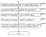
- a top address of the ring-buffer "C" as an object of the filter-2-process is calculated in the following processes shown in FIG. 7.
- a decrement is made to the buffer size of the ring-buffer "C" as the object of the filter-2-process.
- a left shift number is calculated by a normalization instruction of the digital signal processor.
- a step S303 the above calculated left shift number is subtracted from the bit number corresponding to a register width in order to obtain the necessary bit number for representing the third ring-buffer size of the ring-buffer "C".
- a numerical "1" is shifted in left direction by the necessary bit number for representing the third ring-buffer size of the ring-buffer "C".
- a step S305 the above shifted value is subjected to the decrement so that bits corresponding to the above necessary bit number from the LSB side are made into 1 to calculate a mask data as a mask value.
- a current address in the data memory space is masked by the above mask data.
- a step S307 it is confirmed whether or not the masked address is 0. If the masked address is 0, then the process will enter into a step S308. If the masked address is not 0, then the process will enter into a step S309.
- a step S308 since the masked address is 0, then the above current address becomes a top address of the ring-buffer, for which the memory space "C" is ensured, thereby calculating the top address of the ring-buffer "C" as the object to the filter process.
- a step S309 since the masked address is not 0, then for the current address, bits corresponding to the above mask value become 0 and further the current address is added with a value obtained by increment to the mask value by the one-bit so that the added current address becomes a top address of the ring-buffer "C", for which the memory space "C” is ensured, thereby calculating the top address of the ring-buffer "C” as the object to the filter process.
- step S410 the calculated top address of the ring-buffer "C" is set in the ring-buffer address.
- step S411 there is ensured a memory space "C" corresponding to the ring-buffer size from the calculated top address of the ring-buffer "C".
- the current address is set in the next to the ring-buffer size.
- the ring-buffer size of the ring-buffer "C” is set in the ring-buffer register.
- step S413 the filter-2-process for processing the filter 2 is carried out with reference to the ring-buffer "C".
- step S414 if the ring-buffer data of the ring-buffer "C" are no longer necessary after the filter-process has been carried out, then there is released the secured memory space “C” for the ring-buffer "C".
- the top address of the ring-buffer is calculated to actively ensure and release the memory space to prevent ensuring the unnecessary memory space, thereby improving the efficiency in use of the memory space.
- the above present invention provides the following effects.
- the first effect is to improve the memory efficiency.
- the memory space corresponding to the maximum value of the ring-buffer is fixedly ensured even after the ensured memory space has become no longer necessary.
- the unnecessary memory space is released so that substantially no buffer region in non-use is present.
- the present invention provides 25% reduction in the used size.
- the second effect of the present invention is to allow shortening the necessary time period for development to the filter-process program.
- the calculation of the address of the ring-buffer and ensuring the memory space are made by the programs.
- the filter-designer is allowed to design the filter processes without considering the memory layout of the ring-buffer. Further, it is allowed that the data for the ring-buffers and other data co-exist in the single data region, whereby making it convenience for the memory management.
Landscapes
- Engineering & Computer Science (AREA)
- Theoretical Computer Science (AREA)
- Physics & Mathematics (AREA)
- General Engineering & Computer Science (AREA)
- General Physics & Mathematics (AREA)
- Image Input (AREA)
- Image Processing (AREA)
- Information Transfer Systems (AREA)
- Memory System (AREA)
Abstract
Description
Claims (15)
- A method of processing at least a filter by ensuring a ring-buffer memory space in a digital signal processor, characterized in that if ring-buffer data stored in said ring-buffer memory space becomes no longer necessary after a filter-process is carried out, said ring-buffer memory space is released.
- The method as claimed in claim 1, characterized in that a single filter is processes, and said method comprises the steps of :setting a current address at a top of a data region in a ring-buffer memory space for placement of ring-buffer data to carry out an initialization ;calculating a top address of a ring-buffer as an object for a filter-process to calculate a ring-buffer address ;setting said calculated top address at said calculated ring-buffer address ;ensuring a ring-buffer memory space corresponding to a ring-buffer size from said top address of said ring-buffer ;setting said ring-buffer size in a ring-buffer register ;carrying out a filter-process ; andreleasing said ring-buffer memory space if said ring-buffer data becomes no longer necessary after said filter-process.
- The method as claimed in claim 2, characterized in that said step of calculating said ring-buffer address comprises the steps of :carrying out a decrement to a buffer size of a ring-buffer as an object of a filter-process ;executing calculation of a left shift number, where non-zero bit is MSB, on the basis of a value of said buffer size in accordance with a normalization instruction of a digital signal processor ;subtracting said left shift number from a bit number corresponding to a register width in order to obtain a necessary bit number for representing said ring-buffer size ;shifting a numerical "1" in a left direction by said necessary bit number for representing said ring-buffer size ;subjecting said shifted value to a decrement so that bits corresponding to said necessary bit number from an LSB side are made into 1 to calculate mask data as mask values ;masking a current address in a data memory space by said mask data ; andconfirming whether or not said masked address is 0, and if said masked address is 0, then said current address becomes a top address of said ring-buffer, for which said memory space is ensured, thereby calculating a top address of said ring-buffer as said object to said filter process, and if said masked address is not 0, then for said current address, bits corresponding to the above mask value become 0 and further said current address is added with a value obtained by increment to said mask value by the one-bit so that said added current address becomes a top address of said ring-buffer, for which said memory space is ensured, thereby calculating said top address of said ring-buffer as said object to said filter process.
- The method as claimed in claim 1, characterized in that first and second filters are processed, and said method comprises the steps of :setting a current address at a top of a data region in a ring-buffer memory space for placement of ring-buffer data to carry out an initialization ;calculating a first top address of a first ring-buffer as a first object for a first filter-process to calculate a first ring-buffer address ;setting said calculated first top address at said calculated first ring-buffer address ;ensuring a first ring-buffer memory space corresponding to a first ring-buffer size from said first top address of said first ring-buffer ;setting said first ring-buffer size in a first ring-buffer register ;calculating a second top address of a second ring-buffer as said first object for said first filter-process to calculate a second ring-buffer address ;setting said calculated second top address at said calculated second ring-buffer address ;ensuring a second ring-buffer memory space corresponding to a second ring-buffer size from said second top address of said second ring-buffer ;setting said second ring-buffer size in a second ring-buffer register ;carrying out a first filter-process ; andreleasing said first and second ring-buffer memory spaces if said first and second ring-buffer data become no longer necessary after said first filter-process to renew a current address ;calculating a third top address of a third ring-buffer as a second object for a second filter-process to calculate a third ring-buffer address ;setting said calculated third top address at said calculated third ring-buffer address ;ensuring a third ring-buffer memory space corresponding to a third ring-buffer size from said third top address of said third ring-buffer ;setting said third ring-buffer size in a third ring-buffer register ;carrying out a second filter-process ; andreleasing said third ring-buffer memory space if said third ring-buffer data become no longer necessary after said second filter-process to renew the current address.
- The method as claimed in claim 4, characterized in that each of said steps of calculating said first, second and third ring-buffer addresses comprises the steps of :carrying out a decrement to a buffer size of a ring-buffer as an object of a filter-process ;executing calculation of a left shift number, where non-zero bit is MSB, on the basis of a value of said buffer size in accordance with a normalization instruction of a digital signal processor ;subtracting said left shift number from a bit number corresponding to a register width in order to obtain a necessary bit number for representing said ring-buffer size ;shifting a numerical "1" in a left direction by said necessary bit number for representing said ring-buffer size ;subjecting said shifted value to a decrement so that bits corresponding to said necessary bit number from an LSB side are made into 1 to calculate mask data as mask values ;masking a current address in a data memory space by said mask data ; andconfirming whether or not said masked address is 0, and if said masked address is 0, then said current address becomes a top address of said ring-buffer, for which said memory space is ensured, thereby calculating a top address of said ring-buffer as said object to said filter process, and if said masked address is not 0, then for said current address, bits corresponding to the above mask value become 0 and further said current address is added with a value obtained by increment to said mask value by the one-bit so that said added current address becomes a top address of said ring-buffer, for which said memory space is ensured, thereby calculating said top address of said ring-buffer as said object to said filter process.
- A system for processing at least a filter by ensuring a ring-buffer memory space in a digital signal processor, characterized in that said system has means for releasing said ring-buffer memory space if ring-buffer data stored in said ring-buffer memory space becomes no longer necessary after a filter-process is carried out.
- The system as claimed in claim 6, characterized in that a single filter is processes by said system, and said system comprises :means for setting a current address at a top of a data region in a ring-buffer memory space for placement of ring-buffer data to carry out an initialization ;means for calculating a top address of a ring-buffer as an object for a filter-process to calculate a ring-buffer address ;means for setting said calculated top address at said calculated ring-buffer address ;means for ensuring a ring-buffer memory space corresponding to a ring-buffer size from said top address of said ring-buffer ;means for setting said ring-buffer size in a ring-buffer register ;means for carrying out a filter-process ; andmeans for releasing said ring-buffer memory space if said ring-buffer data becomes no longer necessary after said filter-process.
- The system as claimed in claim 7, characterized in that said means for calculating said ring-buffer address further comprises :means for carrying out a decrement to a buffer size of a ring-buffer as an object of a filter-process ;means for executing calculation of a left shift number, where non-zero bit is MSB, on the basis of a value of said buffer size in accordance with a normalization instruction of a digital signal processor ;means for subtracting said left shift number from a bit number corresponding to a register width in order to obtain a necessary bit number for representing said ring-buffer size ;means for shifting a numerical "1" in a left direction by said necessary bit number for representing said ring-buffer size ;means for subjecting said shifted value to a decrement so that bits corresponding to said necessary bit number from an LSB side are made into 1 to calculate mask data as mask values ;means for masking a current address in a data memory space by said mask data ; andmeans for confirming whether or not said masked address is 0, and if said masked address is 0, then said current address becomes a top address of said ring-buffer, for which said memory space is ensured, thereby calculating a top address of said ring-buffer as said object to said filter process, and if said masked address is not 0, then for said current address, bits corresponding to the above mask value become 0 and further said current address is added with a value obtained by increment to said mask value by the one-bit so that said added current address becomes a top address of said ring-buffer, for which said memory space is ensured, thereby calculating said top address of said ring-buffer as said object to said filter process.
- The system as claimed in claim 6, characterized in that first and second filters are processed by said system, and said system comprises :means for setting a current address at a top of a data region in a ring-buffer memory space for placement of ring-buffer data to carry out an initialization ;means for calculating a first top address of a first ring-buffer as a first object for a first filter-process to calculate a first ring-buffer address ;means for setting said calculated first top address at said calculated first ring-buffer address ;means for ensuring a first ring-buffer memory space corresponding to a first ring-buffer size from said first top address of said first ring-buffer ;means for setting said first ring-buffer size in a first ring-buffer register ;means for calculating a second top address of a second ring-buffer as said first object for said first filter-process to calculate a second ring-buffer address ;means for setting said calculated second top address at said calculated second ring-buffer address ;means for ensuring a second ring-buffer memory space corresponding to a second ring-buffer size from said second top address of said second ring-buffer ;means for setting said second ring-buffer size in a second ring-buffer register ;means for carrying out a first filter-process ; andmeans for releasing said first and second ring-buffer memory spaces if said first and second ring-buffer data become no longer necessary after said first filter-process to renew a current address ;means for calculating a third top address of a third ring-buffer as a second object for a second filter-process to calculate a third ring-buffer address ;means for setting said calculated third top address at said calculated third ring-buffer address ;means for ensuring a third ring-buffer memory space corresponding to a third ring-buffer size from said third top address of said third ring-buffer ;means for setting said third ring-buffer size in a third ring-buffer register ;means for carrying out a second filter-process ; andmeans for releasing said third ring-buffer memory space if said third ring-buffer data become no longer necessary after said second filter-process to renew the current address.
- The system as claimed in claim 9, characterized in that each of said means for calculating said first, second and third ring-buffer addresses further comprises :means for carrying out a decrement to a buffer size of a ring-buffer as an object of a filter-process ;means for executing calculation of a left shift number, where non-zero bit is MSB, on the basis of a value of said buffer size in accordance with a normalization instruction of a digital signal processor ;means for subtracting said left shift number from a bit number corresponding to a register width in order to obtain a necessary bit number for representing said ring-buffer size ;means for shifting a numerical "1" in a left direction by said necessary bit number for representing said ring-buffer size ;means for subjecting said shifted value to a decrement so that bits corresponding to said necessary bit number from an LSB side are made into 1 to calculate mask data as mask values ;means for masking a current address in a data memory space by said mask data ; andmeans for confirming whether or not said masked address is 0, and if said masked address is 0, then said current address becomes a top address of said ring-buffer, for which said memory space is ensured, thereby calculating a top address of said ring-buffer as said object to said filter process, and if said masked address is not 0, then for said current address, bits corresponding to the above mask value become 0 and further said current address is added with a value obtained by increment to said mask value by the one-bit so that said added current address becomes a top address of said ring-buffer, for which said memory space is ensured, thereby calculating said top address of said ring-buffer as said object to said filter process.
- A storage medium for storing a computer-readable program for processing at least a filter by ensuring a ring-buffer memory space in a digital signal processor, characterized in that said program releases said ring-buffer memory space if ring-buffer data stored in said ring-buffer memory space becomes no longer necessary after a filter-process is carried out.
- The storage medium as claimed in claim 11, characterized in that a single filter is processes, and said program comprises the steps of :setting a current address at a top of a data region in a ring-buffer memory space for placement of ring-buffer data to carry out an initialization ;calculating a top address of a ring-buffer as an object for a filter-process to calculate a ring-buffer address ;setting said calculated top address at said calculated ring-buffer address ;ensuring a ring-buffer memory space corresponding to a ring-buffer size from said top address of said ring-buffer ;setting said ring-buffer size in a ring-buffer register ;carrying out a filter-process ; andreleasing said ring-buffer memory space if said ring-buffer data becomes no longer necessary after said filter-process.
- The storage medium as claimed in claim 12, characterized in that said step of calculating said ring-buffer address comprises the steps of :carrying out a decrement to a buffer size of a ring-buffer as an object of a filter-process ;executing calculation of a left shift number, where non-zero bit is MSB, on the basis of a value of said buffer size in accordance with a normalization instruction of a digital signal processor ;subtracting said left shift number from a bit number corresponding to a register width in order to obtain a necessary bit number for representing said ring-buffer size ;shifting a numerical "1" in a left direction by said necessary bit number for representing said ring-buffer size ;subjecting said shifted value to a decrement so that bits corresponding to said necessary bit number from an LSB side are made into 1 to calculate mask data as mask values ;masking a current address in a data memory space by said mask data ; andconfirming whether or not said masked address is 0, and if said masked address is 0, then said current address becomes a top address of said ring-buffer, for which said memory space is ensured, thereby calculating a top address of said ring-buffer as said object to said filter process, and if said masked address is not 0, then for said current address, bits corresponding to the above mask value become 0 and further said current address is added with a value obtained by increment to said mask value by the one-bit so that said added current address becomes a top address of said ring-buffer, for which said memory space is ensured, thereby calculating said top address of said ring-buffer as said object to said filter process.
- The storage medium as claimed in claim 11, characterized in that first and second filters are processed, and said program comprises the steps of :setting a current address at a top of a data region in a ring-buffer memory space for placement of ring-buffer data to carry out an initialization ;calculating a first top address of a first ring-buffer as a first object for a first filter-process to calculate a first ring-buffer address ;setting said calculated first top address at said calculated first ring-buffer address ;ensuring a first ring-buffer memory space corresponding to a first ring-buffer size from said first top address of said first ring-buffer ;setting said first ring-buffer size in a first ring-buffer register ;calculating a second top address of a second ring-buffer as said first object for said first filter-process to calculate a second ring-buffer address ;setting said calculated second top address at said calculated second ring-buffer address ;ensuring a second ring-buffer memory space corresponding to a second ring-buffer size from said second top address of said second ring-buffer ;setting said second ring-buffer size in a second ring-buffer register ;carrying out a first filter-process ; andreleasing said first and second ring-buffer memory spaces if said first and second ring-buffer data become no longer necessary after said first filter-process to renew a current address ;calculating a third top address of a third ring-buffer as a second object for a second filter-process to calculate a third ring-buffer address ;setting said calculated third top address at said calculated third ring-buffer address ;ensuring a third ring-buffer memory space corresponding to a third ring-buffer size from said third top address of said third ring-buffer ;setting said third ring-buffer size in a third ring-buffer register;carrying out a second filter-process ; andreleasing said third ring-buffer memory space if said third ring-buffer data become no longer necessary after said second filter-process to renew the current address.
- The storage medium as claimed in claim 14, characterized in that each of said steps of calculating said first, second and third ring-buffer addresses comprises the steps of :carrying out a decrement to a buffer size of a ring-buffer as an object of a filter-process ;executing calculation of a left shift number, where non-zero bit is MSB, on the basis of a value of said buffer size in accordance with a normalization instruction of a digital signal processor ;subtracting said left shift number from a bit number corresponding to a register width in order to obtain a necessary bit number for representing said ring-buffer size ;shifting a numerical "1" in a left direction by said necessary bit number for representing said ring-buffer size ; subjecting said shifted value to a decrement so that bits corresponding to said necessary bit number from an LSB side are made into 1 to calculate mask data as mask values ;masking a current address in a data memory space by said mask data ; andconfirming whether or not said masked address is 0, and if said masked address is 0, then said current address becomes a top address of said ring-buffer, for which said memory space is ensured, thereby calculating a top address of said ring-buffer as said object to said filter process, and if said masked address is not 0, then for said current address, bits corresponding to the above mask value become 0 and further said current address is added with a value obtained by increment to said mask value by the one-bit so that said added current address becomes a top address of said ring-buffer, for which said memory space is ensured, thereby calculating said top address of said ring-buffer as said object to said filter process.
Applications Claiming Priority (2)
| Application Number | Priority Date | Filing Date | Title |
|---|---|---|---|
| JP11171070A JP2001005721A (en) | 1999-06-17 | 1999-06-17 | Method for filter processing by securing memory for ring buffer by dsp and its filter processing system |
| JP17107099 | 1999-06-17 |
Publications (2)
| Publication Number | Publication Date |
|---|---|
| EP1061435A2 true EP1061435A2 (en) | 2000-12-20 |
| EP1061435A3 EP1061435A3 (en) | 2004-10-27 |
Family
ID=15916485
Family Applications (1)
| Application Number | Title | Priority Date | Filing Date |
|---|---|---|---|
| EP00112799A Ceased EP1061435A3 (en) | 1999-06-17 | 2000-06-16 | Method and system for filter-processing by ensuring a memory space for a ring-buffer in digital signal processor |
Country Status (4)
| Country | Link |
|---|---|
| US (1) | US6725298B1 (en) |
| EP (1) | EP1061435A3 (en) |
| JP (1) | JP2001005721A (en) |
| SG (1) | SG90731A1 (en) |
Cited By (1)
| Publication number | Priority date | Publication date | Assignee | Title |
|---|---|---|---|---|
| WO2007048133A3 (en) * | 2005-10-20 | 2007-08-02 | Qualcomm Inc | Pointer computation method and system for a scalable, programmable circular buffer |
Families Citing this family (4)
| Publication number | Priority date | Publication date | Assignee | Title |
|---|---|---|---|---|
| JP2004171411A (en) * | 2002-11-21 | 2004-06-17 | Hitachi Global Storage Technologies Netherlands Bv | Data storage device and buffer memory management method |
| JP4661169B2 (en) * | 2003-11-14 | 2011-03-30 | ヤマハ株式会社 | Digital signal processor |
| CN114661624B (en) * | 2022-03-10 | 2026-01-30 | 北京威视锐科技有限公司 | A method, system, device, and storage medium for efficient data acquisition and storage. |
| CN115357212B (en) * | 2022-10-20 | 2023-01-13 | 瀚博半导体(上海)有限公司 | Parameter generation method and device for ring buffer and artificial intelligence chip |
Family Cites Families (12)
| Publication number | Priority date | Publication date | Assignee | Title |
|---|---|---|---|---|
| US5623621A (en) * | 1990-11-02 | 1997-04-22 | Analog Devices, Inc. | Apparatus for generating target addresses within a circular buffer including a register for storing position and size of the circular buffer |
| JP3024327B2 (en) * | 1991-12-27 | 2000-03-21 | カシオ計算機株式会社 | Digital recorder |
| JPH064458A (en) * | 1992-06-18 | 1994-01-14 | Fuji Xerox Co Ltd | Dma controller |
| JP3359987B2 (en) * | 1995-05-24 | 2002-12-24 | 松下電送システム株式会社 | Data processing device |
| KR0183173B1 (en) * | 1995-12-13 | 1999-05-15 | 윤종용 | Buffer memory control device |
| JP3486498B2 (en) * | 1996-01-10 | 2004-01-13 | キヤノン株式会社 | Buffer management method and printing apparatus using the same |
| JPH09300739A (en) * | 1996-05-16 | 1997-11-25 | Canon Inc | Reception buffer control device and recording device |
| JPH10126218A (en) * | 1996-10-15 | 1998-05-15 | Sony Corp | Sampling frequency converter |
| US6404776B1 (en) * | 1997-03-13 | 2002-06-11 | 8 × 8, Inc. | Data processor having controlled scalable input data source and method thereof |
| US6044434A (en) * | 1997-09-24 | 2000-03-28 | Sony Corporation | Circular buffer for processing audio samples |
| US6148386A (en) * | 1998-03-19 | 2000-11-14 | Lucent Technologies Inc | Address generator circuity for a circular buffer |
| US6112267A (en) * | 1998-05-28 | 2000-08-29 | Digital Equipment Corporation | Hierarchical ring buffers for buffering data between processor and I/O device permitting data writes by processor and data reads by I/O device simultaneously directed at different buffers at different levels |
-
1999
- 1999-06-17 JP JP11171070A patent/JP2001005721A/en active Pending
-
2000
- 2000-06-16 SG SG200003379A patent/SG90731A1/en unknown
- 2000-06-16 EP EP00112799A patent/EP1061435A3/en not_active Ceased
- 2000-06-19 US US09/597,900 patent/US6725298B1/en not_active Expired - Fee Related
Cited By (1)
| Publication number | Priority date | Publication date | Assignee | Title |
|---|---|---|---|---|
| WO2007048133A3 (en) * | 2005-10-20 | 2007-08-02 | Qualcomm Inc | Pointer computation method and system for a scalable, programmable circular buffer |
Also Published As
| Publication number | Publication date |
|---|---|
| SG90731A1 (en) | 2002-08-20 |
| EP1061435A3 (en) | 2004-10-27 |
| JP2001005721A (en) | 2001-01-12 |
| US6725298B1 (en) | 2004-04-20 |
Similar Documents
| Publication | Publication Date | Title |
|---|---|---|
| US11347964B2 (en) | Hardware circuit | |
| US7500028B2 (en) | DMA controller providing for ring buffer and rectangular block transfers | |
| JP3599352B2 (en) | Flexible N-way memory interleave scheme | |
| US6895459B2 (en) | Bus arbitration method employing a table of slots suitably distributed amongst bus masters | |
| EP0577101B1 (en) | Multiplier accumulator | |
| EP2804144A1 (en) | Method and device for processing input image data | |
| EP2565786A1 (en) | Information processing device and task switching method | |
| EP0997822A2 (en) | DMA control method and apparatus | |
| CN118484322B (en) | Method, computing device, medium and program product for matrix reduction computation | |
| JP4975651B2 (en) | Color conversion device | |
| EP1061435A2 (en) | Method and system for filter-processing by ensuring a memory space for a ring-buffer in digital signal processor | |
| JP2022074442A (en) | Arithmetic device and arithmetic method | |
| US6684267B2 (en) | Direct memory access controller, and direct memory access control method | |
| CN115766969B (en) | Vehicle-mounted image processing method, device, medium and computing equipment | |
| US6950922B2 (en) | Data extraction/insertion method and device in digital signal processor | |
| US5918253A (en) | Memory address generator | |
| US20130117533A1 (en) | Coprocessor having task sequence control | |
| CN116306840A (en) | Neural network computing method, device, chip, electronic equipment and storage medium | |
| JP2009093344A (en) | Microcomputer, method of using the same, and electronic control device | |
| EP1197875B1 (en) | Conditional vector operation method and device thereof | |
| US20070124563A1 (en) | Processing device, method of determining internal configuration of processing device, and processing system | |
| US6871256B2 (en) | Method and arrangement in a stack having a memory segmented into data groups having a plurality of elements | |
| JP2003271542A (en) | Direct access controller | |
| CN113362219B (en) | Image data processing method and device | |
| US20090144461A1 (en) | Method and system for configuration of a hardware peripheral |
Legal Events
| Date | Code | Title | Description |
|---|---|---|---|
| PUAI | Public reference made under article 153(3) epc to a published international application that has entered the european phase |
Free format text: ORIGINAL CODE: 0009012 |
|
| AK | Designated contracting states |
Kind code of ref document: A2 Designated state(s): AT BE CH CY DE DK ES FI FR GB GR IE IT LI LU MC NL PT SE |
|
| AX | Request for extension of the european patent |
Free format text: AL;LT;LV;MK;RO;SI |
|
| RAP1 | Party data changed (applicant data changed or rights of an application transferred) |
Owner name: NEC ELECTRONICS CORPORATION |
|
| PUAL | Search report despatched |
Free format text: ORIGINAL CODE: 0009013 |
|
| AK | Designated contracting states |
Kind code of ref document: A3 Designated state(s): AT BE CH CY DE DK ES FI FR GB GR IE IT LI LU MC NL PT SE |
|
| AX | Request for extension of the european patent |
Extension state: AL LT LV MK RO SI |
|
| 17P | Request for examination filed |
Effective date: 20040915 |
|
| AKX | Designation fees paid |
Designated state(s): DE GB |
|
| 17Q | First examination report despatched |
Effective date: 20050819 |
|
| STAA | Information on the status of an ep patent application or granted ep patent |
Free format text: STATUS: THE APPLICATION HAS BEEN REFUSED |
|
| 18R | Application refused |
Effective date: 20070720 |