EP1059759A2 - Sample timing control for demodulation of phase-modulated signals - Google Patents
Sample timing control for demodulation of phase-modulated signals Download PDFInfo
- Publication number
- EP1059759A2 EP1059759A2 EP00304656A EP00304656A EP1059759A2 EP 1059759 A2 EP1059759 A2 EP 1059759A2 EP 00304656 A EP00304656 A EP 00304656A EP 00304656 A EP00304656 A EP 00304656A EP 1059759 A2 EP1059759 A2 EP 1059759A2
- Authority
- EP
- European Patent Office
- Prior art keywords
- phase
- modulated signal
- frequency
- measure
- signal
- Prior art date
- Legal status (The legal status is an assumption and is not a legal conclusion. Google has not performed a legal analysis and makes no representation as to the accuracy of the status listed.)
- Granted
Links
Images


Classifications
-
- H—ELECTRICITY
- H04—ELECTRIC COMMUNICATION TECHNIQUE
- H04L—TRANSMISSION OF DIGITAL INFORMATION, e.g. TELEGRAPHIC COMMUNICATION
- H04L7/00—Arrangements for synchronising receiver with transmitter
- H04L7/02—Speed or phase control by the received code signals, the signals containing no special synchronisation information
- H04L7/033—Speed or phase control by the received code signals, the signals containing no special synchronisation information using the transitions of the received signal to control the phase of the synchronising-signal-generating means, e.g. using a phase-locked loop
- H04L7/0334—Processing of samples having at least three levels, e.g. soft decisions
Definitions
- the present invention relates generally to communication systems, and more particularly to communication systems such as wireless time division multiple access (TDMA) systems which utilize differential quadrature phase-shift-keyed (DQPSK) modulation or other types of phase modulation.
- TDMA wireless time division multiple access
- DQPSK differential quadrature phase-shift-keyed
- a phase modulation technique known as ⁇ /4 DQPSK is utilized to transmit digital data in certain types of communication systems, such as wireless TDMA systems.
- data is transmitted by changing the phase of a modulated signal.
- Each phase shift, over a specific period of time, is referred to as a symbol.
- the technique achieves an increase in spectral efficiency by multiplexing two signals in phase quadrature.
- the two signals, an in-phase (I) signal and a quadrature (Q) signal 90° out of phase with the I signal, are modulated onto a carrier signal to form a QPSK signal suitable for transmission.
- ⁇ /4 DQPSK the four possible phase shifts are ⁇ /4 ( ⁇ 45°) and ⁇ 3 ⁇ /4 ( ⁇ 135°), and a typical symbol period T in a conventional IS-136 or IS-54 wireless TDMA system is 41.2 ⁇ s.
- a conventional ⁇ /4 DQPSK demodulator suppresses the carrier signal and recovers the I and Q signals.
- the I and Q signals are sampled at intervals of T/4 and digitized using an analog-to-digital (A/D) converter.
- the digitized samples are then processed in a digital signal processor (DSP) to recover the phase of the symbol and its signal strength.
- FIG. 1 illustrates the T/4 sampling process for a given I or Q signal.
- the I or Q signal includes a stream of symbols, denoted N-1, N, N+1, N+2, etc. in this example. Each of the symbols of the I or Q signal is sampled at intervals of T/4, as shown.
- the T/4 sampling of symbols in a DQPSK demodulator is generally asynchronous with respect to the transmitted symbol.
- the best case situation, illustrated in FIG. 2 is when the four T/4 samples for a given symbol are taken during the most stable portion of the current symbol, i.e., symbol N.
- the worst case, illustrated in FIG. 3, occurs when one of the T/4 samples is taken at the transition between the current symbol N and a previous symbol N-1 or a subsequent symbol N+1.
- phase demodulation techniques for use with quadrature phase-shift-keyed (QPSK) signals and other types of phase-modulated signals in a communication system.
- QPSK quadrature phase-shift-keyed
- phase demodulation techniques utilize sample timing which is based at least in part on frequency information generated by frequency demodulating the phase-modulated signal.
- a phase-modulated signal is separated into first and second portions. The first portion is then phase demodulated to generate demodulated symbols, while the second portion is frequency demodulated to generate a measure of the instantaneous frequency of the phase-modulated signal. The instantaneous frequency measure is then processed to identify one or more symbol transitions, and the identified transitions are used to establish the sample timing such that proper sampling of the symbols is ensured.
- the measure of the instantaneous frequency of the phase-modulated signal may be a signal having a signature associated with a particular synchronization word utilized in the system, and may be processed to generate information which is used in a digital signal processor (DSP) or other suitable processing circuitry to generate, adjust or otherwise control a sample clock used in sampling the demodulated symbols.
- DSP digital signal processor
- the invention provides significantly improved bit error rate (BER) performance for the received data.
- BER bit error rate
- the invention can ensure a desired T/4 symbol sampling without any increase in the sampling rate or the complexity and cost of the demodulator.
- the invention is particularly well suited for use in applications such as wireless TDMA systems, it can provide similar advantages in numerous other communication system applications.
- quadrature phase-shift-keyed (QPSK) demodulation techniques QPSK
- the invention is not limited to use with any particular type of communication system, but is instead more generally applicable to any system in which it is desirable to provide improved phase demodulation performance without unduly increasing system complexity.
- QPSK quadrature phase-shift-keyed
- FIG. 4 shows a block diagram of a QPSK receiver 100 in accordance with an illustrative embodiment of the invention.
- the QPSK receiver 100 may be used to demodulate, e.g., a ⁇ /4 DQPSK signal such as that described in conjunction with FIGS. 1 through 3, or another type of QPSK signal.
- a QPSK-modulated carrier signal received via a receiver antenna 102 is down-convened in a mixer/down-convener 104, and band-pass filtered in a filter 106 to recover the QPSK signal.
- the QPSK signal is then split into two separate half-power portions in a 1:2 splitter 108.
- the first portion of the QPSK signal is applied to a conventional QPSK demodulator 110.
- the in-phase (I) and quadrature (Q) signals generated by the QPSK demodulator 110 are applied to an analog/digital (A/D) convener 112 which samples the corresponding symbols to generate a digital I and Q output for storage in a first-in first-out (FIFO) buffer 114.
- A/D analog/digital
- the second portion of the QPSK signal is passed through a frequency modulation (FM) demodulator 120 to generate a measure of the instantaneous frequency of the signal which is the derivative of the phase that contains the transmitted data.
- the FM demodulator 120 may include, e.g., an FM discriminator and/or other well-known FM demodulation circuitry.
- the instantaneous frequency output of the FM demodulator 120 is then applied to a peak detector 124.
- the peak detector generates a signature which is supplied to a digital signal processor (DSP) 126.
- DSP digital signal processor
- the DSP 126 uses this signature to generate an appropriate sample timing signal which is supplied to a sample timing generator 128.
- the sample timing signal may, e.g., indicate that the sample timing is to be advanced or retarded based on the signature from the peak detector 124.
- the DSP 126 may include, e.g., a conventional zero crossing detector and appropriate logic circuitry, in order to determine the appropriate sample timing based on the signature supplied by the peak detector 124.
- the signature can be used, e.g., to determine the start or end of a given symbol in a stream of symbols.
- one or more of the zero-crossing detector, logic circuitry or other processing elements may be implemented separately from the DSP 126.
- numerous other arrangements of circuitry may be used to generate a measure of frequency of a phase-modulated signal.
- the term "measure of frequency" as used herein is intended to include any type of frequency information which can be derived from a phase-modulated signal and utilized to control sample timing. A measure of frequency may therefore be a measure of instantaneous frequency, or another type of frequency information suitable for use in sample timing control.
- the sample timing generator 128 generates a sample clock which is applied to the A/D converter 112 and used in sampling the I and Q signal symbols.
- the timing of the sample clock is thus based on the signature supplied by the peak detector 124, and can be arranged so as to provide desired T/4 sampling within a given symbol.
- the digital I and Q output from FIFO 114 may be delivered to the DSP 126 for further processing, e.g., for generating a corresponding output digital data bitstream of a desired format.
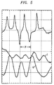
- FIG. 5 shows an example of an FM demodulator output which may be generated in the receiver of FIG. 4, along with corresponding I and Q demodulated output signals.
- Each horizontal division in the plots of FIG. 5 corresponds to 2T, i.e., two times the symbol period T.
- the uppermost signal in FIG. 5 represents the signal output of an FM discriminator circuit in the FM demodulator 120 of FIG. 4, as generated from the second portion of a QPSK signal when the modulated data corresponds to a particular synchronization word, i.e., synchronization word 1 of FIG. 7.
- the I and Q signals shown in FIG. 5 are the corresponding I and Q outputs of the QPSK demodulator 110, generated from the first portion of the same QPSK signal.
- FIG. 6 shows a corresponding simulated version of the instantaneous frequency changes associated with the symbol-to-symbol phase changes in the synchronization word 1 of FIG. 7. It can be seen that the signal output of the FM discriminator as shown in FIG. 5 corresponds closely to the simulated instantaneous frequency changes as shown in FIG. 6.
- the table of FIG. 7 shows the phase changes over a set of 14 symbols, S0 though S13, for each of six possible synchronization words, i.e., sync words 1 through 6, in an exemplary IS-136 TDMA system such as that described in the TIA/EIA 627 standard, IS-136.2-A. It should be understood that, although not explicitly shown in FIG. 7, the term " ⁇ " is implicit in the numeric values which are shown.
- Each of the synchronization words shown in the table of FIG. 7 provides a unique signature that can be used in the receiver 100 to generate appropriate sample timing information.
- the synchronization word signature at the output of the peak detector can thus be used to capture substantially the exact moment of the start of a phase change in a given symbol.
- the DSP 126 may include, e.g., a conventional zero crossing detector and appropriate logic circuitry to make such a determination.
- the phase changes given for synchronization word 1 in FIG. 7 lead to the instantaneous frequency changes shown in FIGS. 5 and 6.
- the first four symbols S0, S1, S2 and S3 have phase shifts of- ⁇ /4, - ⁇ /4, - ⁇ /4 and 3 ⁇ /4, respectively, as shown in FIG. 7.
- the output of the FM demodulator 120 is the instantaneous frequency of the signal which is the derivative of the phase, there is no need for automatic gain control or automatic frequency correction.
- the sample timing generation technique of the present invention is resistant to factors such as gain variations, fades, speed, distance, filter group delay and processing time associated with the transmitting source.
- a system in accordance with the invention may include additional elements, such as, for example, multiple base stations and mobile units, mobile switching centers (MSCs) for connecting one of more of the base stations to a public switched telephone network (PSTN), and memory or other storage elements for storing, e.g., system programs and configuration data, user data and billing information.
- MSCs mobile switching centers
- PSTN public switched telephone network
- the receiver shown herein for purposes of illustrating the invention may be implemented in many different ways, and may include a number of additional elements, e.g., additional down-converters, signal sources, filters, demodulators, detectors, signal processors, etc., configured in a conventional manner. More particularly, alternative embodiments of the invention may use different types of circuitry for generating a measure of frequency from a phase-modulated signal, and for generating appropriate sample timing based at least in part on the frequency measure.
Abstract
Description
- The present invention relates generally to communication systems, and more particularly to communication systems such as wireless time division multiple access (TDMA) systems which utilize differential quadrature phase-shift-keyed (DQPSK) modulation or other types of phase modulation.
- A phase modulation technique known as π/4 DQPSK is utilized to transmit digital data in certain types of communication systems, such as wireless TDMA systems. In accordance with this technique, data is transmitted by changing the phase of a modulated signal. Each phase shift, over a specific period of time, is referred to as a symbol. The technique achieves an increase in spectral efficiency by multiplexing two signals in phase quadrature. The two signals, an in-phase (I) signal and a quadrature (Q) signal 90° out of phase with the I signal, are modulated onto a carrier signal to form a QPSK signal suitable for transmission. In the case of π/4 DQPSK, the four possible phase shifts are ±π/4 (±45°) and ±3π/4 (±135°), and a typical symbol period T in a conventional IS-136 or IS-54 wireless TDMA system is 41.2 µs.
- A conventional π/4 DQPSK demodulator suppresses the carrier signal and recovers the I and Q signals. The I and Q signals are sampled at intervals of T/4 and digitized using an analog-to-digital (A/D) converter. The digitized samples are then processed in a digital signal processor (DSP) to recover the phase of the symbol and its signal strength. FIG. 1 illustrates the T/4 sampling process for a given I or Q signal. The I or Q signal includes a stream of symbols, denoted N-1, N, N+1, N+2, etc. in this example. Each of the symbols of the I or Q signal is sampled at intervals of T/4, as shown.
- In general, between a base station and a mobile unit in a wireless TDMA system, the T/4 sampling of symbols in a DQPSK demodulator is generally asynchronous with respect to the transmitted symbol. The best case situation, illustrated in FIG. 2, is when the four T/4 samples for a given symbol are taken during the most stable portion of the current symbol, i.e., symbol N. The worst case, illustrated in FIG. 3, occurs when one of the T/4 samples is taken at the transition between the current symbol N and a previous symbol N-1 or a subsequent symbol N+1. When taking samples asynchronously, one can guard against the worst case by comparing the quality of an odd sample pair, i.e.,
samples samples - A need therefore exists for a phase demodulation technique which can better synchronize the sampling process to the received symbols, such that improved performance can be obtained relative to the above-described conventional techniques, without significantly increasing the complexity and cost associated with the demodulation process.
- The invention provides improved phase demodulation techniques for use with quadrature phase-shift-keyed (QPSK) signals and other types of phase-modulated signals in a communication system. These phase demodulation techniques utilize sample timing which is based at least in part on frequency information generated by frequency demodulating the phase-modulated signal. In an illustrative embodiment of the invention, a phase-modulated signal is separated into first and second portions. The first portion is then phase demodulated to generate demodulated symbols, while the second portion is frequency demodulated to generate a measure of the instantaneous frequency of the phase-modulated signal. The instantaneous frequency measure is then processed to identify one or more symbol transitions, and the identified transitions are used to establish the sample timing such that proper sampling of the symbols is ensured. For example, the measure of the instantaneous frequency of the phase-modulated signal may be a signal having a signature associated with a particular synchronization word utilized in the system, and may be processed to generate information which is used in a digital signal processor (DSP) or other suitable processing circuitry to generate, adjust or otherwise control a sample clock used in sampling the demodulated symbols.
- By ensuring proper symbol timing in the demodulation process, the invention provides significantly improved bit error rate (BER) performance for the received data. For example, in a system utilizing π/4 DQPSK modulation, the invention can ensure a desired T/4 symbol sampling without any increase in the sampling rate or the complexity and cost of the demodulator. Although the invention is particularly well suited for use in applications such as wireless TDMA systems, it can provide similar advantages in numerous other communication system applications.
-
- FIGS. 1, 2 and 3 illustrate sampling of symbols in accordance with a conventional π/4 DQPSK demodulation technique.
- FIG. 4 is a block diagram of a receiver in accordance with an illustrative embodiment of the invention.
- FIG. 5 shows an FM demodulator output which may be generated in the receiver of FIG. 4, along with corresponding demodulated I and Q output signals.
- FIG. 6 shows a simulated version of the FM demodulator output of FIG. 5.
- FIG. 7 is a table showing a set of synchronization words which may be utilized to provide sample timing in the receiver of FIG. 4 for an exemplary TDMA system, in accordance with the invention.
-
- The present invention will be illustrated below in conjunction with exemplary quadrature phase-shift-keyed (QPSK) demodulation techniques. It should be understood, however, that the invention is not limited to use with any particular type of communication system, but is instead more generally applicable to any system in which it is desirable to provide improved phase demodulation performance without unduly increasing system complexity. For example, it will be apparent to those skilled in the art that the invention can be applied to demodulation of a wide variety of other types of phase-modulated signals.
- FIG. 4 shows a block diagram of a
QPSK receiver 100 in accordance with an illustrative embodiment of the invention. TheQPSK receiver 100 may be used to demodulate, e.g., a π/4 DQPSK signal such as that described in conjunction with FIGS. 1 through 3, or another type of QPSK signal. A QPSK-modulated carrier signal received via areceiver antenna 102 is down-convened in a mixer/down-convener 104, and band-pass filtered in afilter 106 to recover the QPSK signal. The QPSK signal is then split into two separate half-power portions in a 1:2splitter 108. The first portion of the QPSK signal is applied to aconventional QPSK demodulator 110. The in-phase (I) and quadrature (Q) signals generated by theQPSK demodulator 110 are applied to an analog/digital (A/D) convener 112 which samples the corresponding symbols to generate a digital I and Q output for storage in a first-in first-out (FIFO)buffer 114. - In accordance with the invention, the second portion of the QPSK signal is passed through a frequency modulation (FM)
demodulator 120 to generate a measure of the instantaneous frequency of the signal which is the derivative of the phase that contains the transmitted data. TheFM demodulator 120 may include, e.g., an FM discriminator and/or other well-known FM demodulation circuitry. The instantaneous frequency output of theFM demodulator 120 is then applied to apeak detector 124. The peak detector generates a signature which is supplied to a digital signal processor (DSP) 126. The DSP 126 uses this signature to generate an appropriate sample timing signal which is supplied to asample timing generator 128. The sample timing signal may, e.g., indicate that the sample timing is to be advanced or retarded based on the signature from thepeak detector 124. The DSP 126 may include, e.g., a conventional zero crossing detector and appropriate logic circuitry, in order to determine the appropriate sample timing based on the signature supplied by thepeak detector 124. The signature can be used, e.g., to determine the start or end of a given symbol in a stream of symbols. - In alternative embodiments, one or more of the zero-crossing detector, logic circuitry or other processing elements may be implemented separately from the DSP 126. Furthermore, numerous other arrangements of circuitry may be used to generate a measure of frequency of a phase-modulated signal. The term "measure of frequency" as used herein is intended to include any type of frequency information which can be derived from a phase-modulated signal and utilized to control sample timing. A measure of frequency may therefore be a measure of instantaneous frequency, or another type of frequency information suitable for use in sample timing control.
- The
sample timing generator 128 generates a sample clock which is applied to the A/D converter 112 and used in sampling the I and Q signal symbols. The timing of the sample clock is thus based on the signature supplied by thepeak detector 124, and can be arranged so as to provide desired T/4 sampling within a given symbol. The digital I and Q output from FIFO 114 may be delivered to the DSP 126 for further processing, e.g., for generating a corresponding output digital data bitstream of a desired format. - FIG. 5 shows an example of an FM demodulator output which may be generated in the receiver of FIG. 4, along with corresponding I and Q demodulated output signals. Each horizontal division in the plots of FIG. 5 corresponds to 2T, i.e., two times the symbol period T. The uppermost signal in FIG. 5 represents the signal output of an FM discriminator circuit in the
FM demodulator 120 of FIG. 4, as generated from the second portion of a QPSK signal when the modulated data corresponds to a particular synchronization word, i.e.,synchronization word 1 of FIG. 7. The I and Q signals shown in FIG. 5 are the corresponding I and Q outputs of theQPSK demodulator 110, generated from the first portion of the same QPSK signal. - FIG. 6 shows a corresponding simulated version of the instantaneous frequency changes associated with the symbol-to-symbol phase changes in the
synchronization word 1 of FIG. 7. It can be seen that the signal output of the FM discriminator as shown in FIG. 5 corresponds closely to the simulated instantaneous frequency changes as shown in FIG. 6. The table of FIG. 7 shows the phase changes over a set of 14 symbols, S0 though S13, for each of six possible synchronization words, i.e.,sync words 1 through 6, in an exemplary IS-136 TDMA system such as that described in the TIA/EIA 627 standard, IS-136.2-A. It should be understood that, although not explicitly shown in FIG. 7, the term "π" is implicit in the numeric values which are shown. - Each of the synchronization words shown in the table of FIG. 7 provides a unique signature that can be used in the
receiver 100 to generate appropriate sample timing information. The synchronization word signature at the output of the peak detector can thus be used to capture substantially the exact moment of the start of a phase change in a given symbol. As noted above, theDSP 126 may include, e.g., a conventional zero crossing detector and appropriate logic circuitry to make such a determination. Note that the phase changes given forsynchronization word 1 in FIG. 7 lead to the instantaneous frequency changes shown in FIGS. 5 and 6. For example, the first four symbols S0, S1, S2 and S3 have phase shifts of-π/4, -π/4, -π/4 and 3π/4, respectively, as shown in FIG. 7. As a result, the symbols S0, S1 and S2 lead to no significant change in instantaneous frequency, but symbol S3 leads to a substantial change in instantaneous frequency, as shown in FIG. 6. Detection of a signature corresponding tosynchronization word 1 can thus be used to determine the start of symbol S3, and this information can be used to establish an appropriate T/4 sample timing for subsequent received symbols. - By using such synchronization words to generate sample timing, it is possible to ensure that the π/4 sampling will correspond to the desired timing, e.g., the best case T/4 sample timing as illustrated and described in conjunction with FIG. 2. This will significantly improve the BER performance of the received data, without requiring any increase in the sample rate or the complexity and cost associated with the demodulation process.
- Since the output of the
FM demodulator 120 is the instantaneous frequency of the signal which is the derivative of the phase, there is no need for automatic gain control or automatic frequency correction. This means that the sample timing generation technique of the present invention is resistant to factors such as gain variations, fades, speed, distance, filter group delay and processing time associated with the transmitting source. - It should be emphasized that the exemplary demodulation techniques described herein are intended to illustrate the operation of the invention, and therefore should not be construed as limiting the invention to any particular embodiment or group of embodiments. For example, although well suited for implementation in a wireless TDMA system, the invention can be used in other applications. In addition, a system in accordance with the invention may include additional elements, such as, for example, multiple base stations and mobile units, mobile switching centers (MSCs) for connecting one of more of the base stations to a public switched telephone network (PSTN), and memory or other storage elements for storing, e.g., system programs and configuration data, user data and billing information. Furthermore, it will be apparent to those skilled in the art that the receiver shown herein for purposes of illustrating the invention may be implemented in many different ways, and may include a number of additional elements, e.g., additional down-converters, signal sources, filters, demodulators, detectors, signal processors, etc., configured in a conventional manner. More particularly, alternative embodiments of the invention may use different types of circuitry for generating a measure of frequency from a phase-modulated signal, and for generating appropriate sample timing based at least in part on the frequency measure. These and numerous other alternative embodiments within the scope of the following claims will therefore be apparent to those skilled in the art.
Claims (22)
- A method of demodulating a phase-modulated signal in a communication system, the method comprising the steps of:generating a measure of the frequency of the phase-modulated signal; andutilizing the measure of the frequency of the phase-modulated signal to control sample timing for sampling of demodulated symbols generated by phase demodulating the phase-modulated signal.
- The method of claim 1 wherein the measure of the frequency of the phase-modulated signal is a measure of the instantaneous frequency of the phase-modulated signal.
- The method of claim 1 wherein the system is wireless TDMA communication system.
- The method of claim 1 wherein the phase-modulated signal is a quadrature phase-shift-keyed (QPSK) signal.
- The method of claim 4 wherein the phase-modulated signal is a π/4 differential quadrature phase-shift-keyed (DQPSK) signal.
- The method of claim 2 wherein the generating step includes separating the phase-modulated signal into a first portion and a second portion, phase demodulating the first portion to generate the demodulated symbols, and frequency demodulating the second portion to generate the measure of instantaneous frequency.
- The method of claim 2 wherein the generating step includes frequency demodulating the phase-modulated signal to generate the measure of the instantaneous frequency.
- The method of claim 7 wherein the generating step further includes processing a frequency demodulated version of the phase-modulated signal to generate the measure of the instantaneous frequency.
- The method of claim 2 wherein the measure of the instantaneous frequency of the phase-modulated signal is a signal having a signature associated with a particular synchronization word utilized in the system.
- The method of claim 2 wherein the utilizing step includes generating a sample clock for sampling the demodulated symbols, based at least in part on the measure of the instantaneous frequency of the phase-modulated signal.
- The method of claim 2 wherein the utilizing step includes adjusting a sample clock for sampling the demodulated symbols, based at least in part on the measure of the instantaneous frequency of the phase-modulated signal.
- An apparatus for demodulating a phase-modulated signal in a communication system, the method comprising the steps of:a demodulator for generating a measure of the frequency of the phase-modulated signal; anda sample timing generator having an input coupled to an output of the demodulator, and operative to control sample timing for sampling of demodulated symbols generated by phase demodulating the phase-modulated signal, wherein the sample timing is based at least in part on the measure of the frequency of the phase-modulated signal.
- The apparatus of claim 12 wherein the measure of the frequency of the phase-modulated signal is a measure of the instantaneous frequency of the phase-modulated signal.
- The apparatus of claim 12 wherein the system is wireless TDMA communication system.
- The apparatus of claim 12 wherein the phase-modulated signal is a quadrature phase-shift-keyed (QPSK) signal.
- The apparatus of claim 15 wherein the phase-modulated signal is a π/4 differential quadrature phase-shift-keyed (DQPSK) signal.
- The apparatus of claim 13 wherein the demodulator is a frequency demodulator, and the apparatus further includes:a signal splitter for separating the phase-modulated signal into a first portion and a second portion; anda phase demodulator for demodulating the first portion to generate the demodulated symbols, wherein the second portion is demodulated in the frequency demodulator to generate the measure of instantaneous frequency.
- The apparatus of claim 13 wherein the demodulator comprises a frequency demodulator for frequency demodulating the phase-modulated signal to generate the measure of the instantaneous frequency.
- The apparatus of claim 18 further including processing circuitry for processing a frequency demodulated version of the phase-modulated signal to generate the measure of the instantaneous frequency.
- The apparatus of claim 13 wherein the measure of the instantaneous frequency of the phase-modulated signal is a signal having a signature associated with a particular synchronization word utilized in the system.
- The apparatus of claim 13 wherein the sample timing generator is operative to generate a sample clock for sampling the demodulated symbols, based at least in part on the measure of the instantaneous frequency of the phase-modulated signal.
- The apparatus of claim 13 wherein the sample timing generator is operative to adjust a sample clock for sampling the demodulated symbols, based at least in part on the measure of the instantaneous frequency of the phase-modulated signal.
Applications Claiming Priority (2)
| Application Number | Priority Date | Filing Date | Title |
|---|---|---|---|
| US329399 | 1999-06-10 | ||
| US09/329,399 US6665356B1 (en) | 1999-06-10 | 1999-06-10 | Sample timing control for demodulation of phase-modulated signals |
Publications (3)
| Publication Number | Publication Date |
|---|---|
| EP1059759A2 true EP1059759A2 (en) | 2000-12-13 |
| EP1059759A3 EP1059759A3 (en) | 2005-03-23 |
| EP1059759B1 EP1059759B1 (en) | 2007-07-18 |
Family
ID=23285216
Family Applications (1)
| Application Number | Title | Priority Date | Filing Date |
|---|---|---|---|
| EP00304656A Expired - Lifetime EP1059759B1 (en) | 1999-06-10 | 2000-05-31 | Sample timing control for demodulation of phase-modulated signals |
Country Status (5)
| Country | Link |
|---|---|
| US (1) | US6665356B1 (en) |
| EP (1) | EP1059759B1 (en) |
| JP (1) | JP2001057577A (en) |
| CA (1) | CA2310368C (en) |
| DE (1) | DE60035548T2 (en) |
Cited By (2)
| Publication number | Priority date | Publication date | Assignee | Title |
|---|---|---|---|---|
| EP1072900A2 (en) * | 1999-07-26 | 2001-01-31 | Lucent Technologies Inc. | Apparatus and method for finding location of a mobile unit |
| CN101299657B (en) * | 2008-06-26 | 2011-04-20 | 上海交通大学 | Symbol timing synchronizing apparatus for complete digital receiver |
Families Citing this family (4)
| Publication number | Priority date | Publication date | Assignee | Title |
|---|---|---|---|---|
| US6862324B1 (en) | 2000-10-23 | 2005-03-01 | The Aerospace Corporation | Data aided symbol timing system for precoded continuous phase modulated signals |
| US20030058973A1 (en) * | 2001-06-01 | 2003-03-27 | Tsecouras Michael J. | Adaptive pulse frame rate frequency control for digital amplifier systems |
| US8482444B1 (en) * | 2011-07-28 | 2013-07-09 | The Boeing Company | Calibration of analog-to-digital converter data capture |
| KR20200086512A (en) * | 2019-01-09 | 2020-07-17 | 한국전자통신연구원 | Method and apparatus for backscatter communication in pattern-based demodulation |
Citations (4)
| Publication number | Priority date | Publication date | Assignee | Title |
|---|---|---|---|---|
| US558034A (en) * | 1896-04-14 | brown | ||
| US3919651A (en) * | 1973-04-19 | 1975-11-11 | Lannionnais Electronique | Phase differential modulation frequency automatic correcting device |
| US4860318A (en) * | 1988-07-06 | 1989-08-22 | The United States Of America As Represented By The Secretary Of The Air Force | PSK detection using an IFM receiver |
| US5796787A (en) * | 1996-05-21 | 1998-08-18 | Motorola, Inc. | Receiver and method thereof |
Family Cites Families (4)
| Publication number | Priority date | Publication date | Assignee | Title |
|---|---|---|---|---|
| JP3167341B2 (en) * | 1991-03-11 | 2001-05-21 | 三洋電機株式会社 | Continuous phase modulation signal demodulation circuit |
| US5376894A (en) * | 1992-12-31 | 1994-12-27 | Pacific Communication Sciences, Inc. | Phase estimation and synchronization using a PSK demodulator |
| JPH0787145A (en) * | 1993-09-16 | 1995-03-31 | Toshiba Corp | Afc circuit |
| JP3565966B2 (en) * | 1995-12-20 | 2004-09-15 | 株式会社ルネサステクノロジ | Communication device |
-
1999
- 1999-06-10 US US09/329,399 patent/US6665356B1/en not_active Expired - Fee Related
-
2000
- 2000-05-31 CA CA002310368A patent/CA2310368C/en not_active Expired - Fee Related
- 2000-05-31 EP EP00304656A patent/EP1059759B1/en not_active Expired - Lifetime
- 2000-05-31 DE DE60035548T patent/DE60035548T2/en not_active Expired - Lifetime
- 2000-06-12 JP JP2000174767A patent/JP2001057577A/en active Pending
Patent Citations (4)
| Publication number | Priority date | Publication date | Assignee | Title |
|---|---|---|---|---|
| US558034A (en) * | 1896-04-14 | brown | ||
| US3919651A (en) * | 1973-04-19 | 1975-11-11 | Lannionnais Electronique | Phase differential modulation frequency automatic correcting device |
| US4860318A (en) * | 1988-07-06 | 1989-08-22 | The United States Of America As Represented By The Secretary Of The Air Force | PSK detection using an IFM receiver |
| US5796787A (en) * | 1996-05-21 | 1998-08-18 | Motorola, Inc. | Receiver and method thereof |
Cited By (2)
| Publication number | Priority date | Publication date | Assignee | Title |
|---|---|---|---|---|
| EP1072900A2 (en) * | 1999-07-26 | 2001-01-31 | Lucent Technologies Inc. | Apparatus and method for finding location of a mobile unit |
| CN101299657B (en) * | 2008-06-26 | 2011-04-20 | 上海交通大学 | Symbol timing synchronizing apparatus for complete digital receiver |
Also Published As
| Publication number | Publication date |
|---|---|
| EP1059759B1 (en) | 2007-07-18 |
| DE60035548T2 (en) | 2008-03-20 |
| US6665356B1 (en) | 2003-12-16 |
| EP1059759A3 (en) | 2005-03-23 |
| CA2310368A1 (en) | 2000-12-10 |
| JP2001057577A (en) | 2001-02-27 |
| DE60035548D1 (en) | 2007-08-30 |
| CA2310368C (en) | 2003-12-02 |
Similar Documents
| Publication | Publication Date | Title |
|---|---|---|
| JP3041175B2 (en) | OFDM synchronous demodulation circuit | |
| US5625652A (en) | Timing recovery controller and method for adjusting the timing of synchronizing windows in a PSK demodulator | |
| US6868129B2 (en) | Demodulator for a radio receiver and method of operation | |
| US4438524A (en) | Receiver for angle-modulated carrier signals | |
| US5444744A (en) | Phase locked loop for synchronizing with carrier wave | |
| US6665356B1 (en) | Sample timing control for demodulation of phase-modulated signals | |
| US6567486B1 (en) | Apparatus and method for finding location of a mobile unit | |
| GB2276797A (en) | Digital demodulation | |
| JP2001086181A5 (en) | ||
| JP3148090B2 (en) | OFDM signal synchronous demodulator | |
| JP2000244591A (en) | Circuit and method for demodulation and modulation | |
| JPS58194450A (en) | Demodulator | |
| EP0134860B1 (en) | Improved modem signal acquisition technique | |
| JPH11196148A (en) | Digital demodulator | |
| JPH0583218A (en) | Orthogonal frequency division multiplex system demodulator | |
| JPH11252032A (en) | Rds data demodulator | |
| KR100226994B1 (en) | DIGITAL DEMODULATING METHOD AND DEVICE OF ó /4 QPSK | |
| JPH066397A (en) | Delay detector | |
| JP3366286B2 (en) | Digital receiver | |
| JP4180967B2 (en) | Signal demodulator | |
| JPH06112987A (en) | Demodulator for digital communication | |
| JPH10210092A (en) | Phase detection circuit | |
| JPH10224320A (en) | Ofdm demodulator | |
| JPS6367851A (en) | Transmission system for frame synchronizing signal | |
| JPH0817408B2 (en) | Signal sequence detector |
Legal Events
| Date | Code | Title | Description |
|---|---|---|---|
| PUAI | Public reference made under article 153(3) epc to a published international application that has entered the european phase |
Free format text: ORIGINAL CODE: 0009012 |
|
| AK | Designated contracting states |
Kind code of ref document: A2 Designated state(s): AT BE CH CY DE DK ES FI FR GB GR IE IT LI LU MC NL PT SE |
|
| AX | Request for extension of the european patent |
Free format text: AL;LT;LV;MK;RO;SI |
|
| PUAL | Search report despatched |
Free format text: ORIGINAL CODE: 0009013 |
|
| AK | Designated contracting states |
Kind code of ref document: A3 Designated state(s): AT BE CH CY DE DK ES FI FR GB GR IE IT LI LU MC NL PT SE |
|
| AX | Request for extension of the european patent |
Extension state: AL LT LV MK RO SI |
|
| 17P | Request for examination filed |
Effective date: 20050829 |
|
| AKX | Designation fees paid |
Designated state(s): DE FR GB |
|
| GRAP | Despatch of communication of intention to grant a patent |
Free format text: ORIGINAL CODE: EPIDOSNIGR1 |
|
| GRAS | Grant fee paid |
Free format text: ORIGINAL CODE: EPIDOSNIGR3 |
|
| GRAA | (expected) grant |
Free format text: ORIGINAL CODE: 0009210 |
|
| AK | Designated contracting states |
Kind code of ref document: B1 Designated state(s): DE FR GB |
|
| REG | Reference to a national code |
Ref country code: GB Ref legal event code: FG4D |
|
| REF | Corresponds to: |
Ref document number: 60035548 Country of ref document: DE Date of ref document: 20070830 Kind code of ref document: P |
|
| ET | Fr: translation filed | ||
| PLBE | No opposition filed within time limit |
Free format text: ORIGINAL CODE: 0009261 |
|
| STAA | Information on the status of an ep patent application or granted ep patent |
Free format text: STATUS: NO OPPOSITION FILED WITHIN TIME LIMIT |
|
| 26N | No opposition filed |
Effective date: 20080421 |
|
| PGFP | Annual fee paid to national office [announced via postgrant information from national office to epo] |
Ref country code: GB Payment date: 20140528 Year of fee payment: 15 |
|
| PGFP | Annual fee paid to national office [announced via postgrant information from national office to epo] |
Ref country code: FR Payment date: 20140509 Year of fee payment: 15 Ref country code: DE Payment date: 20140528 Year of fee payment: 15 |
|
| REG | Reference to a national code |
Ref country code: DE Ref legal event code: R082 Ref document number: 60035548 Country of ref document: DE Representative=s name: DILG HAEUSLER SCHINDELMANN PATENTANWALTSGESELL, DE |
|
| REG | Reference to a national code |
Ref country code: DE Ref legal event code: R119 Ref document number: 60035548 Country of ref document: DE |
|
| GBPC | Gb: european patent ceased through non-payment of renewal fee |
Effective date: 20150531 |
|
| REG | Reference to a national code |
Ref country code: FR Ref legal event code: ST Effective date: 20160129 |
|
| PG25 | Lapsed in a contracting state [announced via postgrant information from national office to epo] |
Ref country code: GB Free format text: LAPSE BECAUSE OF NON-PAYMENT OF DUE FEES Effective date: 20150531 Ref country code: DE Free format text: LAPSE BECAUSE OF NON-PAYMENT OF DUE FEES Effective date: 20151201 |
|
| PG25 | Lapsed in a contracting state [announced via postgrant information from national office to epo] |
Ref country code: FR Free format text: LAPSE BECAUSE OF NON-PAYMENT OF DUE FEES Effective date: 20150601 |