EP1058930B1 - Ein multipeladdressenprotokoll unterstützender speicher - Google Patents
Ein multipeladdressenprotokoll unterstützender speicher Download PDFInfo
- Publication number
- EP1058930B1 EP1058930B1 EP98901220A EP98901220A EP1058930B1 EP 1058930 B1 EP1058930 B1 EP 1058930B1 EP 98901220 A EP98901220 A EP 98901220A EP 98901220 A EP98901220 A EP 98901220A EP 1058930 B1 EP1058930 B1 EP 1058930B1
- Authority
- EP
- European Patent Office
- Prior art keywords
- address
- memory
- block
- type
- signal line
- Prior art date
- Legal status (The legal status is an assumption and is not a legal conclusion. Google has not performed a legal analysis and makes no representation as to the accuracy of the status listed.)
- Expired - Lifetime
Links
Images


Classifications
-
- G—PHYSICS
- G06—COMPUTING; CALCULATING OR COUNTING
- G06F—ELECTRIC DIGITAL DATA PROCESSING
- G06F9/00—Arrangements for program control, e.g. control units
- G06F9/06—Arrangements for program control, e.g. control units using stored programs, i.e. using an internal store of processing equipment to receive or retain programs
- G06F9/44—Arrangements for executing specific programs
- G06F9/4401—Bootstrapping
- G06F9/4403—Processor initialisation
-
- G—PHYSICS
- G11—INFORMATION STORAGE
- G11C—STATIC STORES
- G11C16/00—Erasable programmable read-only memories
- G11C16/02—Erasable programmable read-only memories electrically programmable
- G11C16/06—Auxiliary circuits, e.g. for writing into memory
- G11C16/08—Address circuits; Decoders; Word-line control circuits
-
- G—PHYSICS
- G11—INFORMATION STORAGE
- G11C—STATIC STORES
- G11C16/00—Erasable programmable read-only memories
- G11C16/02—Erasable programmable read-only memories electrically programmable
- G11C16/06—Auxiliary circuits, e.g. for writing into memory
- G11C16/10—Programming or data input circuits
-
- G—PHYSICS
- G11—INFORMATION STORAGE
- G11C—STATIC STORES
- G11C8/00—Arrangements for selecting an address in a digital store
Definitions
- the present invention relates to digital circuits and more particularly to memory devices.
- boot memory Flash memory
- BIOS basic input output system
- Flash memories combine features that simplify programming, write protection and allow block erase. By combining the functions of several components in one, these devices make flash memory an innovative alternative to EPROM and EEPROM, or battery-backed static RAM.
- BIOS contained within boot memory is typically constrained to one of two specific address ranges within the address space available. In order to maintain compatibility with a particular computer architecture, designers and developers in the computer industry create products in reliance on either of these address standards.
- the address standards basically involve the location of boot code at either the top or bottom of the memory map.
- Some microprocessors, identified as B-type microprocessors look to address 0 ⁇ ⁇ N hexadecimal for boot code on power-up. These microprocessors are said to boot to the bottom of the memory map.
- Other microprocessors identified as T-type microprocessors boot to F ⁇ N hexadecimal on power-up. These boot to the top of the memory map.
- boot memory is divided into blocks with individual features.
- the boot block is the smallest of the blocks.
- the boot block contains the the kernel code required to boot up a system.
- the boot block is hardware lockable to provide the most secure code storage location for the kernel required to boot up a system.
- one or more parameter blocks are provided.
- the parameter blocks are intended to provide storage for frequently updated system parameters and configuration or diagnostic information.
- the parameter blocks can also be used to store additional boot or main code.
- the parameter blocks do not have the hardware write protection feature that the boot block has.
- one or more main memory blocks are provided for the remaining BIOS.
- Intel® 28F001 flash memory family includes the 28F001BX-T and 28F001BX-B.
- the 28F400 BX-T device has the 16-Kilo byte (Kb) boot block located from 3C000h to 3FFFFh to accommodate those microprocessors that boot from the top of the address map, e.g., Intel's i486TM, i386TM, and 80186TM families.
- the 28F400 BX-B device has the 16-Kbyte boot block located from 00000h to 03FFFh to accommodate those microprocessors that boot from the bottom of the address map at 00000h.
- the 28F001BX-B memory map is tailored for bottom-boot devices such as Intel's MCS® 51, MCS® 96, 80960KX and 80960SX microcontrollers and processors.
- EP-A-0 536 793 discloses a personal computer using flash memory as BIOS-ROM, wherein a jump instruction is stored in the standard BIOS section of memory and a target program is stored in a block identified by the jump instruction.
- An embodiment of the present invention provides a new memory chip for storage of boot code for microprocessors which boot to either the top or bottom of a memory map on power-up.
- a semiconductor memory device which includes a memory array, a first block, and decoders.
- the memory array includes rows and columns of memory cells.
- the first block is defined as rows of the memory array designated for storage of data.
- the decoders decode a memory access request for the data.
- the memory access request may be in either one of a top-down or bottom-up address protocol.
- the decoders respond to a memory access request for the data in either protocol by selecting a row in the first block of the memory array.
- an integrated circuit memory with a plurality of address input pins includes: a memory array, a decoder, a control, and a logic gate.
- the memory array includes rows and columns of memory cells.
- the decoder has inputs and outputs. The inputs connect to a corresponding one of the address input pins. The outputs connect to a corresponding row of the memory array.
- the decoders decode a memory access request to select a row of the memory array.
- the control has an output for outputting either a bottom-up or a top-down address protocol signal.
- the logic gate has two inputs and an output. The first input is connected to one of the decoder inputs. The second input is connected to the output of the control.
- the output of the logic gate is connected to one of the decoder outputs.
- the logic gate outputs a logical "Exclusive Or" of the address protocol signal from the control and a corresponding bit of the memory access request, whereby a memory request in a bottom-up address protocol is converted to a memory address in a top-down address protocol.
- an integrated circuit memory for storage of boot code to configure a computer on power-up.
- the memory includes: a memory array, a boot block, a decoder and a logic.
- the memory array has rows and columns of memory cells.
- the boot block is defined as rows of the memory array designated for storage of boot code to configure a computer on power-up.
- the decoder accepts a memory access request as a plurality of address input bits ranging from a binary bottom address "0x2 ⁇ N " to a binary top address of "1x2 ⁇ N ".
- the decoder is linked to the memory array to select rows within the boot block in response to addresses commencing at a chosen one of either the bottom address of the array, or the top address of the array.
- the logic is located within the decoder to decode a memory access request for boot code to the appropriate location in the array.
- the present invention is a memory which supports multiple address protocols. Protocol conversion is achieved by means of an address protocol circuit implemented on a chip which also contains the memory array.
- the address protocol circuit allows logical addresses received in either a B-type or a T-type address protocol to be directed to the same physical sector of the memory array.
- the invention may advantageously be used in memories which contain the kernel code required to boot a computer. In these devices the memory array may be partitioned into asymmetric blocks one or more of which may be lockable and/or erasable.
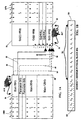
- FIG. 1A shows the physical layout of a representative boot memory array.
- FIG. 1B show the address bitlines for the representative boot memory array.
- the array is divided into five asymmetric contiguous blocks; a 16 Kb boot block 56, two 8 Kb parameter blocks, a 96 Kb main memory block and a 128 Kb main memory block 58.
- the blocks are physically asymmetric in terms of both block size and capability. Each of the blocks are individually erasable in bulk.
- the 16 Kb boot block can be locked to prevent overriding the kernel code that it contains for booting the computer.
- the 16Kb boot block 56 provides a secure storage area for the kernel code required to boot a system in the event of a power failure, or other disruption during code update.
- the boot sector is lockable, typically by means of an external pin on the memory chip, so that only under exceptional circumstances can the code contained therein be erased.
- the lock feature ensures absolute data integrity by preventing the boot block from being programmed, or erased when the external pin is not at a specific elevate voltage, e.g., 12 volt.
- the boot block can be erased and programmed when the block pin is held at 12 volt for the duration of the erase or program operation. This lock feature allows customers to change the boot code for upgrades while still providing security needed during normal operation.
- Each of the 8Kb parameter blocks provides storage for frequently updated system parameters and configuration or diagnostic information.
- the parameter blocks can also be used to store additional boot or main code.
- the parameter blocks do not have the hardware write protection feature, i.e., the lock feature that the boot block has.
- the 96Kb main memory block and the 128Kb main memory block 58 handle the remaining code.
- the physical block layout 40 is shown in both an upright 40-B and inverted 40-T physical memory map.
- the only distinguishing features between the upright and inverted form are the physical address locations at which the respective blocks are located.
- the boot block is either at the bottom of the physical memory map at address 00000h, or at the top of the memory map at adddress 3FFFFh.
- Address box 52 Tb shows the five most significant bits of the address associated with the T-type memory array layout 40-T.
- Address box 52 Bb shows the five most significant bits of the addresses associated with the B-type memory layout 40-B. Eighteen address bits are sufficient to address the five memory blocks which total 256 Kb of memory.
- the current invention provides an apparatus for allowing a single memory array to accommodate both T-type and B-type address protocols.
- the decoding that is implemented is either total or partial address decoding.
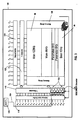
- Map lines 60-62 show the results of what will be identified as a total address decode on bits A 0 -A 17 .
- Map lines 64-66 corresponds to what will be identified as a partial decode of the five most significant bits of a memory access request address.
- FIG. 1B In order to better understand and appreciate the decoding, reference is made to FIG. 1B in which an 18 bit address A 0 -A 17 is shown.
- the eighteen bit address 80 is divided into a partial decode section 82 comprising address bits A 13 -A 17 . These bits are shown in binary form in boxes 52 Tb and 52 Bb.
- the remaining least significant bits 84 of the address are also shown in FIG. 1B . These are bits A 0 -A 12 .
- the total address decode is appropriate when an incoming boot block memory access request is accompanied by an address, which does not correspond to the physical location of the boot block in the memory array. Decoding is not necessary when an incoming boot block memory access does correspond to the physical location of the boot block in a memory array.
- the boot block In physical layout 40-B, the boot block is located between address 00000h and address 03FFFh. In the physical layout 40-T the boot block is located between address 3FFFFh and address 3C000h. If a microprocessor boot address corresponds to the actual location of the boot code in memory, then no address decoding is necessary. If the physical layout of the memory array does not initially correspond to address protocol of the microprocessor to which the memory chip utilizing this decoding, then decoding will be necessary. The decoding can be total or partial.
- Total decoding involves all eighteen bits 80 of a memory access request. Partial decoding involves only the most significant bits 82 of the memory access request.
- map lines 60-62 show the effect of total decoding of a memory access request from a microprocessor whose power-up boot address is address 00000h. That microprocessor is said to implement a B-type boot protocol because on power-up it looks to the bottom of the memory map for the kernal boot code.
- Map lines 60-62 show the decoding required to interface a B-type microprocessor to a boot chip in which the boot memory resides at the top of the memory map. Map line 60 corresponds to a boot memory access request at address of 00000h.
- Map line 62 shows that a memory access request to address 03FFFh will be decoded by performing a logical compliment on all bits of the address, the result of which is a conversion to address 3C000h which is the end of the boot block.
- total address decoding results in a complete inversion of the correlation between a memory access request and a physical memory address. Because the inversion is complete a linear traversal 68 of the entire 256 Kb of the inverted memory map results.
- partial address decoding of the most significant bits 82 of an incoming address may be appropriate. Partial address decoding requires a correlation between the minimum block size on the memory array, and the address range which the segment 84 of least significant bits will code for. When all blocks of memory are integer multiples of the minimum block size the number of bits in the segment 84 must map to the minimum segment size. In the example shown, the minimum block size is 8Kb, i.e., the size of the parameter blocks. Addresses A 0 -A 12 map to 8 Kb. Additionally, all blocks in the example shown are integer multiples of 8 Kb. Thus, segment 84 was chosen to have 13 bits which address 8Kb of memory. The remaining five most significant bits A 13 -A 17 are subject to partial decoding, which will be described shortly.
- segment size When the minimum memory block size is not evenly divisible into the block sizes of all remaining blocks, a smaller segment size must be chosen. That segment size must map to a byte size which is evenly divisible into all blocks sizes of the memory array including the smallest block.
- map lines 64-66 show an example of partial decoding. Partial decoding is not required when the boot address of the microprocessor and the physical address at which the boot code is located correspond. Partial decoding is appropriate when the microprocessor boot address and the physical address of boot block do not correspond.
- map lines 64-66 show the effect of partial decoding of a memory access request from a microprocessor whose power-up boot address is address 00000h. That microprocessor is said to implement a B-type boot protocol because on power-up it looks to the bottom of the memory map for the kernel boot code. Map lines 64-66 show an example of such partial decoding.
- a boot memory access request directed to address 00000h is partially decoded by logically complimenting the five most significant bits A 13 -A 17 of the incoming boot memory access request.
- the partially complimented/partially decoded address is 3E000h which lies in the bottom portion of the top half of the 16Kb boot block in the physical map 40-T.
- Map line 66 shows a memory access request directed to the end of the boot sector at address 03FFF, which is subject to partial decoding, i.e., complimenting of the five most significant bits.
- the decoding produces address 3DFFFh which maps to the top portion of the lower half of the 16Kb boot block 56 within T-type memory 40-T. The traversal of the memory array in this instance, i.e.
- partial decoding is non-linear in contrast to full decoding which exhibits linear traversal 68.
- the non-linear traversal 70 of the physical memory map is represented by hook and loop 70. From starting address 3E000h code which is laid out in block 56 in linear order is instead laid out in two discrete subblocks. The first sub-block begins at address 3E000h and ends at address 3FFFFh. The code continues at the beginning of the next subsegment at address 3C000h and proceeds to the end of that sub-block at address 3DFFFh.
- T-type microprocessors request boot code from the top of the memory map address 3FFFFh.
- the decoder setting should be off.
- a boot memory access request to which that memory will be subject is a B-type access request, i.e. requests from microprocessors which request a boot code to be found at address 00000h then decoding is necessary.
- Decoding can be either partial or total. In either case, decode settings must be enabled when a code is being written to the memory array in order for it to be placed in the appropriate sector and order.
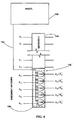
- FIG. 2 is an overall hardware block diagram of a computer utilizing a memory device which supports multiple address protocols.
- Microprocessor 100, main memory 106, boot memory 108 and address and data buffers respectively, 102-104 are shown.
- the microprocessor address output is connected via local address bus 126 to address buffer 102.
- Address buffer 102 is connected via system bus 124 to both main memory 106 and boot memory 108.
- the microprocessor data I/O is also connected via data bus 122 to data buffer 104.
- Data buffer 104 is connected via system bus 124 to both main memory 106 and boot memory 108.
- Boot memory 108 is non-volatile programmable memory which contains boot code for powering up the computer and all associated input and output (I/O) devices.
- the memory 108 may be flash memory, e.g., EEPROM, EPROM or ROM.
- the memory has an address protocol converter which causes the boot sector to appear to reside in either the upper or lower portion of logical memory depending on which of the two address protocols, B-type or T-type the microprocessor is implementing.
- boot code is uploaded from memory 108 and causes the processor to configure the surrounding hardware and I/O devices, i.e., keyboard, mouse, monitor, and main memory 106.
- FIG. 3 is a detailed hardware block diagram of flash memory 108 shown in FIG. 2 .
- the device includes a memory array 130 surrounded by X and Y decoders 120-118, Y-selector 122, output buffer 124, address input buffer 116, address protocol conversion logic 132 and address protocol control 136.
- the memory array 130 includes a 16 Kb lockable boot sector 56.
- the memory array also includes two 8 Kb parameter blocks, a 96Kb main memory block, and a 128Kb main memory block 58.
- the physical layout of the memory array corresponds to the physical structure 54 discussed above in FIG. 1 .
- the boot block 56 has circuitry for enforcing the write protection discussed above including an external locking pin.
- Each of the five blocks is individually erasable in bulk.
- the memory array has an asymmetric physical architecture.
- the data storage units for each cell of the memory array are floating gates. In a floating gate array, an individual transistor stores a logic 1/0 condition in the form of a high or low charge level on the floating gate portion of the floating gate transistor, which forms the memory component of each cell.
- the memory array 130 is oriented in rows and columns. Rows of the memory array are connected to the X-decoder 120. A portion of the X-decoder 120 includes an address protocol conversion unit 132. In the example shown, the five most significant bits of the address input contain the address protocol conversion unit 132 of the current invention. This unit implements partial address decoding. This unit has circuitry which implements an XOR function on each of address lines A 13 -A 17 . One input of each XOR logic unit is connected to a signal line 134 from the address protocol controller 136. The remaining input of each logic unit is connected to a corresponding one of address input lines A 13 -A 17 . The columns of the memory array are connected to the Y-selector 122.
- the Y-selector performs both as a sense amp and as a column selector, under the control of Y-decoder 118. Both the X and Y decoders are connected to address input buffer 116. The Y-selector/sense amp 122 is connected to output buffer 124.
- an address on lines A 0 -A 17 is stored in address input buffer 116.
- the addresses stored in the address input buffer are supplied to the X and Y decoders 120-118 respectively.
- the address protocol conversion unit 132 will complement each of the address inputs A 13 -A 17 if an address complement signal is present on signal line 134.
- the output of the X-decoder selects a specific row in memory array 130 to be read from or written to.
- the specific column(s) of the selected row are selected via Y-decoder 118 operating in conjunction with Y-selector/sense amp 122.
- the charge on the transistor of the individual cells within the selected column and row is determined by Y-selector/sense amp 122 and stored in output buffer 124 as binary "1/0".
- Each of the output buffers O 0 -O 15 is connected to the system bus 124 to read/write data from/to the memory array.
- Each of the five blocks of the memory array 130 can be individually erased in bulk.
- Boot block 56 contains the kernel code for booting the system.
- the 16 Kb sector of the memory array which contains this code can be lock protected as discussed above.
- FIG. 4 is a detailed view of the X-decoder 120, the address protocol conversion unit 132 and the address protocol control 136.
- Exclusive Or (XOR) gates 132A-E are shown with an input of each gate connected to a corresponding one of address lines A 13 - 17 .
- Each of the remaining inputs of the XOR gates are connected in parallel via signal line 134 to address protocol control unit 136.
- a signal output by address protocol control unit 136 on signal line 134 will have a logic 1 or 0 level.
- the output of each of gates 132A-E will be identical to the input on each of address lines A 13 - 17 .
- the addresses present at the output of each of XOR gates 132A-E will be the logical complement of respectively address input lines A 13 - 17 .
- the partial address decoding circuit shown in FIG. 4 allows a memory array having either a B-type or T-type physical layout to accept inputs from processors implementing either a B-type or T-type protocol. For example, if the memory array is laid out at a physical level with a T-type structure then the 16Kb boot block will be located at physical address 3COOOh->3FFFFh. In this case, addresses received from a processor implementing a T-type protocol will not be converted/complemented and therefore address protocol control unit 136 will output a logic 0 level signal. Thus, the output of each of gates 132A-E will be identical to the address A 13 - 17 inputs.
- each of address inputs A 13 - 17 will be complemented in order to redirect memory accesses, i.e., read/write to the appropriate memory block.
- the "GoTo on Boot" address for a B-Type processor is 00000h. After protocol conversion this address is 3E000h which is the bottom portion of the upper half of the 16Kb boot block 56.
- Exclusive Nor (XNOR) logic can also be used to implement the same features discussed above, by reversing the signal logic on signal line 134.
- the address protocol conversion unit 132 can be implemented on any number of address lines without departing from the teachings of this invention.
- the address protocol conversion unit may also be utilized in memory arrays which do provide symmetrical block sizes and block array features.
- the address complementation circuitry may be implemented in any memory array including volatile and non-volatile memory, e.g., DRAM, SRAM, EPROM, EEPROM in which it is advantageous to have the capability to complement one or more incoming address lines.
- total address conversion can be implemented by adding an XOR or XNOR gate to all address inputs.
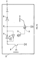
- FIGS. 5A-B show alternate embodiments of the detailed circuitry connected with the address protocol control 136.
- FIG. 5A shows the first of those embodiments of address protocol control 136A.
- a transistor 154, a floating gate transistor 162 and inverters 150-152, 156 are shown.
- the source of floating gate transistor 162 is connected to ground.
- the gate of floating gate transistor 162 is connected to program voltage source 158.
- the drain of floating gate transistor 162 is connected to a node common to the input of inverter 152 and the "output" of a back-to-back inverter pair 150, 156 and specifically the output of inverter 150 and the input of inverter 156.
- the "input" of the inverter pair 150, 156 and specifically the input of inverter 150 and the output of inverter 156 is connected to the drain of transistor 154.
- the source of transistor 154 is connected to ground.
- the gate of transistor 154 is connected to an initialization signal line.
- the signal present on signal line 134 is determined by the amount of charge (Q) on the floating gate of floating gate transistor 162.
- Q the amount of charge
- a logic "0" voltage level on signal line 134 results from a relatively high charge amount Q, while a logic “1” on signal line 134 results from a relatively low charge amount Q.
- a signal VDD would be present on the gate of transistor 154.
- the input of inverter 150 will be shorted to ground, and therefore the signal level at node 160 will be VDD.
- the signal present on the gate of transistor 154 returns to ground level.
- the input to inverter 150 is floating at a voltage level determined by the amount of feedback provided by weak inverter 156.
- the signal level on node 160 depends on the voltage level on the floating gate of floating transistor 162.
- the gate of floating gate transistor 162 is supplied with voltage level VDD by voltage source 158. If a "low threshold" charge, i.e., low charge amount, is present on the gate of that transistor, transistor 162 will sink the limited current provided by inverter 150 to ground. This will cause node 160 to drop to a low voltage level.
- the low voltage level on node 160 will be reinforced by feedback from inverter 156 the output of which will force the input of inverter 150 to a high voltage level. This in turn will lock the output of inverter 150, i.e. node 160 at ground.
- the low voltage at node 160 will be inverted by inverter 152, thereby producing a logic level "1" on signal line 134.
- the charge level present on the floating gate of floating gate transistor 162 can be programmed via voltage source 158.
- the program voltage on the gate of transistor 162 can be varied via a dedicated external pin, or by a unique combination of signals on existing pins which cause on chip logic to supply both a program voltage, i.e. VDD++ or VSS--, and an operational voltage VDD.
- a high voltage level VDD++ provided by voltage source 158 to the gate of the floating gate transistor in conjunction with a voltage level VDD on node 160 can be used to program a "high threshold" state on transistor 162, resulting from a relatively high charge level.
- a negative voltage level provided by voltage source 158 can be used to remove charge from gate of floating gate transistor 162 thereby creating a "low threshold" condition, resulting from a relatively low charge level Q.
- This bit level programming can be implemented without affecting the manufacturing process for the chip.
- a single chip can be utilized with either B-type or T-type logical address protocols.
- Address protocol control 136B includes a single pole double throw (SPDT) switch 164.
- SPDT single pole double throw
- the output of the switch is connected to signal line 134 [see FIG. 4 ].
- the input of the switch can be connected either to VDD or ground.
- the switch can be implemented as a fusible link connected to an internal voltage source at either a VDD or ground level. Alternately, the switch can be implemented as a single external pin/jumper connected to either a high or low voltage level depending on the address protocol being implemented.
- FIG. 6 shows an embodiment of the address protocol conversion unit 132 [see FIG. 4 ].
- CMOS Circuitry for implementing the XOR function is shown.
- the circuitry for a representative gate 132A includes inverters 202 and 206 and back-to-back pairings of p-type and n-type pass transistors 200, 204 and 208-210.
- Transistors 200 and 208 are n-type devices.
- Transistors 204 and 210 are p-type devices.
- the drains of each of transistor pairs 200, 204 and 208-210 provide the output of the gate.
- the inputs, i.e. the sources of each of the transistor pairs 200, 204 and 208-210 are connected to respectively the output of inverter 202 and to address A 13 input line.
- inverter 202 is also connected to address A 13 input.
- the sources of transistors 208-210 are connected directly to the address A 13 input line while the sources of transistors 200, 204 are connected to the inverted signal from input line A 13 .
- the gates of transistors 200 and 210 are connected directly to signal line 134.
- Signal line 134 is connected to the address protocol control 136 [see FIG. 4 ].
- the gates of transistors 204 and 208 are connected to the output of inverter 206.
- the input of inverter 206 is also connected to signal line 134.
- both transistors 200 and 204 are in an open circuit condition while transistors 208 and 210 are in a closed circuit condition.
- the output signal is identical to the logic level on address line on A 13 .
- both transistors 208 and 210 are in an open circuit condition while transistors 200 and 204 are in a closed circuit condition.
- the address output is the complement of the address input on signal line A 13 .
Landscapes
- Engineering & Computer Science (AREA)
- Software Systems (AREA)
- Theoretical Computer Science (AREA)
- Microelectronics & Electronic Packaging (AREA)
- Computer Security & Cryptography (AREA)
- Physics & Mathematics (AREA)
- General Engineering & Computer Science (AREA)
- General Physics & Mathematics (AREA)
- Read Only Memory (AREA)
Claims (12)
- Halbleiterspeichervorrichtung, die aufweist:ein Speicher-Array (130) mit Zeilen und Spalten von Speicherzellen,einen ersten Block (56), der einen Satz von Zeilen aus dem Speicher-Array (130) zum Speichern von Daten beinhaltet, die entweder im oberen oder im unteren Teil des physikalischen Speicherplans des Speicher-Arrays (130) liegen, undDecoder (118, 120) für eine Speicherzugriffsanforderung für die Daten in dem ersten Block (56), wobei die Speicherzugriffsanforderung sich entweder in einem Adreßprotokoll eines ersten Typs, bei dem Adressen für das Zugreifen auf den ersten Block (56) Adreßbits höherer Ordnung beinhalten, an den oberen Teil des physikalischen Speicherplans des Speicher-Arrays (130) richtet, oder in einem Adreßprotokoll eines zweiten Typs, bei dem Adressen für das Zugreifen auf den ersten Block (56) Adreßbits höherer Ordnung beinhalten, an den unteren Teil des physikalischen Speicherplans des Speicher-Arrays (130) richtet, und die Decoder (118, 120) eine Logik (132) beinhalten, um die Adreßbits höherer Ordnung in Reaktion auf das Vorliegen eines Adreßkomplementsignals auf einer Signalleitung (134) zu invertieren und Ausgangssignale auszugeben für das Auswählen einer Zeile des Speicher-Arrays in dem ersten Block in Reaktion auf die Speicherzugriffsanforderung entweder in dem Adreßprotokoll des ersten Typs oder in dem Adreßprotokoll des zweiten Typs, wobei das Adreßkomplementsignal auf der Signalleitung (134) anzeigt, daß die Speicherzugriffsanforderung von einer Adresse begleitet ist, die nicht der physikalischen Position des ersten Blocks in dem Speicher-Array (130) entspricht.
- Halbleiterspeichervorrichtung nach Anspruch 1, wobei die Logik (132) aufweist.
wenigstens ein Logikgate (132A) mit einem ersten Eingang, einem zweiten Eingang und einem Ausgang, und wobei das wenigstens eine Logikgate (132A) an dem ersten Eingang auf die Signalleitung (134) und an dem zweiten Eingang auf ein korrespondierendes Bit (A13) der Speicherzugriffsanforderung so reagiert, daß es in Reaktion auf einen ersten Zustand der Signalleitung (134) ein Ausgangssignal ausgibt, bei dem das korrespondierende Bit (A13) logisch invertiert ist, und in Reaktion auf einen zweiten Zustand der Signalleitung (134) ein Ausgangssignal ohne logische Invertierung des korrespondierenden Bits (A13) der Speicherzugriffsanforderung ausgibt. - Halbleiterspeichervorrichtung nach Anspruch 2, wobei das wenigstens eine Logikgate (132A) eine XOR-Logik aufweist und das Ausgangssignal als logisches "Ausschluß-Oder" des ersten Eingangs und des zweiten Eingangs ausgibt.
- Halbleiterspeichervorrichtung nach Anspruch 2, wobei das wenigstens eine Logikgate (132A) eine XNOR-Logik aufweist und das Ausgangssignal als logisches "Ausschluß-Nicht-Oder" des ersten Eingangs und des zweiten Eingangs ausgibt.
- Halbleiterspeichervorrichtung nach Anspruch 2, die weiterhin eine Adreßprotokollsteuerung (136) aufweist, die mit der Signalleitung (134) verbunden ist und eine Brückenverbindung beinhaltet und auf einen Anschluß an eine Spannung VDD so reagiert, daß sie auf der Signalleitung (134) ein Signal ausgibt, welches entweder das Adreßprotokoll des ersten Typs oder das Adreßprotokoll des zweiten Typs anzeigt, und auf einen Anschluß an eine Spannung VSS so reagiert, daß sie auf der Signalleitung (134) ein Signal ausgibt, welches ein anderes des ersten Typs oder des zweiten Typs des Adreßprotokolls anzeigt.
- Halbleiterspeichervorrichtung nach Anspruch 2, die weiterhin eine Adreßprotokollsteuerung (136) aufweist, die mit der Signalleitung (134) verbunden ist und einen Schmelzeinsatz beinhaltet, der abschmelzbar mit einer Spannung VDD verbindbar ist, um auf der Signalleitung (134) ein Signal auszugeben, welches entweder das Adreßprotokoll des ersten Typs oder das Adreßprotokoll des zweiten Typs anzeigt und abschmelzbar mit einer Spannung VSS verbindbar ist, um auf der Signalleitung (134) ein Signal auszugeben, welches einen anderen des ersten Typs oder des zweiten Typs des Adreßprotokolls anzeigt.
- Halbleiterspeichervorrichtung nach Anspruch 2, die weiterhin eine Adreßprotokollsteuerung (136) beinhaltet, die mit der Signalleitung (134) verbunden ist und aufweist:einen Schalter mit einer programmierbaren Floating-Gate-Speicherzelle (162) mit einem Steuergate, einem potentialfreien Gate, einer Quelle und einer Senke, und das Steuergate ist mit einer ersten Spannungsversorgung verbunden, die Senke ist mit einer zweiten Spannungsversorgung verbunden, und ein Niveau der ersten Spannungsversorgung ist ausreichend, um die Quelle mit der zweiten Spannungsversorgung zu verbinden, wenn das potentialfreie Gate mit einer "niedrigen Schwellwert"-Ladung programmiert ist, um so auf der Signalleitung (134) ein Signal zu erzeugen, welches das Adreßprotokoll des ersten Typs anzeigt, und das Niveau der ersten Spannungsversorgung ist ausreichend, um die Quelle von der Senke zu trennen, wenn das potentialfreie Gate mit einer "hohen Schwellwert"-Ladung programmiert ist, um so auf der Signalleitung (134) ein Signal zu erzeugen, welches das Adreßprotokoll des zweiten Typs anzeigt.
- Halbleiterspeichervorrichtung nach Anspruch 2,
wobei die in dem ersten Block (56) gespeicherten Daten Boot-Code für das Konfigurieren eines Computers für das Hochfahren enthalten. - Halbleiterspeichervorrichtung nach Anspruch 1, wobei weiterhin
der erste Block (56) eine Zwischenspeichermöglichkeit beinhaltet, um zu verhindern, daß die gespeicherten Daten, einschließlich darin enthaltenem Boot-Code für das Konfigurieren eines Computers, gelöscht werden. - Halbleiterspeichervorrichtung nach Anspruch 1, wobei weiterhin
die in dem ersten Block gespeicherten Daten Boot-Code für das Reagieren auf eine Speicherzugriffsanforderung nach Boot-Code enthalten, um einen Computer für das Hochfahren zu konfigurieren. - Halbleiterspeichervorrichtung nach Anspruch 1, wobei weiterhin
das Speicher-Array (130) in wenigstens den ersten Block (56) und einen zweiten Block unterteilt ist und die Anzahl der Zeilen in dem ersten Block nicht gleich der Anzahl der Zeilen in dem zweiten Block ist. - Halbleiterspeichervorrichtung nach Anspruch 10, wobei die Logik (132) aufweist:einen gesteuerten Inverter (200-210), um eine Gruppe von Adreßbits der Speicherzugriffsanforderung, beginnend bei einem höchstwertigen Bit, zu invertieren, um die Speicherzugriffsanforderung an den ersten Block (56) zu decodieren.
Applications Claiming Priority (1)
| Application Number | Priority Date | Filing Date | Title |
|---|---|---|---|
| PCT/US1998/000459 WO1999035649A1 (en) | 1998-01-06 | 1998-01-06 | A memory supporting multiple address protocols |
Publications (3)
| Publication Number | Publication Date |
|---|---|
| EP1058930A1 EP1058930A1 (de) | 2000-12-13 |
| EP1058930A4 EP1058930A4 (de) | 2005-02-16 |
| EP1058930B1 true EP1058930B1 (de) | 2009-06-03 |
Family
ID=22266182
Family Applications (1)
| Application Number | Title | Priority Date | Filing Date |
|---|---|---|---|
| EP98901220A Expired - Lifetime EP1058930B1 (de) | 1998-01-06 | 1998-01-06 | Ein multipeladdressenprotokoll unterstützender speicher |
Country Status (4)
| Country | Link |
|---|---|
| EP (1) | EP1058930B1 (de) |
| JP (1) | JP2002501275A (de) |
| DE (1) | DE69840877D1 (de) |
| WO (1) | WO1999035649A1 (de) |
Families Citing this family (4)
| Publication number | Priority date | Publication date | Assignee | Title |
|---|---|---|---|---|
| US6058463A (en) * | 1998-01-20 | 2000-05-02 | Motorola, Inc. | Paged memory data processing system with overlaid memory control registers |
| US6407949B1 (en) * | 1999-12-17 | 2002-06-18 | Qualcomm, Incorporated | Mobile communication device having integrated embedded flash and SRAM memory |
| JP4731020B2 (ja) * | 2001-01-24 | 2011-07-20 | 富士通セミコンダクター株式会社 | 半導体記憶装置、セクタアドレス変換回路、アドレス変換方法及び半導体記憶装置の使用方法 |
| US7813212B2 (en) | 2008-01-17 | 2010-10-12 | Mosaid Technologies Incorporated | Nonvolatile memory having non-power of two memory capacity |
Family Cites Families (5)
| Publication number | Priority date | Publication date | Assignee | Title |
|---|---|---|---|---|
| IT1254937B (it) * | 1991-05-06 | 1995-10-11 | Aggiornamento dinamico di memoria non volatile in un sistema informatico | |
| US5245572A (en) * | 1991-07-30 | 1993-09-14 | Intel Corporation | Floating gate nonvolatile memory with reading while writing capability |
| US5473775A (en) * | 1991-10-11 | 1995-12-05 | Kabushiki Kaisha Toshiba | Personal computer using flash memory as BIOS-ROM |
| JPH06119230A (ja) * | 1992-10-06 | 1994-04-28 | Fujitsu Ltd | 半導体記憶装置 |
| US5680556A (en) * | 1993-11-12 | 1997-10-21 | International Business Machines Corporation | Computer system and method of operation thereof wherein a BIOS ROM can be selectively locatable on diffeent buses |
-
1998
- 1998-01-06 EP EP98901220A patent/EP1058930B1/de not_active Expired - Lifetime
- 1998-01-06 DE DE69840877T patent/DE69840877D1/de not_active Expired - Lifetime
- 1998-01-06 WO PCT/US1998/000459 patent/WO1999035649A1/en active Application Filing
- 1998-01-06 JP JP2000527945A patent/JP2002501275A/ja active Pending
Also Published As
| Publication number | Publication date |
|---|---|
| EP1058930A1 (de) | 2000-12-13 |
| JP2002501275A (ja) | 2002-01-15 |
| DE69840877D1 (en) | 2009-07-16 |
| WO1999035649A1 (en) | 1999-07-15 |
| EP1058930A4 (de) | 2005-02-16 |
Similar Documents
| Publication | Publication Date | Title |
|---|---|---|
| US5245572A (en) | Floating gate nonvolatile memory with reading while writing capability | |
| US6119226A (en) | Memory supporting multiple address protocols | |
| CN102543169B (zh) | 统一的多级单元存储器 | |
| US5999441A (en) | Random access memory having bit selectable mask for memory writes | |
| CN100520974C (zh) | 带由分离读写信号驱动逻辑行解码器电路的边读边写闪存 | |
| US7707368B2 (en) | Memory device trims | |
| US5046046A (en) | Redundancy CAM using word line from memory | |
| US5732207A (en) | Microprocessor having single poly-silicon EPROM memory for programmably controlling optional features | |
| US5280447A (en) | Floating gate nonvolatile memory with configurable erasure blocks | |
| US5574688A (en) | Apparatus and method for mapping a redundant memory column to a defective memory column | |
| US5572470A (en) | Apparatus and method for mapping a redundant memory column to a defective memory column | |
| US5047989A (en) | Chapter mode selection apparatus for MOS memory | |
| JPH0157438B2 (de) | ||
| US6950336B2 (en) | Method and apparatus for emulating an electrically erasable programmable read only memory (EEPROM) using non-volatile floating gate memory cells | |
| EP0905704B1 (de) | Sektorbasierter Halbleiterspeicher mit verstellbaren Sektoradressen | |
| US20060239074A1 (en) | Using redundant memory for extra features | |
| EP1058930B1 (de) | Ein multipeladdressenprotokoll unterstützender speicher | |
| US6400611B1 (en) | Independent asynchronous boot block for synchronous non-volatile memory devices | |
| US6549468B2 (en) | Non-volatile memory with address descrambling | |
| US6075721A (en) | Random access memory having bit selectable mask for memory writes | |
| US20060250845A1 (en) | Layout for NAND flash memory array having reduced word line impedance | |
| US7551481B2 (en) | User configurable commands for flash memory | |
| JPS5931744B2 (ja) | Mosデジタルコンピユ−タ | |
| US4875191A (en) | Integrated read and programming row driver | |
| US6643174B2 (en) | EEPROM cells and array with reduced write disturbance |
Legal Events
| Date | Code | Title | Description |
|---|---|---|---|
| PUAI | Public reference made under article 153(3) epc to a published international application that has entered the european phase |
Free format text: ORIGINAL CODE: 0009012 |
|
| 17P | Request for examination filed |
Effective date: 20000713 |
|
| AK | Designated contracting states |
Kind code of ref document: A1 Designated state(s): DE FR GB |
|
| RAP1 | Party data changed (applicant data changed or rights of an application transferred) |
Owner name: MACRONIX INTERNATIONAL CO., LTD. |
|
| A4 | Supplementary search report drawn up and despatched |
Effective date: 20050105 |
|
| GRAP | Despatch of communication of intention to grant a patent |
Free format text: ORIGINAL CODE: EPIDOSNIGR1 |
|
| RIC1 | Information provided on ipc code assigned before grant |
Ipc: G06F 9/445 20060101ALN20080827BHEP Ipc: G11C 8/00 20060101AFI20080827BHEP |
|
| GRAS | Grant fee paid |
Free format text: ORIGINAL CODE: EPIDOSNIGR3 |
|
| GRAA | (expected) grant |
Free format text: ORIGINAL CODE: 0009210 |
|
| AK | Designated contracting states |
Kind code of ref document: B1 Designated state(s): DE FR GB |
|
| REG | Reference to a national code |
Ref country code: GB Ref legal event code: FG4D |
|
| REF | Corresponds to: |
Ref document number: 69840877 Country of ref document: DE Date of ref document: 20090716 Kind code of ref document: P |
|
| PLBE | No opposition filed within time limit |
Free format text: ORIGINAL CODE: 0009261 |
|
| STAA | Information on the status of an ep patent application or granted ep patent |
Free format text: STATUS: NO OPPOSITION FILED WITHIN TIME LIMIT |
|
| 26N | No opposition filed |
Effective date: 20100304 |
|
| REG | Reference to a national code |
Ref country code: FR Ref legal event code: PLFP Year of fee payment: 19 |
|
| REG | Reference to a national code |
Ref country code: FR Ref legal event code: PLFP Year of fee payment: 20 |
|
| PGFP | Annual fee paid to national office [announced via postgrant information from national office to epo] |
Ref country code: FR Payment date: 20170104 Year of fee payment: 20 Ref country code: DE Payment date: 20170104 Year of fee payment: 20 |
|
| PGFP | Annual fee paid to national office [announced via postgrant information from national office to epo] |
Ref country code: GB Payment date: 20170104 Year of fee payment: 20 |
|
| REG | Reference to a national code |
Ref country code: DE Ref legal event code: R071 Ref document number: 69840877 Country of ref document: DE |
|
| REG | Reference to a national code |
Ref country code: GB Ref legal event code: PE20 Expiry date: 20180105 |
|
| PG25 | Lapsed in a contracting state [announced via postgrant information from national office to epo] |
Ref country code: GB Free format text: LAPSE BECAUSE OF EXPIRATION OF PROTECTION Effective date: 20180105 |