EP1058195A2 - Réseau logique minimal à niveaux multiples - Google Patents
Réseau logique minimal à niveaux multiples Download PDFInfo
- Publication number
- EP1058195A2 EP1058195A2 EP00120188A EP00120188A EP1058195A2 EP 1058195 A2 EP1058195 A2 EP 1058195A2 EP 00120188 A EP00120188 A EP 00120188A EP 00120188 A EP00120188 A EP 00120188A EP 1058195 A2 EP1058195 A2 EP 1058195A2
- Authority
- EP
- European Patent Office
- Prior art keywords
- node
- data
- nodes
- message
- interconnect
- Prior art date
- Legal status (The legal status is an assumption and is not a legal conclusion. Google has not performed a legal analysis and makes no representation as to the accuracy of the status listed.)
- Withdrawn
Links
Images


Classifications
-
- G—PHYSICS
- G06—COMPUTING; CALCULATING OR COUNTING
- G06F—ELECTRIC DIGITAL DATA PROCESSING
- G06F15/00—Digital computers in general; Data processing equipment in general
- G06F15/16—Combinations of two or more digital computers each having at least an arithmetic unit, a program unit and a register, e.g. for a simultaneous processing of several programs
- G06F15/163—Interprocessor communication
- G06F15/173—Interprocessor communication using an interconnection network, e.g. matrix, shuffle, pyramid, star, snowflake
- G06F15/17356—Indirect interconnection networks
- G06F15/17368—Indirect interconnection networks non hierarchical topologies
- G06F15/17393—Indirect interconnection networks non hierarchical topologies having multistage networks, e.g. broadcasting scattering, gathering, hot spot contention, combining/decombining
-
- G—PHYSICS
- G06—COMPUTING; CALCULATING OR COUNTING
- G06F—ELECTRIC DIGITAL DATA PROCESSING
- G06F15/00—Digital computers in general; Data processing equipment in general
- G06F15/16—Combinations of two or more digital computers each having at least an arithmetic unit, a program unit and a register, e.g. for a simultaneous processing of several programs
- G06F15/163—Interprocessor communication
- G06F15/173—Interprocessor communication using an interconnection network, e.g. matrix, shuffle, pyramid, star, snowflake
- G06F15/17356—Indirect interconnection networks
- G06F15/17368—Indirect interconnection networks non hierarchical topologies
- G06F15/17375—One dimensional, e.g. linear array, ring
-
- G—PHYSICS
- G06—COMPUTING; CALCULATING OR COUNTING
- G06F—ELECTRIC DIGITAL DATA PROCESSING
- G06F15/00—Digital computers in general; Data processing equipment in general
- G06F15/76—Architectures of general purpose stored program computers
- G06F15/80—Architectures of general purpose stored program computers comprising an array of processing units with common control, e.g. single instruction multiple data processors
- G06F15/8007—Architectures of general purpose stored program computers comprising an array of processing units with common control, e.g. single instruction multiple data processors single instruction multiple data [SIMD] multiprocessors
- G06F15/803—Three-dimensional arrays or hypercubes
-
- H—ELECTRICITY
- H04—ELECTRIC COMMUNICATION TECHNIQUE
- H04L—TRANSMISSION OF DIGITAL INFORMATION, e.g. TELEGRAPHIC COMMUNICATION
- H04L12/00—Data switching networks
- H04L12/28—Data switching networks characterised by path configuration, e.g. LAN [Local Area Networks] or WAN [Wide Area Networks]
- H04L12/42—Loop networks
-
- H—ELECTRICITY
- H04—ELECTRIC COMMUNICATION TECHNIQUE
- H04L—TRANSMISSION OF DIGITAL INFORMATION, e.g. TELEGRAPHIC COMMUNICATION
- H04L45/00—Routing or path finding of packets in data switching networks
- H04L45/02—Topology update or discovery
- H04L45/06—Deflection routing, e.g. hot-potato routing
Definitions
- the present invention relates to interconnection structures for computing and communication systems. More specifically, the present invention relates to multiple level interconnection structures in which control and logic circuits are minimized.
- One technique for interconnecting parallel computational units involves construction of a communication network similar to a telephone network in which groups of network elements are connected to switching systems.
- the switching systems are interconnected in a hierarchical manner so that any switching station manages a workable number of connections.
- One disadvantage of a network connection is an increase in the latency of access to another computational unit since transmission of a message traverses several stages of a network. Typically, periods of peak activity occur in which the network is saturated with numerous messages so that many messages simultaneously contend for the use of a switching station.
- Various network types have been devised with goals of reducing congestion, improving transmission speed and achieving a reasonable cost. These goals are typically attained by rapidly communicating between nodes and minimizing the number of interconnections that a node must support.
- One conventional interconnection scheme is a ring of nodes with each node connected to two other nodes so that the line of interconnections forms a circle.
- the definition of a ring in accordance with a standard definition of a ring network in the art of computing ( IBM Dictionary of Computing , McDaniel G. ed., McGraw-Hill, Inc., 1994, p. 584) is a network configuration in which devices are connected by unidirectional transmission links to form a closed path.
- Another simple conventional scheme is a mesh in which each node is connected to its four nearest neighbors. The ring and mesh techniques advantageously limit the number of interconnections supported by a node.
- the ring and mesh networks typically are plagued by lengthy delays in message communication since the number of nodes traversed in sending a message from one node to another may be quite large. These lengthy delays commonly cause a computational unit to remain idle awaiting a message in transit to the unit.
- the earliest networks generally beginning with telephone networks, utilize circuit switching in which each message is routed through the network along a dedicated path that is reserved for the duration of the communication analogous to a direct connection via a single circuit between the communicating parties.
- Circuit switching disadvantageously requires a lengthy setup time. Such delays are intolerable during the short and quick exchanges that take place between different computational units.
- a dedicated pathway is very wasteful of system bandwidth.
- One technique for solving the problems arising using circuit switching is called packet switching in which messages sent from one computational unit to another does not travel in a continuous stream to a dedicated circuit. Instead, each computational unit is connected to a node that subdivides messages into a sequence of data packets.
- a message contains an arbitrary sequence of binary digits that are preceded by addressing information.
- the length of the entire message is limited to a defined maximum length.
- a "header" containing at least the destination address and a sequence number is attached to each packet, and the packets are sent across the network. Addresses are read and packets are delivered within a fraction of a second. No circuit setup delay is imposed because no circuit is set up. System bandwidth is not wasted since there is no individual connection between two computational units. However, a small portion of the communication capacity is used for routing information, headers and other control information. When communication advances in isolated, short bursts, packet switching more efficiently utilizes network capacity. Because no transmission capacity is specifically reserved for an individual computational unit, time gaps between packets are filled with packets from other users. Packet switching implements a type of distributed multiplexing system by enabling all users to share lines on the network continuously.
- a multiple level minimum logic network interconnect structure has a very high bandwidth and low latency. Control of interconnect structure switching is distributed throughout multiple nodes in the structure so that a supervisory controller providing a global control function is not necessary. A global control function is eliminated and complex logic structures are avoided by a novel data flow technique that is based on timing and positioning of messages communicating through the interconnect structure. Furthermore, the interconnect structure implements a "deflection" or "hot potato" design in which processing and storage overhead at each node is minimized by routing a message packet through an additional output port rather than holding the packet until a desired output port is available. Accordingly, the usage of buffers at the nodes is eliminated.
- Implementation of the interconnect structure is highly flexible so that fully electronic, fully optical and mixed electronic-optical embodiments are achieved. An implementation using all optical switches is facilitated by nodes exploiting uniquely simple logic and elimination of buffering at the nodes.
- the multiple level minimum logic network interconnect architecture is used for various purposes.
- the architecture is used as an interconnect structure for a massively parallel computer such as a supercomputer.
- the architecture forms an interconnect structure linking a group of workstations, computers, terminals, ATM machines, elements of a national flight control system and the like.
- Another usage is an interconnect structure in various telecommunications applications or an interconnect structure for numerous schedulers operating in a business main frame.
- an interconnect apparatus includes a plurality of nodes and a plurality of interconnect lines selectively connecting the nodes in a multiple level structure in which the levels include a richly interconnected collection of rings.
- the multiple level structure includes a plurality of J+1 levels in a hierarchy of levels and a plurality of 2 J K nodes at each level. If integer K is an odd number, the nodes on a level M are situated on 2 J-M rings with each ring including 2 M K nodes.
- Message data leaves the interconnect structure from nodes on a level zero.
- Each node has multiple communication terminals. Some are message data input and output terminals. Others are control input and output terminals.
- a node A on level 0 receives message data from a node B on level 0 and also receives message data from a node C on level 1.
- Node A sends message data to a node D on level 0 and also sends message data to a device E that is typically outside the interconnect structure.
- a device E is an input buffer of a computational unit.
- Node A receives a control input signal from a device F which is commonly outside the interconnect structure.
- An example of a device F is an output buffer of a computational unit.
- Node A sends a control signal to a node G on level 1.
- a node A on level J receives message data from a node B on level J and also receives message data from a device C that is outside the interconnect structure.
- device C is an output buffer of a computational unit.
- Node A sends message data to a node D on level J and also sends message data to a node E on level J-1.
- Node A receives a control input signal from a node F on level J-1.
- Node A sends a control signal to a device G that is typically outside the interconnect structure.
- An example of a device G is an output buffer of a computational unit.
- Nodes between the innermost level 0 and the outermost level J communicate message data and control signals among other nodes.
- a node A on a level T that is neither level 0 or level J receives message data from a node B on level T and also receives message data from a node C on level T + 1.
- Node A sends message data to a node D on level T and also sends message data to a node E on level T-1.
- Node A receives a control input signal from a node F on level T-1.
- Node A sends a control signal to a node G on level T+1.
- Level M has 2 J-M rings, each containing 2 M K nodes for a total of 2 J K nodes on level M. Specifically:
- a ring R T on a level T which is not the outermost level J For a ring R T on a level T which is not the outermost level J, then one ring R T+1 on level T+1 exists such tat each node A on ring R T receives data from a node B on ring R T and a node C on ring R T+1 .
- a ring R T on a level T which is not the innermost level 0 then there exist exactly two rings R1 T-1 and R2 T-1 on level T-1 such that a node A on ring R T sends message data to a node D on ring R T and a node E on either ring R1 T-1 or ring R2 T-1 .
- a message on any level M of the interconnect structure can travel to two of the rings on level M-1 and is eventually able to travel to 2 M of the rings on level 0.
- a "predecessor" of a node sends message data to that node.
- An “immediate predecessor” sends message data to a node on the same ring.
- a “successor” of a node receives message data from tat node.
- An “immediate successor” receives message data to a node on the same ring.
- node A RT on ring R T on level T there are nodes B RT and D RT on ring R T of level T such that node B RT is an immediate predecessor of node A RT and node D RT is an immediate successor of node A RT .
- Node A RT receives message data from node B RT and sends message data to node D RT .
- Node A RT receives message data from a device C that is not on the ring R T and sends data to a device E that is not on ring R T . If the level is not the innermost level 0, then device E is a node on level T-1 and there is an immediate predecessor node F on the same ring as device E.
- Node A RT receives control information from device F. If node A RT is on node T equal to zero, then device E is outside the interconnect structure and device E sends control information to node A RT . For example, if device E is an input buffer of a computational unit, then the control information from device E to node A RT indicates to node A RT whether device E is ready to receive message data from node A RT . Node D RT receives message data from a device G that is not on ring R T . Node A RT sends a control signal to device G.
- Control information is conveyed to resolve data transmission conflicts in the interconnect structure.
- Each node is a successor to a node on the adjacent outer level and an immediate successor to a node on the same level. Message data from the immediate successor nas priority.
- Control information is send from nodes on a level to nodes on the adjacent outer level to warn of impending conflicts.
- the interconnect structure forms a three-dimensional cylindrical structure.
- the interconnect structure is fully defined by designating the interconnections for each node A of each level T to devices or nodes B, C, D, E, F and G.
- Each node or device has a location designated in three-dimensional cylindrical coordinates (r, ⁇ , z) where radius r is an integer which specifies the cylinder number from 0 to J, angle ⁇ is an integer multiple of 2 ⁇ /K, which specifies the spacing of nodes around the circular cross-section of a cylinder from 0 to K-1, and height z is a binary integer which specifies distance along the z-axis from 0 to 2 J -1.
- Height z is expressed as a binary number because the interconnection between nodes in the z-dimension is most easily described as a binary digit manipulation.
- one ring is spanned in one pass through the angles ⁇ from 0 to K-1 and each height z designates a ring.
- one ring is spanned in two passes through the angles ⁇ and two heights z are used to designate one ring.
- the ring structure proceeds in this manner through the outermost ring J in which one ring is spanned in all 2 J heights along the z-axis.
- Node A on a ring R receives message data from a node B, which is an immediate predecessor of node A on ring R.
- node B For a node A located at a node position N(r, ⁇ ,z), node B is positioned at N(r,( ⁇ -1)mod K,H r (z)) on level r.
- ( ⁇ -1)mod K is equal K when ⁇ is equal to 0 and equal to ⁇ -1 otherwise.
- Node A sends message data to a node D, which is an immediate successor to node A on ring R.
- Node D is located at node, position N(r,( ⁇ +1)mod K,h r (z)) on level r. ( ⁇ +1)mod K is equal 0 when ⁇ is equal to K-1 and equal to ⁇ +1 otherwise.
- a device e.g. a computational unit
- a method is shown of transmitting a message from a node N to a target destination in a first, a second and a third dimension of three dimensions in an interconnect structure arranged as a plurality of nodes in a topology of the three dimensions.
- the method includes the steps of determining whether a node en route to the target destination in the first and second dimensions and advancing one level toward the destination level of the third dimension is blocked by another message, advancing the message one level toward the destination level of the third dimension when the en route node is not blocked and moving the message in the first and second dimensions along a constant level in the third dimension otherwise.
- This method further includes the step of specifying the third dimension to describe a plurality of levels and specifying the first and second dimensions to described a plurality of nodes on each level.
- a control signal is sent from the node en route to the node N on a level q in the third dimension, the control signal specifying whether the node en route is blocked.
- Transmission of a message is timed using a global clock specifying timing intervals to keep integral time modulus the number of nodes at a particular cylindrical height, the global clock time interval being equal to the second time interval and the first time interval being smaller than the global time interval.
- a first time interval ⁇ is set for moving the message in only the first and second dimensions.
- a second time interval ⁇ - ⁇ is set for advancing the message one level toward the destination level.
- a third time interval is set for sending the control signal from the node en route to the node N, the third time interval being equal to ⁇ .
- a method is shown of transmitting a message from an input device to an output device through an interconnect structure.
- the message travels through the interconnect structure connecting a plurality of nodes in a three dimensional structure.
- the message has a target destination corresponding to a target ring on level 0 of the interconnect structure.
- a message M at a node N on level T en route to a target ring on level 0 advances to a node N on level T-1 so long as the target ring is accessible from node N' and no other higher priority message is progressing to node N' to block the progress of message M.
- Whether the target ring is accessible from node N' is typically efficiently determined by testing a single bit of a binary code designating the target ring. Whether a higher priority message is blocking the progress of message M is efficiently determined using timed control signals. If a message is blocked at a time t, the message is in position to progress to the next level at time t+2. If a message is blocked by a message M' on level T-1, then a limited time duration will transpire before the message M' is able to block message M again.
- a global clock controls traffic flow in the interconnect structure. Data flow follows rules that allow much of the control information to be "hidden” in system timing so that, rather than encoding all control information in a message packet header, timing considerations convey some information.
- the target ring is encoded in the message packet header but, in some embodiments of the interconnect structure, designation of the target computational unit is determined by the timing of arrival of a message with respect to time on the global clock.
- the disclosed multiple level interconnect structure has many advantages.
- One advantage is that the structure is simple, highly ordered and achieves fast and efficient communication for systems having a wide range of sizes, from small systems to enormous systems.
- interconnect structure is highly advantageous for many reasons.
- the interconnect structure resolves contention among messages directed toward the same node and ensures that a message that is blocked makes a complete tour of the messages on a level before any message is in position to block again. In this manner, a message inherently moves to cover all possible paths to the next level.
- a blocking message typically proceeds to subsequent levels so that overlying messages are not blocked for long.
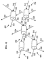
- an embodiment of a multiple level minimum logic interconnect apparatus 100 includes multiple nodes 102 which are connected in a multiple level interconnect structure by interconnect lines 104.
- the multiple level interconnect structure is shown illustratively as a three-dimensional structure to facilitate understanding.
- the nodes 102 in the multiple level interconnect structure are arranged to include multiple levels 110 , each level 110 having a hierarchical significance so that, after a message is initiated in the structure, the messages generally move from an initial level 112 to a final level 114 in the direction of levels of a previous hierarchical significance 116 to levels of a subsequent hierarchical significance 118 .
- each level 110 includes multiple structures which are called rings 120 .
- Each ring 120 includes multiple nodes 102 .
- the term "rings" is used merely to facilitate understanding of the structure of a network in the abstract in which visualization of the structure as a collection of concentric cylindrical levels 110 is useful.
- Figure 1A illustrates message data transmission interconnections between nodes 102 on the various cylindrical levels 110 .
- Figure 1B adds a depiction of message data transmission interconnections between nodes 102 and devices 130 to the interconnections illustrated in Figure 1A .
- Figure 1C further shows message data interconnections between nodes 102 on different levels.
- Figure 1D cumulatively shows the interconnections shown in Figures 1A, 1B and 1C in addition to control interconnections between the nodes 102 .
- the actual physical geometry of an interconnect structure is not to be limited to a cylindrical structure. What is important is that multiple nodes are arranged in a first class of groups and the first class of groups are arranged into a second class of groups. Reference to the first class of groups as rings and the second class of groups as levels is meant to be instructive but not limiting.
- the illustrative interconnect apparatus 100 has a structure which includes a plurality of J+ 1 levels 110 .
- Each level 110 includes a plurality of 2 J K nodes 102 .
- Each level M contains 2 J-M rings 120 , each containing 2 M K nodes 102 .
- the total number of nodes 102 in the entire structure is (J + 1)2 J K.
- the interconnect apparatus 100 also includes a plurality 2 J K devices 130 .
- each device of the 2 J K devices 130 is connected to a data output port of each of the K nodes 102 in each ring of the 2 J rings of the final level 114 .
- a device 130 is a computational unit such as a processor-memory unit or a cluster of processor-memory units and input and output buffers.
- an interconnect structure 200 of a node 102 has three input terminals and three output terminals.
- the input terminals include a first data input terminal 210 , a second data input terminal 212 and a control input terminal 214.
- the output terminals include a first data output terminal 220 , a second data output terminal 222 and a control output terminal 224 .
- the data input and output terminals of a node communicate message data with other nodes.
- the control terminals communicate control bits with other nodes for controlling transmission of message data. The number of control bits for controlling message transmission is efficiently reduced since much of the logic throughout the interconnect structure 200 is determined by timing of the receipt of control bits and message data in a manner to be detailed hereinafter.
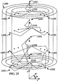
- an interconnect structure 300 is illustrated as a collection of concentric cylinders in three dimensions r, ⁇ and z.
- Each node or device has a location designated (r, ⁇ , z) which relates to a position (r, 2 ⁇ /K, z) in three-dimensional cylindrical coordinates where radius r is an integer which specifies the cylinder number from 0 to J, angle ⁇ is an integer which specifies the spacing of nodes around the circular cross-section of a cylinder from 0 to K-1, and height z is a binary integer which specifies distance along the z-axis from 0 to 2 J -1. Height z is expressed as a binary number because the interconnection between nodes in the z-dimension is most easily described as a manipulation of binary digits. Accordingly, an interconnect structure 300 is defined with respect to two design parameters J and K.
- Figures 3A, 3R and 3C are schematic block diagrams that show interconnections of nodes on various levels of the interconnect structure.
- Figure 3A shows a node A RJ 320 on a ring R of outermost level J and the interconnections of node A RJ 320 to node B RJ 322, device C 324 , node D RJ 326 , node E R(J-1) 328 , node F R(J-1) 330 and device G 332 .
- Figure 3B shows a node A RT 340 on a ring R of a level J and the interconnections of node A RT 340 to node B RT 342 , node C R(T+1) 344 , node D RT 346 , node E R(T-1) 348 , node F R(T-1) 350 and node G R(T+1) 352 .
- Figure 3C shows a node A R0 360 on a ring R of innermost level 0 and the interconnections of node A R0 360 to node B R0 362 , node C R1 364 , node D R0 366 , device E 368 and node G R1 372 .
- ( ⁇ -1)mod K is equal K when ⁇ is equal to 0 and equal to ⁇ -1 otherwise.
- a node 102 on a level T is called a level T node.
- An interconnect structure has J +1 levels and 2 J K nodes on each level.
- the interconnect structure is fully defined by designating the interconnections for each node A 530 of each level T to devices or nodes B 532 , C 534 , D 536 , E 538 , F 540 and G 542 .
- a device e.g. a computational unit of a computer
- a device e.g. a computational unit
- a device e.g. a computational unit
- a device e.g. a computational unit
- Node A(0, ⁇ ,z) 530 is interconnected to receive message data from immediate predecessor node B(0,( ⁇ -1)mod 5,z) 532 on level 0 and to send message data to immediate successor node D(0,( ⁇ +1)mod 5,z) 536 on level 0.
- the interconnection term in the second dimension for nodes B and D is previously defined as H r (z) and h r (Z), respectively, on level zero, H r (z) and h r (Z) are equal to z.
- Node A(0, ⁇ ,z) 530 is also interconnected to receive message data from predecessor node C(1 ,( ⁇ -1)mod 5,z) 534 on level 1 and to send message data to a device E( ⁇ ,z) 53 8.
- Node A(0, ⁇ ,z) 530 is interconnected to receive a control input signal from a device F(( ⁇ -1)mod 5,z) 540 and to send a control output signal to node G(1, ⁇ ,h 1 (z)) 542 on level 1.
- Node A(1, ⁇ ,z) 530 is interconnected to receive message data from immediate predecessor node B(1,( ⁇ -1)mod 5,H 1 (z)) 532 on level 1 and to send message data to immediate successor node D(1( ⁇ +1)mod 5,h 1 (z)) 536 on level 1.
- Height z is expressed as a binary number (base 2) having the form [z 2 ,z 1 ,z 0 ]. For level one, when z is [z 2 ,z 1 ,0] then h 1 (z) and H 1 (z) are both [z 2 ,z 1 ,1].
- Node A(1, ⁇ ,z) 530 is also interconnected to receive message data from predecessor node C(2,( ⁇ -1)mod 5,z) 534 on level 2 and to send message data to successor node E(0,( ⁇ +1)mod 5,z) 538 on level 0.
- Node A(1, ⁇ ,z) 530 is interconnected to receive a control input signal from a node F(0, ⁇ ,H 1 (z)) 540 on level zero and to send a control output signal to node G(2, ⁇ ,h 2 (z)) 542 on level 2.
- Node A(2, ⁇ ,z) 530 is interconnected to receive message data from immediate predecessor node B(2,( ⁇ -1)mod 5,H 2 (z)) 532 on level 2 and to send message data to immediate successor node D(2,( ⁇ +1)mod 5,h 2 (z)) 536 on level 2.
- Height z is expressed as a binary number (base 2) having the form [z 2 ,z 1 ,z 0 ]. For level two, when z is [k 2 ,0,0] then h 2 (z) is [z 2 ,1,0] and H 2 (z) is [z 2 ,1,1].
- Node A(2, ⁇ ,z) 530 is also interconnected to receive message data from predecessor node C(3,( ⁇ -1)mod 5,z) 534 on level 3 and to send message data to successor node E(1 ,( ⁇ + 1)mod 5,z) 538 on level 1.
- Node A(2, ⁇ ,z) 530 is interconnected to receive a control input signal from a node F(1 , ⁇ ,H 2 (z)) 540 on level 1 and to send a control output signal to node G(3, ⁇ ,h 3 (z)) 542 on level 3.
- Node A(3, ⁇ ,z) 530 is interconnected to receive message data from immediate predecessor node B(3 ,( ⁇ -1 )mod 5,H 3 (z)) 532 on level 3 and to send message data to immediate successor node D(3,( ⁇ +1)mod 5,h 3 (z)) 536 on level 3.
- h 3 (z) is [1,0,0]
- H 3 (z) is [1,1,1].
- z is [0,0,1] then h 3 (z) is [1,0,1] and H 3 (z) is [1,1,0].
- h 3 (z) When z is [0,1,0] then h 3 (z) is [1,1,0] and H 3 (z) is [1,0,0]. When z is [0,1,1] then h 3 (z) is [1,1,1] and H 3 (z) is [1,0,1]. When z is [1,0,0] then h 3 (z) is [0,1,0] and H 3 (z) is [0,0,0]. When z is [1,0,1] then h 3 (z) is [0,1,1] and H 3 (z) is [0,0,1]. When z is [1,1,0] then h 3 (z) is [0,0.1] and H 3 (z) is [0,1,0].
- Node A(3, ⁇ ,z) 530 is also interconnected to receive message data from predecessor node C(4,( ⁇ -1)mod 5,z) 534 on level 4 and to send message data to successor node E(2,( ⁇ +1)mod 5,z) 538 on level 2.
- Node A(3, ⁇ ,z) 530 is interconnected to receive a control input signal from a node F(2, ⁇ ,H 3 (z)) 540 on level 2 and to send a control outpu signal to node G(4, ⁇ ,h 4 (z)) 542 on level 4.
- Figure 11 illustrates interconnections between devices 130 and nodes 102 of a ring 120 on the cylindrical level zero 110 .
- a node 102 has three input terminals and three output terminals, including two data input terminals and one control input terminal and two data output terminals and one control output terminal.
- a device 130 has one data input terminal 402 , one control bit input terminal 404 , one data output terminal 406 and one control bit output terminal 408 .
- nodes 102 at the lowest cylindrical level 110 are connected to devices CU( ⁇ ,z).
- the data input terminal 402 of devices CU( ⁇ ,z) are connected to the second data output terminal 222 of nodes N(0, ⁇ ,z).
- the control bit output terminal 408 of devices CU( ⁇ ,z) are connected to the control input terminal 214 of nodes N(0, ⁇ ,z).
- the devices CU( ⁇ ,z) are also connected to nodes N(J, ⁇ ,z) at the outermost cylinder level.
- the data output terminal 406 of devices CU( ⁇ ,z) are connected to the second data input terminal 212 of nodes N(J, ⁇ ,z).
- the control bit input terminal 404 of devices CU( ⁇ ,z) are connected to the control output terminal 224 of nodes N(0, ⁇ ,z).
- Messages are communicated from devices CU(0,z) to nodes N(J,9,z) at the outermost cylindrical level J. Then messages move sequentially inward from the outermost cylindrical level J to level J-1, level J-2 and so forth unit the messages reach level 0 and then enter a device.
- Messages on the outermost cylinder J can reach any of the 2 J rings at level zero.
- messages on any cylindrical level T can reach a node on 2 T rings on level zero.
- Figure 12 illustrates interconnections among nodes 102 of two adjacent cylindrical levels 110 .
- nodes 102 at the T cylindrical level 110 specifically nodes N(T, ⁇ ,z) 450 , have terminals connected to nodes on the T level, the T+1 level and the T-1 level. These connections are such that the nodes N(T, ⁇ ,z) 450 have one data input terminal connected to a node on the same level T and one data input terminal connected to another source, usually a node on the next outer level T+1 but for nodes on the outermost level J, a device is a source.
- nodes N(T, ⁇ ,z) 450 have a first data input terminal 210 which is connected to a first data output terminal 220 of nodes N(T+1, ⁇ -1,z) 425 .
- nodes N(T, ⁇ ,z) 450 have a first data output terminal 220 which is connected to a first data input terminal 210 of nodes N(T-1, ⁇ +1,z) 454.
- the nodes N(T, ⁇ ,z) 450 also have a second data input terminal 212 and a second data output terminal 222 which are connected to nodes 102 on the same level T.
- the second data input terminal 212 of nodes N(T, ⁇ ,z) 450 are connected to the second data output terminal 222 of nodes N(T, ⁇ -1 ,h T (z)) 456 .
- the second data output terminal 222 of nodes N(T, ⁇ ,z) 450 are connected to the second data input terminal 212 of nodes N(T, ⁇ +1,H T (z)) 458 .
- the cylinder height designation H T (z) is determined using an inverse operation of the technique for determining height designation h T -(z).
- the interconnection of nodes from cylindrical height to height (height z to height H T (z) and height h T (z) to height z) on the same level T is precisely defined according to a height transformation technique and depends on the particular level T within which messages are communicated.
- a next height position h T (z) is determined using a process including three steps.
- the first step is repeated, again inverting the binary coefficients below the z J coefficient of the previously inverted, incremented and limited height position.
- the inverse operation for deriving height descriptor H T (z) is determined in the same manner except that, rather than adding the odd number modulus 2 T to the order-inverted bit string, the same odd number modulus 2 T is added to the order-inverted bit string.
- the interconnection between nodes 102 on the same level is notable and highly advantageous for many reasons.
- the interconnection structure resolves contention among messages directed toward the same node.
- the interconnection structure ensures that a message on a particular level that is blocked by messages on the next level makes a complete tour of the messages on that level before any message is in position to block again.
- a message inherently moves to cover all possible paths to the next level.
- a blocking message must cycle through all rings of a level to block a message twice. Consequently, every message is diverted to avoid continuously blocking other messages.
- blocking messages typically proceed to subsequent levels so that overlying messages are not blocked for long.
- a control code is also sent from a control output terminal 224 of the node N(T, ⁇ ,z) 450 to a control input terminal 214 of a node N(t+1, ⁇ ,h T+1 (z)), the node on level T +1 that has a data output terminal connected to a data input terminal of node N(T, ⁇ +1,h T (z)).
- This control code prohibits node N(T+1, ⁇ ,h T+1 (z)) from sending a message to node N(T, ⁇ +1,h T+1 (z)) at the time node N(T, ⁇ ,z) 450 is sending a message to node N(T, ⁇ +1,h T+1 (z)).
- node N(T+1, ⁇ ,h T+1 (z)) is blocked from sending a message to node N(T, ⁇ +1,h T+1 (z)
- the message is deflected to a node on level T +1.
- messages communicated on the same level have priority over messages communicated from another level.
- the second data output terminal 222 of nodes N(T, ⁇ -1 ,H T (z)) are connected to a second data input terminal 212 of nodes N(T, ⁇ ,z) 450 so that nodes N(T, ⁇ ,z) 450 receive messages from nodes N(T, ⁇ -1 ,H T (z)) that are blocked from transmission to nodes N(T-1 , ⁇ H T (z)).
- the control output terminal 224 of nodes N(T-1, ⁇ ,H,-(z)) to the control input terminal 214 of nodes N(T, ⁇ ,z) 450 to warn of a blocked node and to inform nodes N(T, ⁇ ,z) 450 not to send data at this time since no node receives data from two sources at the same time.
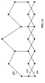
- interconnections of nodes 102 on cylindrical level one exemplify the described interconnections and demonstrate characteristics and advantages that arise from the general interconnection technique.
- the number of nodes K at a cylindrical height is five and the number of heights 2 J is 2 2 , or 4, for a three level (J+1) interconnect structure 500 .
- Nodes N(1, ⁇ ,z) 510 have: (1) a first data input terminal 210 connected to a first data output terminal 220 of nodes N(2, ⁇ -1 ,z) 512 , (2) a control output terminal 224 connected to control input terminal 214 of nodes N(2, ⁇ ,h 2 (z)) 512 , (3) a first data output terminal 220 connected to a first data input terminal 210 of nodes N(0, ⁇ +1 ,z) 516 , (4) a control input terminal 214 connected to a control output terminal 224 of nodes N(0, ⁇ ,H T (z)) 516 , (5) a second data input terminal 212 connected to the second data output terminal 222 of nodes N(1, ⁇ -1 ,H 1 (z)) 520 , and (6) a second data output terminal 222 connected to the second data input terminal 212 of nodes N(1, ⁇ +1,h 1 (z)) 522 .
- height z differs from
- a global clock (not shown) generates timing signals in discrete time steps modulus the number of nodes K at a cylindrical height z of a cylindrical level r.
- messages traverse the interconnect structure 500 on the same level for example, level one
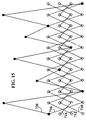
- FIG. 14 interconnections of nodes 102 on cylindrical level two further exemplify described interconnections
- a level two message path 620 is shown overlying the paths 610 and 612 of messages moving on level one.
- the number of nodes K at a cylindrical level is five and the number of levels 2 J is 2 2 , or 4, for a three level (J+ 1) interconnect structur e 500.
- nodes N(2, ⁇ ,z) include: (1) a second data input terminal 212 connected to the second data output terminal 222 of nodes N(2, ⁇ -1,h 2 (z)) and (2) a second data output terminal 222 connected to the second data input terminal 212 of nodes N(2, ⁇ + 1 ,H 2 (z)).
- height z differs from height h 2 (z) and height H 2 (z) only in the final two bit positions.
- bits z and h 2 (z) on cylindrical level two are related as follows: [z J-1 , z J-2 , .
- FIG. 14 illustrates a message blocking condition and its resolution.
- a message m 0 610 is shown at node N 001 and a message m 1 612 at node N 011 .
- a message M 620 on level two at node N 002 is targeted for ring zero.
- message M 620 is blocked and deflected by message m 1 612 to node N 122 at rime one.
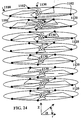
- interconnections of nodes 102 on cylindrical level three show additional examples of previously described interconnections.
- a level three message path 720 is shown overlying the paths 710 , 712 and 714 of messages moving on level two.
- the number of nodes K at a cylindrical height is seven and the number of heights 2 J is 2 3 (8), for a four level (J+1) interconnect structure.
- Same-level interconnections of nodes N(3, ⁇ ,z) include: (1) a second data input terminal 212 connected to the second data output terminal 222 of nodes N(3, ⁇ -1,h 3 (z)) and (2) a second data output terminal 222 connected to the second data input terminal 212 of nodes N(3, ⁇ +1,H 3 (z)).
- Figure 15 illustrates another example of a message blocking condition and its resolution.
- a message m 0 710 is shown at node N 002 , a message m 1 712 at node N 012 , a message m 2 714 at node N 002 and a message m 3 716 at node N 032 .
- a message M 720 on level three at node N 003 is targeted for ring zero. At a time zero, message M 720 is blocked and deflected by message m 3 716 to node N 173 at time one.
- message M 720 moves to node N 233 , message m 0 710 to node N 212 , message m 1 712 to node N 202 , message m 2 714 to node N 232 and message m 3 716 to node N 222 .
- message M 720 is deflected by message m 1 712 .
- message M 720 is blocked by message m 2 714 .
- message M 720 is blocked by message m 0 710 .
- message M , 20 is again blocked by message m 3 716 .
- This alternating blocking of message M 720 by messages m 0 710 , m 1 712 , m 2 714 and m 3 716 continues indefinitely as long as messages m 0 710 , m 1 712 , m 2 714 and m 3 716 are also blocked.
- the described interconnect structure provides that every node N(0, ⁇ ,z) on level zero is accessible by any node N(J, ⁇ ,z) on outermost level J. However, only half of the nodes N(0, ⁇ ,z) on level zero are accessible by a node N(J-1, ⁇ ,z) on the level once removed from the outermost level. Data at a node N(1, ⁇ ,z) on level one can access any node N(0, ⁇ ,z) on level zero so long as the binary representation of height z of level one and the binary representation of ring r of level zero differ only in the last bit.
- data at a node N(2, ⁇ ,z) on level two can access any node N(0, ⁇ ,z) on level zero so long as the binary representation of height z of level two and the binary representation of ring r of level zero differ only in the last two bits.
- a general rule is that, data at a node N(T, ⁇ ,z) on level T can access any node N(0, ⁇ ,z) on level zero so long as the binary representation of height z of level T and the binary representation of ring r of level zero differ only in the last T bits. Accordingly, moving from the outermost level J to level J-1 fixes the most significant bit of the address of the target ring.
- level J-1 to level J-2 fixes the next most significant bit of the address of the target ring and so forth.
- level zero no bits are left to be fixed so that no header bit is tested and a message is always passed to a device.
- an additional header bit is included and tested at a level zero node. This final bit may be used for various purposes, such as for directing message data to a particular buffer of a device when the device accepts the message data.
- An advantage of including an additional bit in the header and performing a bit test at the final node is that all the nodes at all levels of the interconnect structure operate consistently.
- an additional header bit is included in a message packet. This bit indicates that a message packet is being transmitted. Another purpose for such an additional bit in the header is to identify which bit in the header is the control bit.
- a message packet moves from a level T to the next inner level T-1 so long as two conditions are met, as follows: (1) the target ring of the message packet is accessible from level T-1, and (2) the message packet is not blocked by a message on the level T-1.
- any message packet at a node N(T, ⁇ ,z) on a level T that can access its target ring can also access the target ring from a node N(T-1, ⁇ +1,z) only if the bit T-1 of the address ring is the same as bit T-1 of the target ring. Therefore, analysis of only a single bit yields all information for determining a correct routing decision.
- a message packet M at a node N 450 on level four which is targeted for ring two, is potentially blocked by eight message packets m 0 810 , m 1 811 , m 2 812 , m 3 813 , m 4 814 , m 5 815 , m 6 816 and m 7 817 at nodes N 3i0 residing on each of the heights 0 to 7 or level three.
- the behavior of the interconnect structure is analyzed with respect to levels three and four for purposes of illustration, the analysis is applicable to any arbitrary adjacent levels.
- time step zero the message M moves from node N 450 on level four to node N 351 on level three unless a control code is send to node N 450 from a level three node having a data output terminal connected to node M 351 .
- node N 310 has a data output terminal connected to node N 351 and, at time step zero, message m 1 resides at node N 310 . Accordingly, node N 310 sends a control code, in this example a single bit code, to node N 450 , causing deflection of message M to node N 4D1 (where D is a hexadecimal designation of 13) on an interconnection line.
- a bit line illustratively shows the control connection from node N 310 to node N 450 .
- message M moves from node N 4D1 to node N 432 on interconnection line regardless of whether a node N 3D2 is blocked because ring two is not accessible from node N 3D2 .
- message M moves from node N 432 to node N 333 unless a control blocking code is sent from node N 352 to node N 432 where node N 352 is the node on level three that has a data output terminal connected to a data input terminal of node N 333 .
- the message M is blocked from accessing node N 333 because message m 6 currently resides at node N 352 at time step two.
- a deflection control code is sent from node N 352 to node N 432 on control bit line 822 .
- message M is blocked by message m 2 via a control code sent on control bit line.
- message M is blocked by message m 4 though a blocking control code on control bit line.
- the description exemplifies an interconnect structure in which messages descend from an outer level to devices at a core inner layer by advancing one level when the height dimension matches the destination ring location and traversing the rings when the ring location does not match the height designation.
- the messages may move from an inner level to an outer level.
- the heights may be traversed as the level changes and the height held constant as the level remains stationary.
- the progression of messages through nodes is substantially equivalent to the disclosed interconnect structure.
- the advantage of the disclosed network that avoids blocking of messages is negated.
- a timing diagram illustrates timing of message communication in the described interconnect structure.
- control of message communication is determined by timing of message arrival at a node.
- a message packet such as a packet 900 shown in Figure 18, includes a header 910 and a payload 920 .
- the header 910 includes a series of bits 912 designating the target ring in a binary form.
- a source device CU( ⁇ 1 ,z 1 ) at an angle ⁇ 1 and height z 1 sends a message packet M to a destination device CU( ⁇ 2 ,z 2 ) at an angle ⁇ 2 and height z 2
- the bits 912 of header 910 are set to the binary representation of height z 2 .
- a global clock servicing an entire interconnect structure keeps integral time modulus K where, again, K designates the number of nodes n at a cylinder height z.
- K designates the number of nodes n at a cylinder height z.
- ⁇ and ⁇ such that the duration of ⁇ exceeds the duration of ⁇ and the following five conditions are met.
- the amount of time for a message M to exit a node N(T, ⁇ +1 ,h T (z)) on level T after exiting a node N(T, ⁇ ,z) also on level T is ⁇ .
- the amount of time for a message M to exit a node N(T-1, ⁇ +1,z) on level T-1 after exiting a node N(T, ⁇ ,z) on level T is ⁇ - ⁇ .
- the amount of time for a message to travel from a device CU to a node N(r, ⁇ ,z) is ⁇ - ⁇ .
- the message M when a message M moves from a node N(r, ⁇ ,z) to a node N(r, ⁇ +1 ,h r (z)) in time duration ⁇ , the message M also causes a control code to be sent from node N(r, ⁇ ,z) to a node N(r+1, ⁇ +1,h r (z)) to deflect messages on the outer level r + 1.
- the time that elapses from the time that message M enters node N(r, ⁇ ,z) until the control bit arrives at node N(r+ 1, ⁇ + 1,h r+1 (z)) is time duration ⁇ .
- the aforementioned fourth condition also is applicable when a message M moves from a node N(J, ⁇ ,z) to a nude N(J, ⁇ +1,h j (2)) at the outermost level J so that the message is also causes a control code to be sent from node N(J, ⁇ ,z) to a device CU( ⁇ ,z).
- the time that elapses from the time that message M enters node N(r, ⁇ ,z) until the control bit arrives at device CU( ⁇ ,z) is time duration ⁇ .
- the global clock generates timing pulses at a rate of ⁇ .
- the message packet M is sent from a data output terminal of device CU( ⁇ 1 ,z 1 ) to a data input terminal of node N(J, ⁇ 1 ,z 1 ) at the outermost level J.
- Message packets and control bits enter nodes N(T, ⁇ ,z) on a level T at times having the form n ⁇ + L ⁇ where n is a positive integer.
- the message M from device CU( ⁇ 1 ,z 1 ) is sent to the data input terminal of node N(J, ⁇ 1 ,z 1 ) at a time t 0 - ⁇ and is inserted into the data input terminal of node N(J, ⁇ 1 ,z 1 ) at rime t 0 so long as the node N(J, ⁇ 1 ,z 1 ) is not blocked by a control bit resulting from a message traversing on the level J.
- Time t 0 has the form ( ⁇ 2 - ⁇ 1 ) ⁇ +J ⁇ .
- Nodes N(r, ⁇ ,z) include logic that controls routing of messages based on the target address of a message packet M and timing signals from other nodes.
- a first logic switch (not shown) of node N(r, ⁇ ,z) determines whether the message packet M is to proceed to a node N(T-1, ⁇ + 1, z) on the next level T-1 or whether the node N(T-1, ⁇ +1,z) is blocked.
- the first logic switch of node N(r, ⁇ ,z) is set according to whether a single-bit blocking control code sent from node N(T-1, ⁇ ,H T (z)) arrives at node N(r, ⁇ ,z) at a rime t 0 .
- the first logic switch takes a logic 1 value when a node N(T-1, ⁇ +1,z) is blocked and a logic 0 value otherwise.
- a second logic switch (nor shown) of node N(r, ⁇ ,z) determines whether the message packet M is to proceed to a node N(T-1, ⁇ +1 ,z) on the next level T-1 or whether the node N(T-1, ⁇ +1,z) is not in a suitable path for accessing the destination device CU( ⁇ 2 ,z 2 ) of the message packet M.
- the message packet M includes the binary representation of destination height z 2 (z 2(J) , z 2(J-1) , . . , z 2(T) , . .
- the node N(T, ⁇ ,z) on level T includes a single-bit designation z T of the height designation z (z J , z J-1 , . . , z T , . . , z 1 , z 0 ).
- the message packet M proceeds to the next level at node N(T-1, ⁇ +1,z) and the destination height bit z 2(T) is stripped from the header of message packet M.
- the message packet M traverses on the same level T to node N(T, ⁇ +1,h T (z)). If message packet M proceeds to node N(T-1, ⁇ +1,z), then message packet M arrives at a time to + ( ⁇ - ⁇ ) which is equal to a time (z 2 - z 1 + 1) ⁇ + (J - 1) ⁇ . If message packet M traverses to node N(T,0+1,hT(z)), then message packet M arrives at a time L 0 + ⁇ , which is equal to a time (z 2 - z 1 + 1) ⁇ + J ⁇ .
- the message packet M reaches level zero at the designated destination height z 2 . Furthermore, the message packet M reaches the targeted destination device CU( ⁇ 2 ,z 2 ) at a time zero modulus K (the number of nodes at a height z). If the targeted destination device CU( ⁇ 2 ,z 2 ) is ready to accept the message packet M, an input port is activated at time zero modulus K to accept the packet.
- all routing control operations are achieved by comparing two bits. without ever comparing two multiple-bit values. Further advantageously, at the exit point of the interconnect structure as message packers proceed from the nodes to the devices, there is no comparison logic. If a device is prepared to accept a message, the message enters the device via a clock-controlled gate.
- signals that encode bits header typical have a longer duration than bits that encode the payload. Header bits are extended in duration because, as messages communicate through the interconnect structure, timing becomes slightly skewed. Longer duration header bits allow for accurate reading of the bits even when the message is skewed. In contrast, payload bits encode data that is not read during communication trough the interconnect structure.
- the disclosed timing scheme is advantageous because the number of header bits in a message is greatly reduced. Furthermore, in some embodiments the number of header bits is decremented as bits are used for control purposes at each level then discarded while messages pass from level to level in the interconnect structure. In embodiments that discard a control bit for each level of the interconnect structure, logic at each node is simplified since the control bit at each level is located at the same position throughout the interconnect structure.
- That messages communicated on the same level have priority over messages communicated from another level is similarly advantageous because message contention is resolved without carrying priority information in the message header.
- Message contention is otherwise typically resolved by giving priority to messages that have been in an interconnect structure the longest or to predetermined prioritization. These techniques use information stored in the header to resolve contention.
- the interconnect structure and message communication method determines message transmission routing using self-routing decision-making which is local to the nodes and depends on message timing
- both local and global communication control is employed.
- one embodiment of an interconnect structure uses local control which is based on timing to control transmission of message packets in a first transmission mode and alternatively uses global control via a scheduler to administer communication of lengthy strings of message data in a second mode.
- the usage of a scheduler makes the usage of control bit input and output terminals unnecessary.
- the ordering of message packet receipt at a target device may be variable.
- the correct order of message segments is ordered by sending ordering information in the message header.
- Other embodiments employ an optical sorter to order message packets.
- some interconnect node technologies more suitably operate in a routing system utilizing no timing component.
- routing information is contained in additional header bits.
- a designated target device position is included in header bits, for example bits following the designated target ring position.
- the label of a target device is represented as a single logic one in a string of logic zeros.
- the device samples the Nth bit of the device element of the header (as distinguished from the ring element) and accepts the message if the Nth bit is a logic one. This technique is highly suitable for optical node implementations.
- the nodes N(r, ⁇ ,z) have been described in generic terms to refer to various data communication switches for directing data to alternative data paths.
- Node structures which are presently available include electronic nodes, optical nodes and mixed optical/electronic nodes. What is claimed include, for example, interconnect and timing methods, an interconnect apparatus and an interconnect topology. These methods and apparati involve nodes in a generic sense. Thus, the scope of the claims is not limited by the particular type of node described herein and is to extend to any node known now or in the future, which performs the function of the nodes described herein.
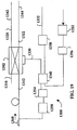
- FIG. 19 One example of a node 1300 is shown, referring to Figure 19 , which includes a lithium niobate (LiNbO3) gate 1302 .
- the lithium niobate gate 1302 has two data input terminals 1310 and 1312 , two data output terminals 1320 and 1322 and one control input terminal 1330.
- Various control circuitry 1340 is added to the lithium niobate gate 1302 to form a control output terminal 1332 of the node 1300.
- Node 1300 also includes optical to electronic converters 1354 , 1356 and 1358 .
- the lithium niobate gate 1302 is forms a 2x2 crossbar. Data paths 1342 and 1344 are optical and the control of the node 1300 is electronic.
- the lithium niobate gate 1302 is combined with a photodetectors 1350 and 1352 and a few electronic logic components to form a node 1300 for various embodiments of an interconnect structure.
- part of the message packet signal 1360 is split off and an appropriate bit of the message packet header (not shown) designating a bit of the binary representation of destination ring in accordance with the discussion hereinbefore, is read by the photodetector 1350 .
- This bit is convened from optical form to an electronic signal.
- This bit a bit designating the cylinder height upon which the node 1300 lies and a bit designating whether a destination node on the next level is blocked are processed electronically and a result of the logical tests of these bits is directed to the control input terminal 1330 of the lithium niobate gate 1302 .
- a logic zero result signal switches the gate in a bar (straight through) state.
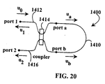
- Node 1400 uses a nonlinear optical loop mirror (NOLM) 1410 to perform a switching function.
- NOLM nonlinear optical loop mirror
- a nonlinear optical loop mirror is a device that makes use of the refractive index of a material to form a completely optical switch that is extremely fast.
- NOLM switch includes a data input terminal 1412 and a control input terminal 1414 . Depending upon the signal at the control input terminal 1414 , data either leaves the NOLM 1410 through the same data input terminal 1412 from which the data entered (hence the term mirror) or the data exits through a data output terminal 1416 . Data is polarized and split into two signal "halves" of equal intensity.
- the two halves of the signal recombine and leave the NOLM 1410 through the data input terminal 1414 .
- the control pulse is polarized at right angles to the data pulse and inserted into the NOLM 1410 so that the control pulse travels with one half of the data pulse.
- the control pulse is more intense than the data pulse and the combined first half of the data pulse and the control pulse quickly pass the second half of the data pulse so that the second half of the data pulse is only minimally accelerated.
- the two halves of the data pulse travel with slightly different velocities and are 180° out of phase when the two halves are recombined. This phase difference causes the combined data pulse signal to pass through the data output terminal 1416 .
- One disadvantage of the NOLM 1410 is that switching is operational only when a long optical transmission loop is employed, thus latency is a problem.
- FIG. 1 another example of a node 1500 is shown which uses a terahertz optical asymmetrical demultiplexer (TOAD) switch 1510 .
- the TOAD switch 1510 is a variation of the NOLM switch 1410 .
- the TOAD 1510 includes an optical fiber loop 1512 and a semiconductor element 1514 , a nonlinear element (NLE) or a semiconductor optical amplifier for example.
- the TOAD switch 1510 has an input data terminal 1520 which also serves as an output data port under some conditions.
- the TOAD switch 1510 also has a separate second output data terminal 1522 .
- the semiconductor element 1514 is placed asymmetrically with respect to the center 1516 of the fiber optic loop 1512 .
- a distance 1518 from the semiconductor element 1514 to the center 1516 of the fiber optic loop 1512 is the distance to transmit one bit of data.
- the TOAD 1510 functions by removing a single bit from a signal having a high data rate.
- the TOAD 1510 is switched by passing a constant electrical current through the semiconductor element 1514 .
- An optical signal entering the semiconductor material causes the index of refraction of the material to immediately change. After the optical signal terminates, the index of refraction slowly (a time span of several bits) drifts back to the level previous to application of the optical signal.
- a control pulse is an optical signal having an intensity higher than that of an optical data signal and polarization at right angles to the optical data signal.
- An optical data input signal is polarized and split into two signal "halves" of equal intensity.
- the control pulse is injected in a manner to move through the fiber optic loop 1512 directly over the bit that is to be removed. Because the distance 1518 is exactly one bit long, one half of the split optical data signal corresponding to a bit leaves the semiconductor element 1514 just as the other half of the bit enters the semiconductor element 1514 . The control pulse only combines with one half of the optical data signal bit so that the velocity of the two halves differs. The combined data and control signal bit exits the TOAD 1510 at the input data terminal 1520 . Thus, this first bit is removed from the data path. A next optical signal bit is split and a first half and second half, moving in opposite directions, are delayed approximately the same amount as the index of refraction of the semiconductor element 1514 gradually changes so that this bit is not removed. After a few bits have passes through the semiconductor element 1514 , the semiconductor material relaxes and another bit is ready to be multiplexed from the optical data signal.
- the TOAD 1510 has a very short optical transmission loop 1512 .
- signal regenerators or amplifiers are used to improve message signal fidelity after messages have passed through a number of nodes.
- a regenerator 1600 is shown which is constructed using a lithium niobate gate 1602 .
- a lithium niobate gate 1602 regenerates message data having a transmission speed of the order of 2.5 gigabits.
- the lithium niobate gate 1602 detects and converts an optical message signal to an electronic signal which drives an electronic input port 1604 of the lithium niobate gate 1602 .
- the lithium niobate gate 1602 is clocked using a clock signal which is applied to one of two optical data ports 1606 and 1608 of the gate 1602 .
- the clock signal is switched by the electronic control pulses and a high fidelity regenerated signal is emitted from the lithium niobate gate 1602 .
- an interconnect structure utilizing a lithium niobate gate 1602 in a regenerator 1600 also uses lithium niobate gates to construct nodes.
- One large power laser (not shown) supplies high fidelity timing pulses to all of the regenerators in an interconnect structure.
- the illustrative regenerator 1600 and node 1650 combination includes an optical coupler 1620 which has a first data input connection to a node on the same level C as the node 1650 and a second data input connection to a node on the overlying level C +1.
- the illustrative regenerator 1600 also includes a photodetector 1622 connected to an output terminal of the optical coupler 1620 , optical to electronic convener 1624 which has an input terminal connected to the optical coupler 1620 through the photodetector 1622 and an output terminal which is connected to the lithium niobate gate 1602 .
- An output terminal of the lithium niobate gate 1602 is connected to a second lithium niobate gate (not shown) of a node (not shown). Two signal lines of the lithium niobate gate (not shown) are combined, regenerated and switched.
- regenerators or amplifiers When regenerators or amplifiers are incorporated to improve signal fidelity and if the time expended by a regenerator or amplifier to recondition a message signal exceeds the time a - ⁇ , then the regenerator or amplifier is placed prior to the input terminal of the node and timing is modified to accommodate the delay.
- interconnect structure shown in Figures 1 through 16 is a simplified structure, meant to easily convey understanding of the principles of the invention. Numerous variations to the basic structure are possible. Various examples of alternative interconnect structures are discussed hereinafter, along with advantages achieved by these alternative structures.
- an alternative embodiment of an interconnect structure 1000 includes devices 1030 which issue message packers to multiple nodes 1002 of the outermost level J.
- a device CU( ⁇ ,z) initiates a message transmission operation by sending a message packet to a node N(J, ⁇ ,z).
- the device CU( ⁇ ,z) initiates a message transmission operation by sending a message packet to node N(J, ⁇ ,z) but, in addition, also includes interconnections to additional multiple nodes N(J, ⁇ ,z) where z designates cylinder heights selected from heights 0 to 2 J of the outermost level J and ⁇ designates node angles selected from angles 0 to K of the heights z.
- the disclosed timing scheme maintains the characteristic that messages arrive at the target node at time zero modulus K.
- Devices are connected to many nodes in the outermost level J to avoid congestion upon entry into the interconnect structure caused by multiple devices sending a series of messages at a high rate to nodes having converging data paths.
- the nodes to which a device is connected are selected at random.
- the multiple interconnection of a device to several nodes is selected in a predetermined manner.
- an alternative embodiment of an interconnect structure 1100 includes devices 1130 which receive message packers from multiple nodes 1102 of the innermost level 0.
- the number of nodes K at a particular height z is nine and each device 1130 is connected to receive message from three nodes on level zero.
- the interconnect structure 1100 is advantageous for improving network exit bandwidth when the number of nodes K on at a particular height is large.
- each node on ring zero is connected to a buffer that has three levels.
- message data is injected into the level zero buffer.
- data is injected into the level one buffer.
- data is injected into the level two buffer.
- a device CU( ⁇ ,0) reads from the level zero buffer at node N(0, ⁇ ,0), from the level one buffer at node N(0,( ⁇ +3)mod 9,0), and from the level two buffer at node N(0,( ⁇ +6)mod 9,0). This reading of message data is accomplished in a synchronous or nonsynchronous manner.
- a time t is expended to transfer data from the buffer to the device.
- the device CU( ⁇ ,0) reads from the level zero buffer at time t , reads from the level three buffer at time 3+ t and reads from the level six buffer at time 6+ t .
- device CU( ⁇ ,0) interconnects to the three buffers as described hereinbefore and reads message data whenever a buffer signals that data is available.
- an alternative embodiment of an interconnect structure 1200 includes devices 1230 which issue message packets to multiple nodes 1202 , not only in the outermost level J but also in other levels.
- the device CU( ⁇ ,z) initiates a message transmission operation by sending a message packet to node N(J, ⁇ ,z) but, in addition, also includes interconnections to additional multiple nodes N(T, ⁇ , z ) where T designates levels of the interconnect structure 1200 , z designates cylinder heights selected from heights 0 to 2 J of the outermost level J and ⁇ designates node angles selected from angles 0 to K of the heights z .
- message communication is controlled according to a priority, as follows. First, messages entering a node N(r, ⁇ ,z) from the same level T have a first priority. Second, messages entering a node N(r, ⁇ ,z) from a higher level T+ 1 have a second priority. Messages entering a node N(r, ⁇ ,z) from a device CU( ⁇ ,z) have last priority.
- the alternative embodiment of interconnect structure 1200 allows a device to send messages to neighboring devices more rapidly.
- the disclosed timing scheme maintains the characteristic that messages arrive at the node designated in the message header at time zero modulus K.
- devices accept data from level zero nodes using one of various predetermined techniques. Some embodiments rely exclusively on timing to determine when the devices accept data so that devices accept data at time zero modulus K. Some embodiments include devices that accept message data at various predetermined times with respect to modulus K timing. Still other embodiments have devices that accept data whenever a buffer is ready to accept data.
- message signal bandwidth is increased using wave division multiplexing.
- a plurality of K colors are defined and generated in a message signal that is transmitted using an interconnect structure having K devices at a cylinder height. Accordingly, each device is assigned a particular color.
- Message packets travel to a preselected target ring in the manner described hereinbefore for a single wavelength interconnect system. Message packets pass from level zero to the appropriate device depending on the color assigned to the message packet.
- a message includes a header and a payload.
- the header and payload are distinguished by having different colors.
- the payload is multiplexed using different colors, which are also different from the color of the header.
- Message bandwidth is also increased by combining different messages of different colors for simultaneous transmission of the messages.
- different messages of different colors are bound on a same target ring, combined an transmitted simultaneously. All messages are not demultiplexed at all of the nodes but, rather, are demultiplexed at input buffers to the devices.
- an interconnect structure has i J cylindrical heights on a level for each of J+ 1 levels, where i is a suitable integer number such as 2 (the previously described embodiment), 3, 4 or more.
- i is a suitable integer number such as 2 (the previously described embodiment), 3, 4 or more.
- each height contains K nodes, and each node has two data input terminals, two data output terminals, one control input terminal and one control output terminal.
- an interconnect structure may have 3 J heights per level. On level one, message data is communicated to one of three level zero heights. On level two, message data is communicated to one of nine level zero heights and so forth.
- This result is achieved as follows. First, the two output data terminals of a node N(r, ⁇ ,z) are connected to input data terminals of a node N(T-1, ⁇ + 1,z) and a node N(T, ⁇ + 1 ,h T (z)), in the manner previously discussed.
- a third height transformation h T (h T (h T (z))) rather than a second height transformation h T (h T (z)) is equal to the original height designation z.
- each level has 3 J heights and a message packet and a message can descend to a lower level every other step.
- variable base i J height structure embodiment whether the target ring is accessible from a particular node is determined by testing a more than one bit of a code designating the target ring.
- the height transformation technique outlined hereinbefore is modified as follows.
- a base three notation height transform technique is utilized rather than the binary height transformation technique discussed previously.
- a target ring is designated by a sequence of base three numbers.
- the base three transformation technique a target ring is designated by a sequence of base three numbers.
- the n low-order base three numbers of the height designation are reversed in order
- the low-order-bit-reversed height designation is incremented by one
- the n low-order base three numbers are reversed back again.
- node N 2(201)3 on level 2 has a first data input terminal connected to a data output terminal of node N 3(201)2 on level 3, a second data input terminal connected to a data output terminal of node N 2(220)2 on level two.
- Node N 2(201)3 also has a first data output terminal connected to a data input terminal of node N 1(201)4 on level one and a second data output terminal connected to a data input terminal of node N 2(211)4 .
- Node N 2(201)3 also has a control input bit connected to a control output bit of node N 1(200)3 and a control output bit connected to a control input bit of node N 3(211)3 .
- the header includes a synch bit followed by the address c a target ring in base three.
- the base three numbers are symbolized in binary form as 00, 01 and 10 or using three bits in the form 001, 010 and 100.
- an interconnect structure of the nodes have ten terminals, including five input terminals and five output terminals.
- the input terminals include three data input terminals and two control input terminals.
- the output terminals include three data output terminals and two control output terminals.
- nodes are generally connected among five adjacent cylindrical levels. Specifically, nodes N(T, ⁇ ,z) at the T cylindrical level have terminals connected to nodes on the T, T+1, T+2, T-1 and T-2 levels. These connections are such that the nodes N(T, ⁇ ,z) have data input terminals connected to nodes on the same level T, the next outer level T+ 1 and the previous outer level T+2.
- nodes N(T, ⁇ ,z) have data input terminals connected to data output terminals of nodes N(T, ⁇ -1,h T (z)), N(T+ 1, ⁇ -1,z) and N(T+2, ⁇ -1,z).
- Nodes N(T, ⁇ ,z) also have control output terminals, which correspond to data input terminals, connected to nodes on the next outer level T+ 1 and the previous outer level T+2.
- Nodes N(T, ⁇ ,z) have control output terminals connected to control input terminals of nodes N(T +1, ⁇ -1,z) and N(T + 2, ⁇ -1,z).
- Nodes N(T, ⁇ ,z) also have data output terminals connected to nodes on the same level T, the next inner level T- 1 and the subsequent inner level T-2.
- nodes N(T, ⁇ ,z) have data output terminals connected to data output terminals of nodes N(T, ⁇ +1,H T (z)), N(T-1, ⁇ +1,z) and N(T-2, ⁇ +1,z).
- Nodes N(T, ⁇ ,z) also have control input terminals, which correspond to data output terminals, connected to nodes on the next inner level T-1 and the subsequent inner level T-2.
- Nodes N(T, ⁇ ,z) have control input terminals connected to control output terminals of nodes N(T-1 , ⁇ + 1,z) and N(T-2, ⁇ + 1 ,z).
- This ten-terminal structure applies only to nodes at the intermediate levels 2 to J-2 since nodes at the outer levels J and 3-1 and at the inner levels 1 and 0 have the same connections as the standard six-terminal nodes.
- This ten-terminal structure allows messages to skip past levels when possible and thereby pass through fewer nodes at the cost of increasing logic at the nodes. Only one message is allowed to enter a node at one time.
- the priority of message access to a node is that a message on the same level has top priority, a message from a node one level removed has second priority and a message from a node two levels away has last priority. Messages descend two levels whenever possible.
- the timing rules for an interconnect structure using the six-terminal nodes are that messages pass more quickly through the levels.
- interconnect structure embodiments include nodes having more than ten terminals so that data and control terminals are connected to additional nodes on additional levels.
- various nodes N(T, ⁇ ,z) also have associated control input terminals and data output terminals, which are connected to nodes on inner levels T-3, T-4 and so on.
- various nodes N(T, ⁇ ,z) also have associated control output terminals and data input terminals, which are connected to nodes on outer levels T+3, T+4 and so on.
- nodes may be connected among all levels or selected levels.
- Additional interconnect structure embodiments utilize additional interconnections among nodes on the same level.
- nodes N(T, ⁇ ,z) on the level T have interconnections in addition to the connections of (1) an output data terminal connected to an input data terminal of nodes N(T, ⁇ +1,h T (z)) and (2) an input data terminal connected to an output data terminal of nodes N(T, ⁇ -1,HT(z)).
- nodes N(T, ⁇ ,z) on the level T have interconnections including a connection of (1) an output data terminal connected to an input data terminal of nodes N(T, ⁇ + 1 ,g T (z)) and (2) an input data terminal connected to an output data terminal of nodes N(T, ⁇ -1,h T (z)).
- height g T (z) is on the half of the interconnect structure of level T that is opposite to the position of height z (meaning bit T of the binary code describing height h T (z) and g T (z) is complementary to bit T of height z).
- a multiple interconnections to a next level embodiment is similar to the multiple interconnections to the same level embodiment except that node N(T, ⁇ ,z) has one output data terminal connected to one node N(T, ⁇ +1,h T (z)) on level T and two output data terminals connected to two nodes N(T-1 , ⁇ +1 ,z) and N(T-1, ⁇ +1,g T-1 (z)) on level T-1.
- one data output interconnection traverses the same level
- a second interconnection progresses one level
- a third interconnection both progresses one level and traverses.
- height g T (z) is on the half of the interconnect structure of level T that is opposite to the position of height z.
- Conflicts between node access are resolved by applying a first priority to messages moving on the same level, a second priority to messages progressing one level and a third priority to messages both progressing one level and traversing.
- interconnect structure which is arranged in multiple dimensions. This reference to dimensions is useful for understanding the interconnect structure topology. However, these dimensions are not limited to spatial dimensions but generally refer to groups of nodes which are interconnected in a particular manner.
Applications Claiming Priority (3)
| Application Number | Priority Date | Filing Date | Title |
|---|---|---|---|
| US08/505,513 US5996020A (en) | 1995-07-21 | 1995-07-21 | Multiple level minimum logic network |
| US505513 | 1995-07-21 | ||
| EP96924569A EP0842473B1 (fr) | 1995-07-21 | 1996-07-19 | Reseau logique minimal aux niveaux multiples |
Related Parent Applications (2)
| Application Number | Title | Priority Date | Filing Date |
|---|---|---|---|
| EP96924569A Division EP0842473B1 (fr) | 1995-07-21 | 1996-07-19 | Reseau logique minimal aux niveaux multiples |
| EP96924569.5 Division | 1997-02-06 |
Publications (2)
| Publication Number | Publication Date |
|---|---|
| EP1058195A2 true EP1058195A2 (fr) | 2000-12-06 |
| EP1058195A3 EP1058195A3 (fr) | 2010-03-10 |
Family
ID=24010615
Family Applications (3)
| Application Number | Title | Priority Date | Filing Date |
|---|---|---|---|
| EP96924569A Expired - Lifetime EP0842473B1 (fr) | 1995-07-21 | 1996-07-19 | Reseau logique minimal aux niveaux multiples |
| EP00120146A Withdrawn EP1058194A3 (fr) | 1995-07-21 | 1996-07-19 | Réseau logique minimal à niveaux multiples |
| EP00120188A Withdrawn EP1058195A3 (fr) | 1995-07-21 | 1996-07-19 | Réseau logique minimal à niveaux multiples |
Family Applications Before (2)
| Application Number | Title | Priority Date | Filing Date |
|---|---|---|---|
| EP96924569A Expired - Lifetime EP0842473B1 (fr) | 1995-07-21 | 1996-07-19 | Reseau logique minimal aux niveaux multiples |
| EP00120146A Withdrawn EP1058194A3 (fr) | 1995-07-21 | 1996-07-19 | Réseau logique minimal à niveaux multiples |
Country Status (14)
| Country | Link |
|---|---|
| US (5) | US5996020A (fr) |
| EP (3) | EP0842473B1 (fr) |
| JP (1) | JP3594198B2 (fr) |
| KR (1) | KR100401682B1 (fr) |
| AT (1) | ATE327537T1 (fr) |
| AU (1) | AU725826B2 (fr) |
| CA (1) | CA2227271C (fr) |
| DE (2) | DE1058195T1 (fr) |
| ES (1) | ES2160556T1 (fr) |
| GR (1) | GR20010300054T1 (fr) |
| HK (1) | HK1010926A1 (fr) |
| MX (1) | MX9800626A (fr) |
| NZ (2) | NZ313016A (fr) |
| WO (1) | WO1997004399A2 (fr) |
Families Citing this family (27)
| Publication number | Priority date | Publication date | Assignee | Title |
|---|---|---|---|---|
| US5996020A (en) | 1995-07-21 | 1999-11-30 | National Security Agency | Multiple level minimum logic network |
| US6289021B1 (en) * | 1997-01-24 | 2001-09-11 | Interactic Holdings, Llc | Scaleable low-latency switch for usage in an interconnect structure |
| US6754207B1 (en) * | 1998-01-20 | 2004-06-22 | Interactic Holdings, Llc | Multiple-path wormhole interconnect |
| US6661816B2 (en) | 1998-06-11 | 2003-12-09 | University Of Central Florida | Multiwavelength modelocked lasers |
| US6801551B1 (en) | 1998-05-15 | 2004-10-05 | University Of Central Florida | Programmable multiwavelength modelocked laser |
| US6314115B1 (en) * | 1998-05-15 | 2001-11-06 | University Of Central Florida | Hybrid WDM-TDM optical communication and data link |
| US6247061B1 (en) * | 1998-06-09 | 2001-06-12 | Microsoft Corporation | Method and computer program product for scheduling network communication packets originating from different flows having unique service requirements |
| US6807667B1 (en) * | 1998-09-21 | 2004-10-19 | Microsoft Corporation | Method and system of an application program interface for abstracting network traffic control components to application programs |
| US6842788B1 (en) * | 2000-10-11 | 2005-01-11 | Nortel Networks Limited | Computing and using resource colors for composite links |
| US7016363B1 (en) * | 2000-10-19 | 2006-03-21 | Interactic Holdings, Llc | Scaleable interconnect structure utilizing quality-of-service handling |
| US7221677B1 (en) * | 2000-10-19 | 2007-05-22 | Interactic Holdings, Llc | Scalable apparatus and method for increasing throughput in multiple level minimum logic networks using a plurality of control lines |
| US20030035371A1 (en) * | 2001-07-31 | 2003-02-20 | Coke Reed | Means and apparatus for a scaleable congestion free switching system with intelligent control |
| CA2544319A1 (fr) * | 2003-10-29 | 2005-05-12 | Interactic Holdings, Llc. | Systemes d'aiguillages paralleles utilisant la correction d'erreurs |
| US20050132089A1 (en) * | 2003-12-12 | 2005-06-16 | Octigabay Systems Corporation | Directly connected low latency network and interface |
| ATE465600T1 (de) * | 2004-03-08 | 2010-05-15 | Interactic Holdings Llc | Hochparallele schaltsysteme mit fehlerkorrektur ii |
| US20060171386A1 (en) * | 2004-09-01 | 2006-08-03 | Interactic Holdings, Llc | Means and apparatus for a scaleable congestion free switching system with intelligent control III |
| EP1836503A4 (fr) * | 2004-12-20 | 2009-09-23 | Interactic Holdings Llc | Interconnexion controlee redimensionnable comprenant des applications optiques et sans fil |
| US8559443B2 (en) | 2005-07-22 | 2013-10-15 | Marvell International Ltd. | Efficient message switching in a switching apparatus |
| US20070076761A1 (en) * | 2005-09-15 | 2007-04-05 | Coke Reed | Apparatus for interconnecting multiple devices to a synchronous device |
| US7895560B2 (en) * | 2006-10-02 | 2011-02-22 | William Stuart Lovell | Continuous flow instant logic binary circuitry actively structured by code-generated pass transistor interconnects |
| EP2092436A4 (fr) | 2006-10-26 | 2010-03-24 | Coke S Reed | Carte réseau pour une utilisation dans des systèmes informatiques en parallèle |
| US7957385B2 (en) * | 2009-03-26 | 2011-06-07 | Terascale Supercomputing Inc. | Method and apparatus for packet routing |
| US7957400B2 (en) * | 2009-03-26 | 2011-06-07 | Terascale Supercomputing Inc. | Hierarchical network topology |
| US20100250784A1 (en) * | 2009-03-26 | 2010-09-30 | Terascale Supercomputing Inc. | Addressing Scheme and Message Routing for a Networked Device |
| US9930117B2 (en) | 2014-09-30 | 2018-03-27 | Interactic Holdings, Llc | Matrix vector multiply techniques |
| WO2016057783A1 (fr) | 2014-10-08 | 2016-04-14 | Interactic Holdings, Llc | Transformée de fourier rapide utilisant un système informatique réparti |
| SG11202106270UA (en) | 2018-12-12 | 2021-07-29 | Interactic Holdings Llc | Method and apparatus for improved data transfer between processor cores |
Citations (1)
| Publication number | Priority date | Publication date | Assignee | Title |
|---|---|---|---|---|
| US5420982A (en) * | 1987-08-19 | 1995-05-30 | Fujitsu Limited | Hyper-cube network control system having different connection patterns corresponding to phase signals for interconnecting inter-node links and between input/output links |
Family Cites Families (26)
| Publication number | Priority date | Publication date | Assignee | Title |
|---|---|---|---|---|
| US4814980A (en) * | 1986-04-01 | 1989-03-21 | California Institute Of Technology | Concurrent hypercube system with improved message passing |
| US4933836A (en) * | 1986-10-29 | 1990-06-12 | United Technologies Corporation | n-Dimensional modular multiprocessor lattice architecture |
| US5339396A (en) * | 1987-11-18 | 1994-08-16 | Hitachi, Ltd. | Interconnection network and crossbar switch for the same |
| US5181017A (en) * | 1989-07-27 | 1993-01-19 | Ibm Corporation | Adaptive routing in a parallel computing system |
| DE69029239T2 (de) * | 1989-09-18 | 1997-03-27 | Fujitsu Ltd | Übertragungsteuerungssystem zwischen Parallelrechnern |
| US5313590A (en) * | 1990-01-05 | 1994-05-17 | Maspar Computer Corporation | System having fixedly priorized and grouped by positions I/O lines for interconnecting router elements in plurality of stages within parrallel computer |
| US5253248A (en) * | 1990-07-03 | 1993-10-12 | At&T Bell Laboratories | Congestion control for connectionless traffic in data networks via alternate routing |
| US5471623A (en) * | 1991-02-26 | 1995-11-28 | Napolitano, Jr.; Leonard M. | Lambda network having 2m-1 nodes in each of m stages with each node coupled to four other nodes for bidirectional routing of data packets between nodes |
| US5224100A (en) * | 1991-05-09 | 1993-06-29 | David Sarnoff Research Center, Inc. | Routing technique for a hierarchical interprocessor-communication network between massively-parallel processors |
| US5524082A (en) * | 1991-06-28 | 1996-06-04 | International Business Machines Corporation | Redundancy removal using quasi-algebraic methods |
| JPH0581216A (ja) * | 1991-09-20 | 1993-04-02 | Hitachi Ltd | 並列プロセツサ |
| US5533198A (en) * | 1992-11-30 | 1996-07-02 | Cray Research, Inc. | Direction order priority routing of packets between nodes in a networked system |
| DE4307174A1 (de) * | 1993-03-08 | 1994-09-15 | Philips Patentverwaltung | Lokales Netzwerk |
| US5617413A (en) * | 1993-08-18 | 1997-04-01 | The United States Of America As Represented By The Administrator Of The National Aeronautics And Space Administration | Scalable wrap-around shuffle exchange network with deflection routing |
| US5546596A (en) * | 1993-08-24 | 1996-08-13 | Intel Corporation | Method and apparatus for integrated local and express routing in a multiprocessor |
| GB9323329D0 (en) * | 1993-11-11 | 1994-01-05 | Philips Electronics Uk Ltd | Communications system |
| US5583990A (en) * | 1993-12-10 | 1996-12-10 | Cray Research, Inc. | System for allocating messages between virtual channels to avoid deadlock and to optimize the amount of message traffic on each type of virtual channel |
| US5485455A (en) * | 1994-01-28 | 1996-01-16 | Cabletron Systems, Inc. | Network having secure fast packet switching and guaranteed quality of service |
| US5544163A (en) * | 1994-03-08 | 1996-08-06 | Excel, Inc. | Expandable telecommunications system |
| EP0691769A1 (fr) * | 1994-07-07 | 1996-01-10 | International Business Machines Corporation | Systèmes d'émulation des circuits de voix dans un réseau de commutation de paquets |
| US5781551A (en) * | 1994-09-15 | 1998-07-14 | Texas Instruments Incorporated | Computer communications system with tree architecture and communications method |
| US5606551A (en) * | 1994-12-21 | 1997-02-25 | Lucent Technologies Inc. | Bidirectional mesh network |
| US5684959A (en) * | 1995-04-19 | 1997-11-04 | Hewlett-Packard Company | Method for determining topology of a network |
| US5577029A (en) * | 1995-05-04 | 1996-11-19 | Interwave Communications | Cellular communication network having intelligent switching nodes |
| US6578010B1 (en) * | 1995-06-05 | 2003-06-10 | George A. Teacherson | Multi-node network marketing computer system |
| US5996020A (en) * | 1995-07-21 | 1999-11-30 | National Security Agency | Multiple level minimum logic network |
-
1995
- 1995-07-21 US US08/505,513 patent/US5996020A/en not_active Expired - Lifetime
-
1996
- 1996-07-19 EP EP96924569A patent/EP0842473B1/fr not_active Expired - Lifetime
- 1996-07-19 ES ES00120188T patent/ES2160556T1/es active Pending
- 1996-07-19 AT AT96924569T patent/ATE327537T1/de not_active IP Right Cessation
- 1996-07-19 DE DE1058195T patent/DE1058195T1/de active Pending
- 1996-07-19 NZ NZ313016A patent/NZ313016A/xx not_active IP Right Cessation
- 1996-07-19 WO PCT/US1996/011828 patent/WO1997004399A2/fr active IP Right Grant
- 1996-07-19 NZ NZ503094A patent/NZ503094A/en not_active IP Right Cessation
- 1996-07-19 EP EP00120146A patent/EP1058194A3/fr not_active Withdrawn
- 1996-07-19 CA CA002227271A patent/CA2227271C/fr not_active Expired - Fee Related
- 1996-07-19 EP EP00120188A patent/EP1058195A3/fr not_active Withdrawn
- 1996-07-19 AU AU64988/96A patent/AU725826B2/en not_active Ceased
- 1996-07-19 JP JP50682297A patent/JP3594198B2/ja not_active Expired - Fee Related
- 1996-07-19 KR KR10-1998-0700415A patent/KR100401682B1/ko not_active IP Right Cessation
- 1996-07-19 DE DE69636165T patent/DE69636165D1/de not_active Expired - Fee Related
-
1998
- 1998-01-21 MX MX9800626A patent/MX9800626A/es not_active IP Right Cessation
- 1998-11-20 HK HK98112191A patent/HK1010926A1/xx not_active IP Right Cessation
-
1999
- 1999-09-14 US US09/397,333 patent/US6272141B1/en not_active Expired - Lifetime
-
2001
- 2001-05-07 US US09/852,009 patent/US7068671B2/en not_active Expired - Fee Related
- 2001-05-07 US US09/850,953 patent/US20010034798A1/en not_active Abandoned
- 2001-10-31 GR GR20010300054T patent/GR20010300054T1/el unknown
-
2004
- 2004-06-16 US US10/773,693 patent/US7426214B2/en not_active Expired - Fee Related
Patent Citations (1)
| Publication number | Priority date | Publication date | Assignee | Title |
|---|---|---|---|---|
| US5420982A (en) * | 1987-08-19 | 1995-05-30 | Fujitsu Limited | Hyper-cube network control system having different connection patterns corresponding to phase signals for interconnecting inter-node links and between input/output links |
Non-Patent Citations (5)
| Title |
|---|
| GAUGHAN P T ET AL: "ADAPTIVE ROUTING PROTOCOLS FOR HYPERCUBE INTERCONNECTION NETWORKS" COMPUTER, vol. 26, no. 5, 1 May 1993 (1993-05-01), page 12, XP000365279 * |
| KWONG W C ET AL: "ULTRAFAST ALL-OPTICAL PHOTONIC PACKET SWITCHING" PROCEEDINGS OF THE SPIE - THE INTERNATIONAL SOCIETY FOR OPTICAL ENGINEERING, SPIE, US, vol. 2024, 13 July 1993 (1993-07-13), pages 150-170, XP009003294 ISSN: 0277-786X * |
| MALEK M ET AL: "THE CYLINDRICAL BANYAN MULTICOMPUTER: A RECONFIGURABLE SYSTOLIC ARCHITECTURE" PARALLEL COMPUTING, vol. 10, no. 3, 1 May 1989 (1989-05-01), pages 319-327, XP000065558 * |
| RAVIKUMAR C P ET AL: "Star-Graph based multistage interconnection network for ATM switch fabric" PARALLEL AND DISTRIBUTED PROCESSING, 1994. PROCEEDINGS. SIXTH IEEE SYM POSIUM ON DALLAS, TX, USA 26-29 OCT. 1994, LOS ALAMITOS, CA, USA,IEEE COMPUT. SOC, 26 October 1994 (1994-10-26), pages 444-451, XP010100155 ISBN: 978-0-8186-6427-4 * |
| YOUNG S D ET AL: "Adaptive routing in generalized hypercube architectures" PROCEEDINGS OF THE THIRD IEEE SYMPOSIUM ON PARALLEL AND DISTRIBUTED PROCESSING (CAT. NO.91TH0396-2), DALLAS, TX, USA, 2-5 DEC. 1991, 1 January 1991 (1991-01-01), pages 564-571, XP002024983 ISBN 0-8186-2310-1, 1991, LOS ALAMITOS, CA, USA, IEEE COMPUT. SOC. PRESS, USA * |
Also Published As
| Publication number | Publication date |
|---|---|
| EP0842473B1 (fr) | 2006-05-24 |
| KR19990035759A (ko) | 1999-05-25 |
| WO1997004399A2 (fr) | 1997-02-06 |
| DE1058195T1 (de) | 2001-10-25 |
| CA2227271A1 (fr) | 1997-02-06 |
| AU6498896A (en) | 1997-02-18 |
| US5996020A (en) | 1999-11-30 |
| JP3594198B2 (ja) | 2004-11-24 |
| CA2227271C (fr) | 2002-12-31 |
| GR20010300054T1 (en) | 2001-10-31 |
| US6272141B1 (en) | 2001-08-07 |
| US7068671B2 (en) | 2006-06-27 |
| EP0842473A2 (fr) | 1998-05-20 |
| ATE327537T1 (de) | 2006-06-15 |
| EP1058194A3 (fr) | 2010-03-10 |
| HK1010926A1 (en) | 1999-07-02 |
| US20070186008A1 (en) | 2007-08-09 |
| MX9800626A (es) | 1998-11-30 |
| EP1058195A3 (fr) | 2010-03-10 |
| WO1997004399A3 (fr) | 1997-04-10 |
| NZ503094A (en) | 2001-11-30 |
| US20010021192A1 (en) | 2001-09-13 |
| JP2000500253A (ja) | 2000-01-11 |
| US7426214B2 (en) | 2008-09-16 |
| EP1058194A2 (fr) | 2000-12-06 |
| AU725826B2 (en) | 2000-10-19 |
| DE69636165D1 (de) | 2006-06-29 |
| US20010034798A1 (en) | 2001-10-25 |
| ES2160556T1 (es) | 2001-11-16 |
| KR100401682B1 (ko) | 2004-02-05 |
| NZ313016A (en) | 2000-05-26 |
Similar Documents
| Publication | Publication Date | Title |
|---|---|---|
| US7068671B2 (en) | Multiple level minimum logic network | |
| US6289021B1 (en) | Scaleable low-latency switch for usage in an interconnect structure | |
| KR100324092B1 (ko) | 통신네크워크및이통신네트워크의이용방법 | |
| JP2595025B2 (ja) | 空間分割形スイッチを用いた高速パケット交換装置 | |
| US7397808B2 (en) | Parallel switching architecture for multiple input/output | |
| US9825844B2 (en) | Network topology of hierarchical ring with recursive shortcuts | |
| US5617413A (en) | Scalable wrap-around shuffle exchange network with deflection routing | |
| CA2302260C (fr) | Reseau de communication | |
| WO2000076256A1 (fr) | Commutateur photonique utilisant l'echange de creneaux | |
| WO2002093843A1 (fr) | Systeme de routage | |
| Callegati et al. | Design of a WDM optical packet switch for IP traffic | |
| AU768042B2 (en) | Multiple level minimum logic network | |
| AU2004200799A1 (en) | Multiple level minimum logic network | |
| Cotter et al. | Ultrafast all-optical signal processing for packet switching | |
| Liu et al. | Time division multiplexed de Bruijn network and ShuffleNet for optical communications | |
| Wang et al. | Contention resolution in the loop-augmented shufflenet multihop lightwave network | |
| JPH0427243A (ja) | Atmセル集線方式 | |
| GB2357656A (en) | Optical packet router | |
| JPH02288439A (ja) | セルスイッチ | |
| JP2000069048A (ja) | Atmスイッチ | |
| JPH02186792A (ja) | 多入力1出力光バッファ |
Legal Events
| Date | Code | Title | Description |
|---|---|---|---|
| PUAI | Public reference made under article 153(3) epc to a published international application that has entered the european phase |
Free format text: ORIGINAL CODE: 0009012 |
|
| AC | Divisional application: reference to earlier application |
Ref document number: 842473 Country of ref document: EP |
|
| AK | Designated contracting states |
Kind code of ref document: A2 Designated state(s): AT BE CH DE DK ES FI FR GB GR IE IT LI NL PT SE |
|
| EL | Fr: translation of claims filed | ||
| TCAT | At: translation of patent claims filed | ||
| DET | De: translation of patent claims | ||
| REG | Reference to a national code |
Ref country code: ES Ref legal event code: BA2A Ref document number: 2160556 Country of ref document: ES Kind code of ref document: T1 |
|
| TCNL | Nl: translation of patent claims filed | ||
| PUAL | Search report despatched |
Free format text: ORIGINAL CODE: 0009013 |
|
| REG | Reference to a national code |
Ref country code: HK Ref legal event code: WD Ref document number: 1034124 Country of ref document: HK |
|
| AK | Designated contracting states |
Kind code of ref document: A3 Designated state(s): AT BE CH DE DK ES FI FR GB GR IE IT LI NL PT SE |
|
| RIC1 | Information provided on ipc code assigned before grant |
Ipc: H04L 12/56 20060101ALI20100201BHEP Ipc: G06F 15/173 20060101AFI20100201BHEP |
|
| 17P | Request for examination filed |
Effective date: 20100910 |
|
| AKX | Designation fees paid |
Designated state(s): AT BE CH DE DK ES FI FR GB GR IE IT LI NL PT SE |
|
| STAA | Information on the status of an ep patent application or granted ep patent |
Free format text: STATUS: THE APPLICATION IS DEEMED TO BE WITHDRAWN |
|
| 18D | Application deemed to be withdrawn |
Effective date: 20130103 |