EP1058162B1 - Wechselstromskorotron - Google Patents
Wechselstromskorotron Download PDFInfo
- Publication number
- EP1058162B1 EP1058162B1 EP00109989A EP00109989A EP1058162B1 EP 1058162 B1 EP1058162 B1 EP 1058162B1 EP 00109989 A EP00109989 A EP 00109989A EP 00109989 A EP00109989 A EP 00109989A EP 1058162 B1 EP1058162 B1 EP 1058162B1
- Authority
- EP
- European Patent Office
- Prior art keywords
- grid
- wires
- image area
- image
- wire
- Prior art date
- Legal status (The legal status is an assumption and is not a legal conclusion. Google has not performed a legal analysis and makes no representation as to the accuracy of the status listed.)
- Expired - Lifetime
Links
- 150000002500 ions Chemical class 0.000 claims description 7
- 238000003384 imaging method Methods 0.000 claims description 4
- 238000000034 method Methods 0.000 description 18
- 238000011161 development Methods 0.000 description 17
- 108091008695 photoreceptors Proteins 0.000 description 17
- 230000008569 process Effects 0.000 description 17
- 239000000843 powder Substances 0.000 description 11
- 238000007639 printing Methods 0.000 description 10
- 238000012546 transfer Methods 0.000 description 10
- 230000001965 increasing effect Effects 0.000 description 8
- 239000000758 substrate Substances 0.000 description 5
- 239000000463 material Substances 0.000 description 4
- 230000003247 decreasing effect Effects 0.000 description 3
- 238000005259 measurement Methods 0.000 description 3
- 238000012545 processing Methods 0.000 description 3
- 238000000926 separation method Methods 0.000 description 3
- 230000001629 suppression Effects 0.000 description 3
- 230000005540 biological transmission Effects 0.000 description 2
- 238000004140 cleaning Methods 0.000 description 2
- 230000001276 controlling effect Effects 0.000 description 2
- 238000000151 deposition Methods 0.000 description 2
- 230000000694 effects Effects 0.000 description 2
- 239000002245 particle Substances 0.000 description 2
- 230000001850 reproductive effect Effects 0.000 description 2
- 239000000523 sample Substances 0.000 description 2
- 230000001154 acute effect Effects 0.000 description 1
- 230000003466 anti-cipated effect Effects 0.000 description 1
- 238000013459 approach Methods 0.000 description 1
- 230000009286 beneficial effect Effects 0.000 description 1
- 230000015572 biosynthetic process Effects 0.000 description 1
- 239000002131 composite material Substances 0.000 description 1
- 230000001010 compromised effect Effects 0.000 description 1
- 238000011109 contamination Methods 0.000 description 1
- 230000001419 dependent effect Effects 0.000 description 1
- 230000008021 deposition Effects 0.000 description 1
- 230000002708 enhancing effect Effects 0.000 description 1
- 230000006872 improvement Effects 0.000 description 1
- 239000012212 insulator Substances 0.000 description 1
- 230000003993 interaction Effects 0.000 description 1
- 238000007648 laser printing Methods 0.000 description 1
- 239000011159 matrix material Substances 0.000 description 1
- 230000001105 regulatory effect Effects 0.000 description 1
- 230000004044 response Effects 0.000 description 1
- 239000007921 spray Substances 0.000 description 1
- 230000003068 static effect Effects 0.000 description 1
Images


Classifications
-
- G—PHYSICS
- G03—PHOTOGRAPHY; CINEMATOGRAPHY; ANALOGOUS TECHNIQUES USING WAVES OTHER THAN OPTICAL WAVES; ELECTROGRAPHY; HOLOGRAPHY
- G03G—ELECTROGRAPHY; ELECTROPHOTOGRAPHY; MAGNETOGRAPHY
- G03G15/00—Apparatus for electrographic processes using a charge pattern
- G03G15/02—Apparatus for electrographic processes using a charge pattern for laying down a uniform charge, e.g. for sensitising; Corona discharge devices
- G03G15/0291—Apparatus for electrographic processes using a charge pattern for laying down a uniform charge, e.g. for sensitising; Corona discharge devices corona discharge devices, e.g. wires, pointed electrodes, means for cleaning the corona discharge device
Definitions
- the present invention relates generally to a corona device primarily for use in reproduction systems of the xerographic or dry copying type, more particularly, concerning the utilization of field enhancement electrode to extend the charging capabilities of scorotrons.
- the process of electrostatographic copying is initiated by exposing a light image of an original document onto a substantially uniformly charged photoreceptive member. Exposing the charged photoreceptive member to a light image discharges a photoconductive surface thereon in areas corresponding to non-image areas in the original document while maintaining the charge in image areas, thereby creating an electrostatic latent image of the original document on the photoreceptive member. This latent image is subsequently developed into a visible image by depositing charged developing material onto the photoreceptive member such that the developing material is attracted to the charged image areas on the photoconductive surface.
- the developing material is transferred from the photoreceptive member to a copy sheet or to some other image support substrate to create an image which may be permanently affixed to the image support substrate, thereby providing an electrophotographic reproduction of the original document.
- the photoconductive surface of the photoreceptive member is cleaned to remove any residual developing material which may be remaining on the surface thereof in preparation for successive imaging cycles.
- electrostatographic copying process described hereinabove is well known and is commonly used for light lens copying of an original document.
- Analogous processes also exist in other electrostatographic printing applications such as, for example, digital laser printing where a latent image is formed on the photoconductive surface via a modulated laser beam, or ionographic printing and reproduction where charge is deposited on a charge retentive surface in response to electronically generated or stored images.
- image on image processing superimposes toner powder images of different color toners onto the photoreceptor prior to the transfer of the composite toner powder image onto the substrate.
- image on image process has several benefits, it has several problems. For example, when recharging the photoreceptor in preparation for creating another color toner powder image it is important to level the voltages uniformly between the previously toned and the untoned areas of the photoreceptor in a manner that minimizes toner charge throughout the layer without reversing it's polarity.
- a screen controlled device called a scorotron which consists of one or more fine wires supported on insulated blocks spaced between the photoconductive surface and a conductive or insulative surface parallel to it.
- the conductive surface may be grounded or biased.
- a screen or grid is interposed between the corona wires and the photoconductive plate and the grid is maintained at a potential roughly equal to the potential desired on the plate.
- ions from the corona wires will pass between the grid wires and continue on to the plate as long as the potential difference between the grid and the plate exceeds a minimum value. Ideally, when the plate has reached sufficient charge that it is potentially matched to that of the grid, charging will cease. While these devices provide good control and excellent reproducibility of potential, they require power sources for both corona wires and the screen and, are typically bulky occupying considerable space in the machine.
- a charging device according to the invention is defined in claim 7.
- the charging device further comprises second wire electrodes spaced from said first mentioned wires and substantially equally spaced from said second wire electrodes.
- FIG. 1 there is shown an illustrative electrophotographic machine having incorporated therein the development apparatus of the present invention.
- An electrophotographic printing machine 8 creates a color image in a single pass through the machine and incorporates the features of the present invention.
- the printing machine 8 uses a charge retentive surface in the form of an Active Matrix (AMAT) photoreceptor belt 10 which travels sequentially through various process stations in the direction indicated by the arrow 12. Belt travel is brought about by mounting the belt about a drive roller 14 and two tension rollers 16 and 18 and then rotating the drive roller 14 via a drive motor 20.
- AMAT Active Matrix
- the image area is that part of the photoreceptor belt which is to receive the toner powder images which, after being transferred to a substrate, produce the final image. While the photoreceptor belt may have numerous image areas, since each image area is processed in the same way, a description of the typical processing of one image area suffices to fully explain the operation of the printing machine.
- FIG. 1 illustrates a typical voltage profile 68 of an image area after that image area has left the charging station A. As shown, the image area has a uniform potential of about -500 volts. In practice, this is accomplished by charging the image area slightly more negative than -500 volts so that any resulting dark decay reduces the voltage to the desired -500 volts. While Figure 2 shows the image area as being negatively charged, it could be positively charged if the charge levels and polarities of the toners, recharging devices, photoreceptor, and other relevant regions or devices are appropriately changed.
- the now charged image area passes through a first exposure station B.
- the charged image area is exposed to light which illuminates the image area with a light representation of a first color (say black) image. That light representation discharges some parts of the image area so as to create an electrostatic latent image.
- a laser based output scanning device 24 as a light source, it is to be understood that other light sources, for example an LED printbar, can also be used with the principles of the present invention.
- Figure 3 shows typical voltage levels, the levels 72 and 74, which might exist on the image area after exposure.
- the now exposed image area passes through a first development station C which is identical in structure with development system E, G, and I.
- the first development station C deposits a first color, say black, of negatively charged toner 31 onto the image area. That toner is attracted to the less negative sections of the image area and repelled by the more negative sections. The result is a first toner. powder image on the image area.
- the development system includes a donor roll which develops the image on the photoconductive surface.
- the recharging station D is comprised of a corona recharging device, a recharging device 36 of the present invention, which acts to recharge the voltage levels of both the toned and untoned parts of the image area to a substantially uniform level.
- Figure 5 shows the voltages on the image area after it passes through the recharging device 36.
- the recharging device charges the image area.
- the now substantially uniformly charged image area with its first toner powder image passes to a second exposure station 38.
- the second exposure station 38 is the same as the first exposure station B.
- Figure 6 illustrates the potentials on the image area after it passes through the second exposure station. As shown, the non-illuminated areas have a potential about -500 as denoted by the level 84. However, illuminated areas, both the previously toned areas denoted by the toner 76 and the untoned areas are discharged to about -50 volts as denoted by the level 88.
- the image area then passes to a second development station E. Except for the fact that the second development station E contains a toner 40 which is of a different color (yellow) than the toner 31 (black) in the first development station C, the second development station is substantially the same as the first development station. Since the toner 40 is attracted to the less negative parts of the image area and repelled by the more negative parts, after passing through the second development station E the image area has first and second toner powder images which may overlap.
- the now recharged image area then passes through a third recharging station H.
- the third recharging station includes recharge device 61 which adjusts the voltage level of both the toned and untoned parts of the image area to a substantially uniform level in a manner similar to the recharging device 36 and recharging device 51.
- the now recharged image area After passing through the third recharging station the now recharged image area then passes through a fourth exposure station 63. Except for the fact that the fourth exposure station illuminates the image area with a light representation of a fourth color image (say cyan) so as to create a fourth electrostatic latent image, the fourth exposure station 63 is the same as the first, second, and third exposure stations, the exposure stations B, 38, and 53, respectively.
- the fourth electrostatic latent image is then developed using a fourth color toner 65 (cyan) contained in a fourth development station I.
- the image area then passes to a pretransfer corotron member 50 which delivers corona charge to ensure that the toner particles are of the required charge level and polarity so as to ensure proper subsequent transfer.
- the four toner powder images are transferred from the image area onto a support sheet 57 at transfer station J.
- the transfer station J includes a transfer corona device 54 which sprays positive ions onto the backside of sheet 57. This causes the negatively charged toner powder images to move onto the support sheet 57.
- the transfer station J also includes a detack corona device 56 which facilitates the removal of the support sheet 52 from the printing machine 8.
- the various machine functions described above are generally managed and regulated by a controller which provides electrical command signals for controlling the operations described above.
- a scorotron 22 which consists of one or more fine wires 202 supported on insulated blocks 204 spaced between the photoconductive surface and a conductive or insulative surface 206 parallel to it.
- a screen 208 or grid is interposed between the corona wires 202 and the photoconductive surface and the grid is maintained at a potential roughly equal to the potential desired on the photoconductive .
- the scorotrons geometry, the individual wires are from 1/2 to 11/2 inches apart and are spaced from the grid by about 3/4 of an inch.
- Enhancement electrodes 210 are placed on screen 208 and are biased at the same potential as the screen 208.
- the ReaD IOI color process requires a level of voltage nonuniformity that cannot exceed a few volts.
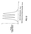
- These characteristics are a static measurement of the magnitude of current delivered to a conductive equipotential plane placed beneath the device as a function of the potential difference between the scorotron DC grid bias and that which is applied to the conductive plane (plate voltage). Theoretically, the current to the conductive plane passes through zero when the grid-plate potential difference is zero. This point is referred to as the voltage intercept (V intercept ) and corresponds to the plate voltage where the current null occurs for a given grid bias.
- V final V intercept ( 1-e -S/Cv ) + V in e -S/Cv
- V final final charge potential on the dielectric
- V in initial dielectric surface potential presented to the charge device.
- V intercept ⁇ V grid conductive plate voltage at which the current passes through zero for a given grid voltage.
- C dielectric capacitance per unit area
- V process velocity
- S slope of the I-V characteristics
Landscapes
- Physics & Mathematics (AREA)
- Engineering & Computer Science (AREA)
- Plasma & Fusion (AREA)
- General Physics & Mathematics (AREA)
- Electrostatic Charge, Transfer And Separation In Electrography (AREA)
Claims (10)
- Eine elektrostatografische, bilderzeugende Vorrichtung, welche mindestens eine Ladeeinrichtung einsetzt zum Laden einer Oberfläche, wobei die mindestens eine Ladeeinrichtung umfasst:ein koronaerzeugendes Element (202) zur Erzeugung von geladenen Ionen; undein Gitter (208), welches auf ein Gitterpotenzial vorgespannt ist und welches von dem koronaerzeugenden Element beabstandet ist, wobei das Gitter ermöglicht, dass Ionen zwischen den Gitterdrähten durchtreten und sich auf die Oberfläche weiterbewegen, bis die Oberfläche eine ausreichende Ladung erhalten hat, welche das Gitterpotenzial annähert; undeine Elektrode (210), welche auf dem Gitter angeordnet ist und welche mit dem Gitter (208) zusammenwirkt, um die Gleichförmigkeit der Ladung auf der Oberfläche zu verbessern.
- Die Vorrichtung gemäß Anspruch 1, wobei das koronaerzeugende Element (202) ein Draht ist.
- Die Vorrichtung gemäß Anspruch 1, wobei die Elektrode auf das Gitterpotenzial vorgespannt ist.
- Die Vorrichtung gemäß Anspruch 1, wobei die Elektrode ein runder Stab ist, welcher einen Durchmesser zwischen 1 mm und 4 mm aufweist.
- Die Vorrichtung gemäß Anspruch 2, wobei das koronaerzeugende Element mindestens drei beabstandete Drähte (202) umfasst, wobei die Vorrichtung weiterhin zweite Elektroden (210) umfasst, wobei die Drähte und die zweiten Elektroden (210) auf dem halben Weg zwischen jeweiligen Paaren von Drähten (202) angeordnet sind.
- Die Vorrichtung gemäß Anspruch 5, wobei die mindestens drei beabstandeten Drähte gleich beabstandet sind.
- Eine Ladungseinrichtung zum Aufladen einer Oberfläche, umfassend:ein koronaerzeugendes Element (202) zur Erzeugung von geladenen Ionen; undein Gitter (208), welches auf ein Gitterpotenzial vorgespannt ist und welches von dem koronaerzeugenden Element beabstandet ist, wobei das Gitter ermöglicht, dass Ionen zwischen den Gitterdrähten durchtreten und sich auf die Oberfläche weiterbewegen, bis die Oberfläche eine ausreichende Ladung erhalten hat, welche das Gitterpotenzial annähert; undeine Elektrode (210), welche auf dem Gitter angeordnet ist und welche mit dem Gitter (208) zusammenwirkt, um die Gleichförmigkeit der Ladung auf der Oberfläche zu verbessern.
- Die Ladungseinrichtung gemäß Anspruch 7, wobei das koronaerzeugende Element (202) ein Draht ist.
- Die Ladungseinrichtung gemäß Anspruch 7, wobei die Elektrode (210) auf das Gitterpotenzial vorgespannt ist.
- Die Ladungseinrichtung gemäß Anspruch 7, wobei die Elektrode (210) ein runder Stab ist, welcher einen Durchmesser zwischen 1 mm und 4 mm aufweist.
Applications Claiming Priority (2)
| Application Number | Priority Date | Filing Date | Title |
|---|---|---|---|
| US311870 | 1999-05-14 | ||
| US09/311,870 US6097915A (en) | 1999-05-14 | 1999-05-14 | AC scorotron |
Publications (3)
| Publication Number | Publication Date |
|---|---|
| EP1058162A2 EP1058162A2 (de) | 2000-12-06 |
| EP1058162A3 EP1058162A3 (de) | 2001-08-29 |
| EP1058162B1 true EP1058162B1 (de) | 2004-11-17 |
Family
ID=23208868
Family Applications (1)
| Application Number | Title | Priority Date | Filing Date |
|---|---|---|---|
| EP00109989A Expired - Lifetime EP1058162B1 (de) | 1999-05-14 | 2000-05-11 | Wechselstromskorotron |
Country Status (5)
| Country | Link |
|---|---|
| US (1) | US6097915A (de) |
| EP (1) | EP1058162B1 (de) |
| JP (1) | JP2000347480A (de) |
| BR (1) | BR0001752B1 (de) |
| DE (1) | DE60015852T2 (de) |
Families Citing this family (3)
| Publication number | Priority date | Publication date | Assignee | Title |
|---|---|---|---|---|
| US6459873B1 (en) * | 2000-11-15 | 2002-10-01 | Xerox Corporation | DC pin scorotron charging apparatus, and printing machine arranged with the same |
| US20060269325A1 (en) * | 2005-05-31 | 2006-11-30 | Xerox Corporation | Charging device for xerographic printing apparatus having enhanced voltage uniformity and enhanced handling robustness |
| JP2015165275A (ja) * | 2014-03-03 | 2015-09-17 | コニカミノルタ株式会社 | 湿式現像装置および湿式画像形成装置 |
Family Cites Families (4)
| Publication number | Priority date | Publication date | Assignee | Title |
|---|---|---|---|---|
| JPS54156546A (en) * | 1978-05-31 | 1979-12-10 | Olympus Optical Co Ltd | Corona charger |
| JPH0616196B2 (ja) * | 1984-03-27 | 1994-03-02 | 日本電信電話株式会社 | 記録装置 |
| US5613172A (en) * | 1995-08-25 | 1997-03-18 | Xerox Corporation | Hybrid DC recharge method and apparatus for split recharge imaging |
| US5655186A (en) * | 1996-03-28 | 1997-08-05 | Xerox Corporation | Light blocking ion charging apparatus |
-
1999
- 1999-05-14 US US09/311,870 patent/US6097915A/en not_active Expired - Lifetime
-
2000
- 2000-05-02 JP JP2000133142A patent/JP2000347480A/ja active Pending
- 2000-05-11 DE DE60015852T patent/DE60015852T2/de not_active Expired - Lifetime
- 2000-05-11 EP EP00109989A patent/EP1058162B1/de not_active Expired - Lifetime
- 2000-05-12 BR BRPI0001752-3A patent/BR0001752B1/pt not_active IP Right Cessation
Also Published As
| Publication number | Publication date |
|---|---|
| JP2000347480A (ja) | 2000-12-15 |
| US6097915A (en) | 2000-08-01 |
| DE60015852D1 (de) | 2004-12-23 |
| BR0001752B1 (pt) | 2012-10-30 |
| BR0001752A (pt) | 2001-01-02 |
| DE60015852T2 (de) | 2005-03-31 |
| EP1058162A2 (de) | 2000-12-06 |
| EP1058162A3 (de) | 2001-08-29 |
Similar Documents
| Publication | Publication Date | Title |
|---|---|---|
| US5010367A (en) | Dual AC development system for controlling the spacing of a toner cloud | |
| US5890030A (en) | Electrostatic image forming apparatus | |
| US6173148B1 (en) | Image forming apparatus with a transfer member having an inherent volume resistance less than that of an inner layer of a transport support element | |
| US5144371A (en) | Dual AC/dual frequency scavengeless development | |
| JPH08220823A (ja) | 印刷機 | |
| EP0715224B1 (de) | Verfahren und Vorrichtung zur Erzeugung von mehreren Bildern | |
| US4205322A (en) | Electrostatic method of simultaneously transferring to a recording medium a toner image having different polarities | |
| US5038177A (en) | Selective pre-transfer corona transfer with light treatment for tri-level xerography | |
| JPS58220160A (ja) | 静電的分離装置およびその方法 | |
| EP1058162B1 (de) | Wechselstromskorotron | |
| US5504563A (en) | Scavengeless donor roll development | |
| JPH0862930A (ja) | 表面に電荷を蓄えるための装置及び方法 | |
| US5532092A (en) | Edge raggedness and background removal by post development member | |
| US6208825B1 (en) | Low-Friction single component development apparatus | |
| JPH1039618A (ja) | 現像装置及び電子写真印刷装置 | |
| US5550620A (en) | Image forming apparatus with attraction charger having first and second electrodes | |
| US5574540A (en) | Dual use charging devices | |
| US6681091B2 (en) | Development method and image formation apparatus | |
| US5480751A (en) | Tri-level background suppression scheme using an AC scorotron with front erase | |
| US7092659B2 (en) | Discharge methods and systems in electrophotography | |
| US6223011B1 (en) | Printing machine with reconditioning light source | |
| US5991579A (en) | High slope DC/AC combination charging device | |
| US6034368A (en) | AC corona current regulation | |
| US5956548A (en) | Image forming apparatus | |
| GB1573928A (en) | Electrophotographic apparatus using an apertured screen |
Legal Events
| Date | Code | Title | Description |
|---|---|---|---|
| PUAI | Public reference made under article 153(3) epc to a published international application that has entered the european phase |
Free format text: ORIGINAL CODE: 0009012 |
|
| AK | Designated contracting states |
Kind code of ref document: A2 Designated state(s): AT BE CH CY DE DK ES FI FR GB GR IE IT LI LU MC NL PT SE |
|
| AX | Request for extension of the european patent |
Free format text: AL;LT;LV;MK;RO;SI |
|
| PUAL | Search report despatched |
Free format text: ORIGINAL CODE: 0009013 |
|
| RIC1 | Information provided on ipc code assigned before grant |
Free format text: 7G 03G 15/02 A, 7H 01T 19/00 B |
|
| AK | Designated contracting states |
Kind code of ref document: A3 Designated state(s): AT BE CH CY DE DK ES FI FR GB GR IE IT LI LU MC NL PT SE |
|
| AX | Request for extension of the european patent |
Free format text: AL;LT;LV;MK;RO;SI |
|
| 17P | Request for examination filed |
Effective date: 20020228 |
|
| AKX | Designation fees paid |
Free format text: DE FR GB |
|
| 17Q | First examination report despatched |
Effective date: 20031219 |
|
| GRAP | Despatch of communication of intention to grant a patent |
Free format text: ORIGINAL CODE: EPIDOSNIGR1 |
|
| GRAS | Grant fee paid |
Free format text: ORIGINAL CODE: EPIDOSNIGR3 |
|
| GRAA | (expected) grant |
Free format text: ORIGINAL CODE: 0009210 |
|
| AK | Designated contracting states |
Kind code of ref document: B1 Designated state(s): DE FR GB |
|
| REG | Reference to a national code |
Ref country code: GB Ref legal event code: FG4D |
|
| REF | Corresponds to: |
Ref document number: 60015852 Country of ref document: DE Date of ref document: 20041223 Kind code of ref document: P |
|
| REG | Reference to a national code |
Ref country code: GB Ref legal event code: 746 Effective date: 20050404 |
|
| ET | Fr: translation filed | ||
| PLBE | No opposition filed within time limit |
Free format text: ORIGINAL CODE: 0009261 |
|
| STAA | Information on the status of an ep patent application or granted ep patent |
Free format text: STATUS: NO OPPOSITION FILED WITHIN TIME LIMIT |
|
| 26N | No opposition filed |
Effective date: 20050818 |
|
| PGFP | Annual fee paid to national office [announced via postgrant information from national office to epo] |
Ref country code: DE Payment date: 20120510 Year of fee payment: 13 |
|
| PGFP | Annual fee paid to national office [announced via postgrant information from national office to epo] |
Ref country code: GB Payment date: 20120509 Year of fee payment: 13 Ref country code: FR Payment date: 20120608 Year of fee payment: 13 |
|
| GBPC | Gb: european patent ceased through non-payment of renewal fee |
Effective date: 20130511 |
|
| PG25 | Lapsed in a contracting state [announced via postgrant information from national office to epo] |
Ref country code: DE Free format text: LAPSE BECAUSE OF NON-PAYMENT OF DUE FEES Effective date: 20131203 |
|
| REG | Reference to a national code |
Ref country code: DE Ref legal event code: R119 Ref document number: 60015852 Country of ref document: DE Effective date: 20131203 |
|
| REG | Reference to a national code |
Ref country code: FR Ref legal event code: ST Effective date: 20140131 |
|
| PG25 | Lapsed in a contracting state [announced via postgrant information from national office to epo] |
Ref country code: GB Free format text: LAPSE BECAUSE OF NON-PAYMENT OF DUE FEES Effective date: 20130511 |
|
| PG25 | Lapsed in a contracting state [announced via postgrant information from national office to epo] |
Ref country code: FR Free format text: LAPSE BECAUSE OF NON-PAYMENT OF DUE FEES Effective date: 20130531 |