EP1056182B1 - Autonomous battery equalization circuit - Google Patents
Autonomous battery equalization circuit Download PDFInfo
- Publication number
- EP1056182B1 EP1056182B1 EP00104666.3A EP00104666A EP1056182B1 EP 1056182 B1 EP1056182 B1 EP 1056182B1 EP 00104666 A EP00104666 A EP 00104666A EP 1056182 B1 EP1056182 B1 EP 1056182B1
- Authority
- EP
- European Patent Office
- Prior art keywords
- battery
- resonant
- circuit
- transistor
- voltage
- Prior art date
- Legal status (The legal status is an assumption and is not a legal conclusion. Google has not performed a legal analysis and makes no representation as to the accuracy of the status listed.)
- Expired - Lifetime
Links
Images



Classifications
-
- H—ELECTRICITY
- H01—ELECTRIC ELEMENTS
- H01M—PROCESSES OR MEANS, e.g. BATTERIES, FOR THE DIRECT CONVERSION OF CHEMICAL ENERGY INTO ELECTRICAL ENERGY
- H01M10/00—Secondary cells; Manufacture thereof
- H01M10/42—Methods or arrangements for servicing or maintenance of secondary cells or secondary half-cells
- H01M10/46—Accumulators structurally combined with charging apparatus
-
- H—ELECTRICITY
- H02—GENERATION; CONVERSION OR DISTRIBUTION OF ELECTRIC POWER
- H02J—ELECTRIC POWER NETWORKS; CIRCUIT ARRANGEMENTS OR SYSTEMS FOR SUPPLYING OR DISTRIBUTING ELECTRIC POWER; SYSTEMS FOR STORING ELECTRIC ENERGY
- H02J7/00—Circuit arrangements for charging or discharging batteries or for supplying loads from batteries
- H02J7/50—Circuit arrangements for charging or discharging batteries or for supplying loads from batteries acting upon multiple batteries simultaneously or sequentially
- H02J7/52—Circuit arrangements for charging or discharging batteries or for supplying loads from batteries acting upon multiple batteries simultaneously or sequentially for charge balancing, e.g. equalisation of charge between batteries
- H02J7/56—Active balancing, e.g. using capacitor-based, inductor-based or DC-DC converters
-
- Y—GENERAL TAGGING OF NEW TECHNOLOGICAL DEVELOPMENTS; GENERAL TAGGING OF CROSS-SECTIONAL TECHNOLOGIES SPANNING OVER SEVERAL SECTIONS OF THE IPC; TECHNICAL SUBJECTS COVERED BY FORMER USPC CROSS-REFERENCE ART COLLECTIONS [XRACs] AND DIGESTS
- Y02—TECHNOLOGIES OR APPLICATIONS FOR MITIGATION OR ADAPTATION AGAINST CLIMATE CHANGE
- Y02E—REDUCTION OF GREENHOUSE GAS [GHG] EMISSIONS, RELATED TO ENERGY GENERATION, TRANSMISSION OR DISTRIBUTION
- Y02E60/00—Enabling technologies; Technologies with a potential or indirect contribution to GHG emissions mitigation
- Y02E60/10—Energy storage using batteries
-
- Y—GENERAL TAGGING OF NEW TECHNOLOGICAL DEVELOPMENTS; GENERAL TAGGING OF CROSS-SECTIONAL TECHNOLOGIES SPANNING OVER SEVERAL SECTIONS OF THE IPC; TECHNICAL SUBJECTS COVERED BY FORMER USPC CROSS-REFERENCE ART COLLECTIONS [XRACs] AND DIGESTS
- Y02—TECHNOLOGIES OR APPLICATIONS FOR MITIGATION OR ADAPTATION AGAINST CLIMATE CHANGE
- Y02P—CLIMATE CHANGE MITIGATION TECHNOLOGIES IN THE PRODUCTION OR PROCESSING OF GOODS
- Y02P70/00—Climate change mitigation technologies in the production process for final industrial or consumer products
- Y02P70/50—Manufacturing or production processes characterised by the final manufactured product
Definitions
- the present invention relates to battery equalization techniques and, more particularly, to battery equalization apparatus employing resonant circuits.
- Batteries are typically connected in series such that a relatively large total voltage is available to drive a load. As it is desirable to utilize rechargeable batteries, battery charger circuits have been developed which charge all of the batteries in a series at one time.
- the Brainard patent shows a series coupled pair of batteries B1, B2 which may be charged via a charging circuit 12.
- An equalization circuit includes a pair of series coupled transistors Q1 Q2 connected across the series coupled batteries.
- An inductor L is connected between the pair of transistors Q1, Q2 and the batteries B1, B2.
- An oscillator 14 produces gate drive signals to transistors Q1, Q2 such that they are alternately biased on and off for substantially equal durations.
- the inductor operates as a non-dissipative shunt that is alternately switched in parallel with each battery such that excessive charge on one battery is transferred to the other battery.
- U.S. Patent No. 5,710,504 to Pascual discloses a battery equalization circuit which does not require a feed back mechanism from each battery to achieve adequate equalization.
- the circuit of the Pascual patent requires that all switching devices within the circuit be synchronized no matter how many batteries are in the series combination.
- the topology of the Pascual circuit may result in undesirable fault conditions.
- Fig. 1 of the Pascual '504 patent a plurality of series coupled batteries are shown and all switches 16 are synchronized via control lines 18 and control unit 12. Assuming that the total voltage from the uppermost battery to the lowermost battery is substantially large (e.g., 600 volts), a practical circuit must be designed to withstand a fault from the uppermost battery terminal to the lowermost battery terminal through the wiring of the equalization circuit. Often, the series coupled batteries may deliver many amps (approaching 1000 amps or more) making it difficult to design for surviving a fault and not damaging any of the batteries.
- the battery equalization system of the present invention comprises at least first and second series connected batteries or battery cells and a battery equalization circuit that operates to equalize charge between said at least first and second series connected batteries or battery cells.
- Each battery or battery cell has a positive end and a negative end, where the positive end of the second battery or battery cell is coupled to the negative end of the first battery or battery cell at a common node.
- a resonant circuit has a first terminal connected to the common node and a second terminal, wherein the resonant circuit comprises a resonant inductor, a resonant capacitor connected in series with said resonant inductor and a bypass inductor connected in parallel to said resonant capacitor.
- a switching circuit comprises first and second switching transistors connected in a half bridge configuration, wherein the first transistor is connected between the positive end of the first battery or battery cell and the second terminal of the resonant circuit and the second transistor is connected between the second terminal of the resonant circuit and the negative end of the second battery or battery cell.
- a transistor drive circuit is adapted to produce first and second bias signals for turning the first and second switching transistors on and off, respectively.
- the switching circuit is adapted to alternately couple the resonant circuit in parallel with the first and second batteries or battery cells such that a DC current component flows between the first and second batteries or battery cells through the resonant circuit as a function of a charge imbalance therebetween.
- the resonant circuit is preferably a series resonant circuit including a resonant inductor coupled in series with a resonant capacitor.
- a DC bypass circuit is connected across the resonant capacitor such that a DC current component may flow therethrough and into one of the first and second batteries.
- the DC bypass circuit includes a bypass inductor, the bypass inductor preferably having an inductance substantially larger than the resonant inductor.
- the switching circuit includes first and second switching transistors coupled in a half bridge configuration from the positive node to the negative node and defining an output node therebetween.
- a transistor drive circuit is provided and adapted to produce first and second bias signals for turning the first and second switching transistors on and off, respectively.
- the transistor drive circuit is coupled to the resonant inductor such that the first and second bias signal are a function of a voltage across the resonant inductor.
- First and second windings wound on a common core of the resonant inductor or better with the resonant inductor of the resonant circuit such that the voltage across said resonant inductor induces voltages across said first and second windings are preferably included in the switching circuit, the first and second windings being wound oppositely with respect to one another such that the respective polarities of the induced polarities are opposite and said windings being coupled to bias terminals of the first and second switching transistors of the switching circuit, respectively.
- the voltage across the resonant inductor preferably induces proportional bias voltages for biasing the first and second switching transistors on and off in a positive feedback arrangement.
- First and second bypass capacitors may be provided, the first bypass capacitor coupled from the positive node to the common node and the second bypass capacitor coupled from the common node to the negative node.
- First and second bypass diodes may also be provided, the first diode being coupled with its anode from the intermediate node of the resonant circuit to the positive node, and the second diode being coupled with its cathode from the intermediate node of the resonant circuit to the negative node.
- FIG. 2 a circuit diagram illustrating a charge equalization circuit 100 according to the present invention.
- the charge equalization circuit 100 is operable to equalize the charge contained on respective series coupled batteries 102 and 104.
- Battery 102 includes a positive end coupled to positive node 106 and a negative end coupled to a common node 110.
- Battery 104 includes a positive end coupled to common node 110 and a negative end coupled to negative node 108.
- charge equalization circuit 100 of the present invention need not operate with two completed batteries, such as batteries 102 and 104, but may also operate with the individual cells within a particular battery. In such a case, battery 102 and battery 104 may be thought of as individual series coupled cells within one battery.
- the charge equalization circuit 100 includes a switching circuit 112 connectable to the positive node 106 and the negative node 108 of the series coupled batteries and also includes a resonant circuit 114 connectable between the switching circuit 112 and the common node 110 of batteries 102, 104.
- the resonant circuit 114 is preferably a series resonant circuit including a resonant inductor 116 and a resonant capacitor 120 connected in series and defining an intermediate node 122 therebetween.
- the resonant circuit 114 also preferably includes a DC bypass circuit connected across the resonant capacitor 118 such that DC current may flow through the resonant circuit 114 from the switching circuit 112 to the batteries 102, 104. It is most preferred that the DC bypass circuit includes an inductor 120 connected in a shunt configuration with resonant capacitor 118.
- inductor 120 should have an inductance substantially larger than that of resonant inductor 116, although inductance values for inductor 120 approaching (or lower than) that of resonant inductor 116 are also contemplated as being within the scope of the invention.
- the switching circuit 112 preferably includes a series coupled pair of transistors 130, 132 connected in a half bridge configuration from the positive node 106 to the negative node 108, the transistors 130, 132 defining an output node 134 therebetween.
- the switching circuit 112 also preferably includes a transistor drive circuit 133 operable to produce bias signals for alternately biasing transistors 130, 132 on and off.
- the transistor drive circuit 113 is coupled to the resonant inductor 116 such that the bias signals to the transistors 130, 132 are a function of the voltage across the resonant inductor 116.
- Transistor drive circuit 133 preferably includes windings 136, 138 wound on a common core with the resonant inductor 116 such that the voltage across the resonant inductor 116 induces voltages across respective windings 136, 138. Windings 136 and 138 are wound oppositely such that the respective polarities of the induced voltages are opposite.
- transistors, 130, 132 are MOS-gated devices, with MOSFETs being most preferred.
- Windings 136 and 138 are connected from gate to source of transistors 130, 132, respectively.
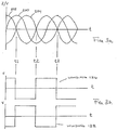
- Fig. 3a is a graph illustrating the relationship between certain voltages and currents of the charge equalization circuit 100 of Fig. 2 .
- the waveforms shown represent circuit operation when the charges on each battery 102 and 104 are substantially equal.
- An alternating current flowing through the resonant inductor 116 and resonant capacitor 118 is labeled 200.
- the inductance of the resonant inductor 116 and capacitance of the resonant capacitor 120 define a resonant frequency and the alternating current 200 substantially matches the resonant frequency.
- the voltage 202 across the resonant inductor 116 lags the alternating current 200 therethrough by 90 electrical degrees, while the voltage 204 across the resonant capacitor 118 leads the current therethrough by about 90 electrical degrees.
- Fig. 3b illustrates waveforms representing the bias voltages produced by the transistor drive circuit 133 for biasing transistors 130, 132 on and off.
- the waveforms of Fig. 3b are shown as square waves, although those skilled in the art will appreciate that in practice the waveforms are more complex.
- the voltage 202 across resonant inductor 116 is substantially negative (the plurality shown across inductor 116 in Fig. 1 being defined as positive). Accordingly, the voltage induced across winding 138 is positive, turning transistor 132 on. Transistor 130 is biased off at time t1. At time t2, the voltage 202 across resonant inductor 116 is substantially positive and the voltage induced across winding 136 is also positive, turning transistor 130 on. Transistor 132 is biased off at time t2.
- the alternating current 200 from time t1 through t2 flows into and out of battery 104, while the current 200 from time t2 through t3 flows into and out of battery 102.
- the charge on battery 102 is substantially equal to the charge on battery 104
- the amount of current flowing into and out of battery 104 is substantially equal.
- the amount of current flowing into and out of battery 102 is substantially equal.
- current 200 would include a DC component (i.e., a shift up or down) proportional to the difference in charge between batteries 102 and 104. Once the charge is equalized between batteries 102 and 104, current 200 would contain substantially no DC offset.
- transistors 130, 132 exhibit respective turn on threshold voltages below which the transistors will not turn on. Consequently, as the voltage across the resonant inductor 116 approaches zero volts (e.g., at time t1), the induced voltage across winding 136 approaches the threshold voltage of transistor 130. As transistor 130 begins to turn off, transistor 130 tends to limit the current 200 flowing (from left to right) in the resonant inductor 116. The resonant inductor 116 will oppose such a reduction in current and the voltage 202 across inductor 116 will change polarity. The induced voltage across winding 136 will also change polarity, thereby rapidly turning transistor 130 off.
- the bias signals produced by the transistor drive circuit 133 cause the resonant circuit 114 to operate at a frequency slightly above the resonant frequency, where the resonant circuit 114 will enjoy a dominant inductive characteristic.
- Fig. 4 illustrates a charge equalization circuit 300 according to an alternative embodiment of the present invention.
- the charge equalization circuit 300 includes substantially similar circuit components as shown in Fig. 2 but also includes diodes 150, 152 and capacitors 154, 156.
- Capacitors 154 and 156 operate as low impedance AC bypass circuits such that circulating resonant currents flow substantially through capacitors 154 and 156 rather than through batteries 102 and 104.
- batteries 102 and 104 do not exhibit losses and degradation from the circulating resonant currents.
- Diodes 150 and 152 are coupled from the intermediate node 122 of the resonant circuit 114 to the positive node 106 and negative node 108, respectively. Since the resonant circuit 114 operates near resonance with substantially no series resistance, the intermediate node 122 will tend to wing without bound.
- diodes 150 and 152 prevent the voltage at the intermediate node 122 from climbing substantially above the voltage on battery 102 or substantially below the voltage on battery 104.
- the charge equalization circuit 300 also includes a start-up circuit 160 which may be, for example, a push-to-start switch. Since the charge equalization circuit 300 can operate continuously, the start up circuit 160 need only be activated when the circuit is initially connected to the batteries 102, 104. Those skilled in the art will appreciate that the start up circuit 160 may enjoy continuous restart capability if a relaxation oscillator (for example employing an RC and DIAC configuration) is employed.
- a relaxation oscillator for example employing an RC and DIAC configuration
- the charge equalization circuit of the present invention be implemented on a circuit card which is disposed proximate to batteries 102 and 104.
- the number of batteries exceeds 2, for example, 3, 4, 5, 6 etc.
- one charge equalization circuit 300 may be employed for each pair of batteries. Such pairs overlap, so that complete equalization among all batteries is achieved. In n batteries are to be equalized, then 9n-10 equalization circuits are required.
- each charge equalization circuit is autonomous.
- the charge equalization circuits are thus distributed at the batteries for most convenient and safe operation.
Landscapes
- Engineering & Computer Science (AREA)
- Power Engineering (AREA)
- Manufacturing & Machinery (AREA)
- Chemical & Material Sciences (AREA)
- Chemical Kinetics & Catalysis (AREA)
- Electrochemistry (AREA)
- General Chemical & Material Sciences (AREA)
- Charge And Discharge Circuits For Batteries Or The Like (AREA)
- Secondary Cells (AREA)
Description
- The present invention relates to battery equalization techniques and, more particularly, to battery equalization apparatus employing resonant circuits.
- Batteries are typically connected in series such that a relatively large total voltage is available to drive a load. As it is desirable to utilize rechargeable batteries, battery charger circuits have been developed which charge all of the batteries in a series at one time.
- Care must be taken to charge each battery in the series fully without one battery being at a higher state of charge than another battery. If a difference exists between a relatively low charge on one battery with respect to the other batteries in the series, the total effective capacity of the series of batteries is reduced to the capacity of the battery having the low state of charge.
- Battery equalization circuits have been developed to ensure that all batteries in a series attain substantially the same state of charge.
U.S. Patent No. 5,479,083 to Brainard illustrates a conventionalbattery equalization circuit 10. The circuit is shown inFig. 1 herein. - The Brainard patent shows a series coupled pair of batteries B1, B2 which may be charged via a charging circuit 12. An equalization circuit includes a pair of series coupled transistors Q1 Q2 connected across the series coupled batteries. An inductor L is connected between the pair of transistors Q1, Q2 and the batteries B1, B2. An oscillator 14 produces gate drive signals to transistors Q1, Q2 such that they are alternately biased on and off for substantially equal durations. The inductor operates as a non-dissipative shunt that is alternately switched in parallel with each battery such that excessive charge on one battery is transferred to the other battery.
- Unfortunately, component tolerances within the Brainard
equalization circuit 10 will effect the degree of equalization achieved between the batteries. Indeed, tolerances which effect the duty cycle of the oscillator 14 and the resultant duty cycle presented by the transistors Q1, Q2 to the batteries will substantially effect the quality of equalization. Therefore, in order to obtain satisfactory equalization, measurements of the charge on each battery must be obtained and feed back to the oscillator to change the duty cycle as necessary (seeFig. 3 of the Brainard patent). -
U.S. Patent No. 5,710,504 to Pascual discloses a battery equalization circuit which does not require a feed back mechanism from each battery to achieve adequate equalization. However, the circuit of the Pascual patent requires that all switching devices within the circuit be synchronized no matter how many batteries are in the series combination. - When the number of series coupled batteries is relatively high and results in a high terminal voltage from the uppermost battery to the lowermost battery, the topology of the Pascual circuit may result in undesirable fault conditions.
- Turning to
Fig. 1 of the Pascual '504 patent, a plurality of series coupled batteries are shown and all switches 16 are synchronized via control lines 18 and control unit 12. Assuming that the total voltage from the uppermost battery to the lowermost battery is substantially large (e.g., 600 volts), a practical circuit must be designed to withstand a fault from the uppermost battery terminal to the lowermost battery terminal through the wiring of the equalization circuit. Often, the series coupled batteries may deliver many amps (approaching 1000 amps or more) making it difficult to design for surviving a fault and not damaging any of the batteries. - Accordingly, there is a need in the art for a new battery equalization circuit which is capable of autonomous operation (i.e., not requiring synchronization with other equalization circuits servicing the series coupled batteries) and does not require closed loop compensation to achieve satisfactory equalization.
- The battery equalization system of the present invention comprises at least first and second series connected batteries or battery cells and a battery equalization circuit that operates to equalize charge between said at least first and second series connected batteries or battery cells. Each battery or battery cell has a positive end and a negative end, where the positive end of the second battery or battery cell is coupled to the negative end of the first battery or battery cell at a common node. A resonant circuit has a first terminal connected to the common node and a second terminal, wherein the resonant circuit comprises a resonant inductor, a resonant capacitor connected in series with said resonant inductor and a bypass inductor connected in parallel to said resonant capacitor. A switching circuit comprises first and second switching transistors connected in a half bridge configuration, wherein the first transistor is connected between the positive end of the first battery or battery cell and the second terminal of the resonant circuit and the second transistor is connected between the second terminal of the resonant circuit and the negative end of the second battery or battery cell. A transistor drive circuit is adapted to produce first and second bias signals for turning the first and second switching transistors on and off, respectively. The switching circuit is adapted to alternately couple the resonant circuit in parallel with the first and second batteries or battery cells such that a DC current component flows between the first and second batteries or battery cells through the resonant circuit as a function of a charge imbalance therebetween.
- The resonant circuit is preferably a series resonant circuit including a resonant inductor coupled in series with a resonant capacitor. A DC bypass circuit is connected across the resonant capacitor such that a DC current component may flow therethrough and into one of the first and second batteries. The DC bypass circuit includes a bypass inductor, the bypass inductor preferably having an inductance substantially larger than the resonant inductor.
- The switching circuit includes first and second switching transistors coupled in a half bridge configuration from the positive node to the negative node and defining an output node therebetween. A transistor drive circuit is provided and adapted to produce first and second bias signals for turning the first and second switching transistors on and off, respectively. The transistor drive circuit is coupled to the resonant inductor such that the first and second bias signal are a function of a voltage across the resonant inductor.
- First and second windings wound on a common core of the resonant inductor or better with the resonant inductor of the resonant circuit such that the voltage across said resonant inductor induces voltages across said first and second windings are preferably included in the switching circuit, the first and second windings being wound oppositely with respect to one another such that the respective polarities of the induced polarities are opposite and said windings being coupled to bias terminals of the first and second switching transistors of the switching circuit, respectively. The voltage across the resonant inductor preferably induces proportional bias voltages for biasing the first and second switching transistors on and off in a positive feedback arrangement.
- First and second bypass capacitors may be provided, the first bypass capacitor coupled from the positive node to the common node and the second bypass capacitor coupled from the common node to the negative node. First and second bypass diodes may also be provided, the first diode being coupled with its anode from the intermediate node of the resonant circuit to the positive node, and the second diode being coupled with its cathode from the intermediate node of the resonant circuit to the negative node.
- Other objects, features, and advantages of the present invention will become apparent to those skilled in the art from the teachings herein taken in conjunction with the accompanying drawings.
- For the purpose of illustrating the invention, there are shown in drawing forms which are presently preferred, it being understood, however, that the present invention is not limited to the precise arrangements and instrumentalities shown.
-
Fig. 1 is a battery equalization circuit according to the prior art; -
Fig. 2 is a charge equalization circuit according to the present invention; -
Fig. 3a-3b are graphs illustrating certain waveforms present in the circuit ofFig. 2 ; and -
Fig. 4 is a schematic diagram illustrating additional details of a charge equalization circuit according to the present invention. - With reference to the accompanying drawings, wherein like numerals indicate like elements, there is shown in
Fig. 2 a circuit diagram illustrating acharge equalization circuit 100 according to the present invention. - The
charge equalization circuit 100 is operable to equalize the charge contained on respective series coupledbatteries Battery 102 includes a positive end coupled topositive node 106 and a negative end coupled to acommon node 110.Battery 104 includes a positive end coupled tocommon node 110 and a negative end coupled tonegative node 108. - Those skilled in the art will appreciate that the
charge equalization circuit 100 of the present invention need not operate with two completed batteries, such asbatteries battery 102 andbattery 104 may be thought of as individual series coupled cells within one battery. - The
charge equalization circuit 100 according to the present invention includes a switching circuit 112 connectable to thepositive node 106 and thenegative node 108 of the series coupled batteries and also includes aresonant circuit 114 connectable between the switching circuit 112 and thecommon node 110 ofbatteries - The
resonant circuit 114 is preferably a series resonant circuit including aresonant inductor 116 and aresonant capacitor 120 connected in series and defining anintermediate node 122 therebetween. Theresonant circuit 114 also preferably includes a DC bypass circuit connected across theresonant capacitor 118 such that DC current may flow through theresonant circuit 114 from the switching circuit 112 to thebatteries inductor 120 connected in a shunt configuration withresonant capacitor 118. - Those skilled in the art will appreciate from the teaching hereinbelow that
inductor 120 should have an inductance substantially larger than that ofresonant inductor 116, although inductance values forinductor 120 approaching (or lower than) that ofresonant inductor 116 are also contemplated as being within the scope of the invention. - The switching circuit 112 preferably includes a series coupled pair of
transistors positive node 106 to thenegative node 108, thetransistors output node 134 therebetween. The switching circuit 112 also preferably includes atransistor drive circuit 133 operable to produce bias signals for alternately biasingtransistors resonant inductor 116 such that the bias signals to thetransistors resonant inductor 116. -
Transistor drive circuit 133 preferably includeswindings resonant inductor 116 such that the voltage across theresonant inductor 116 induces voltages acrossrespective windings Windings - Preferably, transistors, 130, 132 are MOS-gated devices, with MOSFETs being most preferred.
Windings transistors - Reference is now made to
Fig. 3a which is a graph illustrating the relationship between certain voltages and currents of thecharge equalization circuit 100 ofFig. 2 . For simplicity, the waveforms shown represent circuit operation when the charges on eachbattery - An alternating current flowing through the
resonant inductor 116 andresonant capacitor 118 is labeled 200. The inductance of theresonant inductor 116 and capacitance of theresonant capacitor 120 define a resonant frequency and the alternating current 200 substantially matches the resonant frequency. - In general, the
voltage 202 across theresonant inductor 116 lags the alternating current 200 therethrough by 90 electrical degrees, while thevoltage 204 across theresonant capacitor 118 leads the current therethrough by about 90 electrical degrees. - Reference is now made to
Fig. 3b which illustrates waveforms representing the bias voltages produced by thetransistor drive circuit 133 for biasingtransistors Fig. 3b are shown as square waves, although those skilled in the art will appreciate that in practice the waveforms are more complex. - At time t1, the
voltage 202 acrossresonant inductor 116 is substantially negative (the plurality shown acrossinductor 116 inFig. 1 being defined as positive). Accordingly, the voltage induced across winding 138 is positive, turningtransistor 132 on.Transistor 130 is biased off at time t1. At time t2, thevoltage 202 acrossresonant inductor 116 is substantially positive and the voltage induced across winding 136 is also positive, turningtransistor 130 on.Transistor 132 is biased off at time t2. - With reference to
Fig. 3a , the alternating current 200 from time t1 through t2 flows into and out ofbattery 104, while the current 200 from time t2 through t3 flows into and out ofbattery 102. When the charge onbattery 102 is substantially equal to the charge onbattery 104, the amount of current flowing into and out of battery 104 (time t1 through t2) is substantially equal. Similarly, the amount of current flowing into and out of battery 102 (time t2 through t3) is substantially equal. - When the respective charges on
batteries bypass inductor 120 will shunt DC currents to one of the batteries until charge is equalized. Thus, current 200 would include a DC component (i.e., a shift up or down) proportional to the difference in charge betweenbatteries batteries - Those skilled in the art will appreciate that the waveforms illustrated in
Fig. 3a represent substantially ideal waveforms and that in practice slightly different waveforms will obtain. Indeed,transistors resonant inductor 116 approaches zero volts (e.g., at time t1), the induced voltage across winding 136 approaches the threshold voltage oftransistor 130. Astransistor 130 begins to turn off,transistor 130 tends to limit the current 200 flowing (from left to right) in theresonant inductor 116. Theresonant inductor 116 will oppose such a reduction in current and thevoltage 202 acrossinductor 116 will change polarity. The induced voltage across winding 136 will also change polarity, thereby rapidly turningtransistor 130 off. - Those skilled in the art will appreciate that the
voltage 202 acrossresonant inductor 116 is fed back to transistor drive circuit 133 (e.g., via winding 136) and introduces positive feedback in turningtransistor 130 off. A similar analysis obtains with respective to winding 138 andtransistor 132 at time t2. - In a practical circuit, therefore, the bias signals produced by the
transistor drive circuit 133 cause theresonant circuit 114 to operate at a frequency slightly above the resonant frequency, where theresonant circuit 114 will enjoy a dominant inductive characteristic. - Reference is now made to
Fig. 4 which illustrates acharge equalization circuit 300 according to an alternative embodiment of the present invention. Thecharge equalization circuit 300 includes substantially similar circuit components as shown inFig. 2 but also includesdiodes capacitors Capacitors capacitors batteries batteries -
Diodes intermediate node 122 of theresonant circuit 114 to thepositive node 106 andnegative node 108, respectively. Since theresonant circuit 114 operates near resonance with substantially no series resistance, theintermediate node 122 will tend to wing without bound. Advantageously,diodes intermediate node 122 from climbing substantially above the voltage onbattery 102 or substantially below the voltage onbattery 104. - The
charge equalization circuit 300 also includes a start-upcircuit 160 which may be, for example, a push-to-start switch. Since thecharge equalization circuit 300 can operate continuously, the start upcircuit 160 need only be activated when the circuit is initially connected to thebatteries circuit 160 may enjoy continuous restart capability if a relaxation oscillator (for example employing an RC and DIAC configuration) is employed. - It is most preferred that the charge equalization circuit of the present invention be implemented on a circuit card which is disposed proximate to
batteries charge equalization circuit 300 may be employed for each pair of batteries. Such pairs overlap, so that complete equalization among all batteries is achieved. In n batteries are to be equalized, then 9n-10 equalization circuits are required. - Advantageously, no synchronization or other control signals need be shared between charge equalization circuits for other pairs of batteries (i.e., each charge equalization circuit is autonomous). The charge equalization circuits are thus distributed at the batteries for most convenient and safe operation.
- Although the present invention has been described in relation to particular embodiments thereof, many other variations and modifications and other uses will become apparent to those skilled in the art. It is preferred, therefore, that the present invention be limited not by the specific disclosure herein, but only by the appended claims.
Claims (13)
- A battery equalization system comprising at least first (102) and second (104) series connected batteries or battery cells and a battery equalization circuit (100) for equalizing charge between said at least first (102) and second (104) series connected batteries or battery cells, each battery or battery cell (102, 104) including a positive end and a negative end, where the positive end of the second battery or battery cell (104) is coupled to the negative end of the first battery or battery cell (102) at a common node (110), the battery equalization circuit (100) comprising:a resonant circuit (114) having a first terminal connected to the common node (110) and a second terminal, wherein the resonant circuit (114) comprises a resonant inductor (116), a resonant capacitor (118) connected in series with said resonant inductor (116) and a bypass inductor (120) connected in parallel to said resonant capacitor (118),a switching circuit (112) comprising first (130) and second (132) switching transistors connected in a half bridge configuration, wherein the first transistor (130) is connected between the positive end of the first battery or battery cell (102) and the second terminal of the resonant circuit (114) and the second transistor (132) is connected between the second terminal of the resonant circuit (114) and the negative end of the second battery or battery cell (104); anda transistor drive circuit (133) adapted to produce first and second bias signals for turning the first and second switching transistors (130, 132) on and off, respectively, wherein the transistor drive circuit (133) is coupled to the resonant inductor (116) such that the first and second bias signals are a function of a voltage across the resonant inductor (116); andwherein the switching circuit (112) is adapted to alternately couple the resonant circuit (114) in parallel with the first and second batteries or battery cells (102, 104) such that a DC current component flows between the first and second batteries or battery cells (102, 104) through the resonant circuit (114) as a function of a charge imbalance therebetween.
- The battery equalization system of claim 1, wherein the bypass inductor (120) has an inductance substantially larger than the resonant inductor (116).
- The battery equalization system of claim 1, wherein the transistor drive circuit (133) produces the first bias signal to (i) bias the first transistor (130) on and the second transistor (132) off when the voltage across the resonant inductor (116) is generally positive, (ii) bias the first transistor (130) off and the second transistor (132) on when the voltage across the resonant inductor (116) is generally negative.
- The battery equalization system of claim 3, wherein the transistor drive circuit (133) includes first (136) and second (138) windings wound on a common core with the resonant inductor (116) of the resonant circuit (114) such that the voltage across said resonant inductor (116) induces voltages across said first and second windings (136, 138), the first (136) and second (138) windings being wound oppositely with respect to one another such that the respective polarities of the induced polarities are opposite and said windings (136, 138) being coupled to bias terminals of the first and second switching transistors (130, 132) of the switching circuit (112), respectively.
- The battery equalization system of claim 4, wherein the first and second switching transistors (130, 132) are MOS gated transistors, each having gating terminals, the first and second windings (136, 138) being coupled to the respective gating terminals.
- The battery equalization system of claim 5, wherein the first and second switching transistors (130, 132) are MOSFETs, a source of the first switching transistor (130) being coupled to a drain of the second switching transistor (132) at the second terminal, the first and second windings (136, 138) being coupled from respective gates to sources of the first and second switching transistors (130, 132).
- The battery equalization system of claim 3, wherein the transistor drive circuit (133) is adapted such that the voltage across the resonant inductor (116) induces proportional bias voltages for biasing the first and second switching transistors (130, 132) on and off in a positive feedback arrangement.
- The battery equalization system of claim 7, wherein each switching transistor (130, 132) has a threshold voltage of a magnitude below which the switching transistor (130, 132) will be biased off, the positive feedback of the transistor drive circuit (133) operating such that as the magnitude of the voltage across the resonant inductor (116) approaches zero, one of the bias voltages approaches the respective threshold voltage tending to (i) bias the corresponding switching transistor (130, 132) off, (ii) cause reduced current through the resonant inductor (116), (iii) cause reversal of the voltage across the resonant inductor (116), and (iv) cause the bias voltage to fall below the respective threshold voltage and fully bias the corresponding switching transistor (130, 132) off.
- The battery equalization system of claim 8, wherein reactive values of the resonant inductor (116) and resonant capacitor (118) define a resonant frequency, the positive feedback of the transistor drive circuit (133) causing the current through, and the voltages across, the resonant inductor (116) and resonant capacitor (118) to exhibit a frequency slightly above the resonant frequency.
- The battery equalization of system of claim 1, further comprising first and second bypass capacitors, the first bypass capacitor coupled from the positive node to the common node (110) and the second bypass capacitor coupled from the common node (110) to the negative node.
- The battery equalization system of claim 10, wherein the first and second bypass capacitors have reactive values sufficient to shunt circulating currents from the resonant circuit from flowing in the respective batteries or battery cells.
- The battery equalization system of claim 1, further comprising first and second bypass diodes having respective anodes and cathodes, the first diode being coupled with its anode from the intermediate node of the resonant circuit to the positive node, and the second diode being coupled with its cathode from the intermediate node of the resonant circuit to the negative node, the first and second diodes preventing a voltage at the intermediate node from rising substantially above the first battery voltage or falling substantially below the second battery voltage.
- The battery equalization system of claim 1, wherein each of the first and second battery cells include two or more sub-cells forming the respective battery cell.
Applications Claiming Priority (2)
| Application Number | Priority Date | Filing Date | Title |
|---|---|---|---|
| US320689 | 1999-05-27 | ||
| US09/320,689 US6140800A (en) | 1999-05-27 | 1999-05-27 | Autonomous battery equalization circuit |
Publications (3)
| Publication Number | Publication Date |
|---|---|
| EP1056182A2 EP1056182A2 (en) | 2000-11-29 |
| EP1056182A3 EP1056182A3 (en) | 2001-05-09 |
| EP1056182B1 true EP1056182B1 (en) | 2017-11-29 |
Family
ID=23247502
Family Applications (1)
| Application Number | Title | Priority Date | Filing Date |
|---|---|---|---|
| EP00104666.3A Expired - Lifetime EP1056182B1 (en) | 1999-05-27 | 2000-03-03 | Autonomous battery equalization circuit |
Country Status (10)
| Country | Link |
|---|---|
| US (1) | US6140800A (en) |
| EP (1) | EP1056182B1 (en) |
| JP (1) | JP4136274B2 (en) |
| KR (1) | KR100690039B1 (en) |
| CN (1) | CN1255917C (en) |
| AR (1) | AR029352A1 (en) |
| BR (1) | BR0001656A (en) |
| CA (1) | CA2309419C (en) |
| MX (1) | MXPA00005259A (en) |
| TW (1) | TW461128B (en) |
Families Citing this family (73)
| Publication number | Priority date | Publication date | Assignee | Title |
|---|---|---|---|---|
| US6452363B1 (en) | 2000-12-28 | 2002-09-17 | C. E. Niehoff & Co. | Multiple battery charge equalizer |
| TW501326B (en) * | 2001-01-10 | 2002-09-01 | Tai-He Yang | Electric equipment with backup battery-stand powered by host machine power source |
| US6653813B2 (en) * | 2002-03-21 | 2003-11-25 | Thomson Licensing, S.A. | Apparatus and method for the power management of operatively connected modular devices |
| WO2003100939A2 (en) * | 2002-05-20 | 2003-12-04 | Good Ideas Llc | Ultracapacitor balancing circuit |
| US6841971B1 (en) | 2002-05-29 | 2005-01-11 | Alpha Technologies, Inc. | Charge balancing systems and methods |
| US6771045B1 (en) * | 2002-09-05 | 2004-08-03 | Ise Corporation | Systems and methods for battery charging and equalization |
| US7378818B2 (en) * | 2002-11-25 | 2008-05-27 | Tiax Llc | Bidirectional power converter for balancing state of charge among series connected electrical energy storage units |
| WO2004097868A2 (en) * | 2003-04-25 | 2004-11-11 | Maxwell Technologies, Inc. | Charge balancing circuit for double-layer capacitors |
| US6806686B1 (en) | 2003-04-25 | 2004-10-19 | Maxwell Technologies, Inc. | Charge balancing circuit |
| US6985799B2 (en) | 2003-05-13 | 2006-01-10 | Bae Systems Controls, Inc. | Energy storage modules and management system |
| US7036028B2 (en) | 2003-05-13 | 2006-04-25 | Bae Systems Controls, Inc. | Power management system including a variable voltage link |
| US7342768B2 (en) * | 2004-02-17 | 2008-03-11 | Cooper Technologies Company | Active balancing modular circuits |
| US20060097700A1 (en) * | 2004-11-10 | 2006-05-11 | Eaglepicher Technologies, Llc | Method and system for cell equalization with charging sources and shunt regulators |
| US20060097697A1 (en) * | 2004-11-10 | 2006-05-11 | Eaglepicher Technologies, Llc | Method and system for cell equalization with switched charging sources |
| US7928691B2 (en) * | 2004-11-10 | 2011-04-19 | EaglePicher Technologies | Method and system for cell equalization with isolated charging sources |
| CN100356620C (en) * | 2005-01-10 | 2007-12-19 | 财团法人工业技术研究院 | Hierarchical battery potential balance device |
| CN100358212C (en) * | 2005-04-05 | 2007-12-26 | 苏州星恒电源有限公司 | Battery equalization method and battery equalization circuit |
| KR100831160B1 (en) * | 2005-04-15 | 2008-05-20 | 주식회사 엘지화학 | Switching circuit for balancing battery cells |
| US8058844B2 (en) * | 2006-05-31 | 2011-11-15 | Aeroflex Plainview, Inc. | Low-power battery system |
| US7786701B2 (en) * | 2006-05-31 | 2010-08-31 | Aeroflex Plainview, Inc. | Compensation for parasitic resistance in battery monitoring |
| DE102006033171A1 (en) | 2006-07-18 | 2008-01-24 | Robert Bosch Gmbh | Charging circuit for battery cells |
| KR101124800B1 (en) * | 2007-02-09 | 2012-03-23 | 한국과학기술원 | Charge Equalization Apparatus |
| US20100033128A1 (en) * | 2007-10-09 | 2010-02-11 | O2Micro, Inc. | Circuit and method for cell balancing |
| KR101220339B1 (en) * | 2007-10-16 | 2013-01-09 | 한국과학기술원 | Automatic Charge Equalization Method and Apparatus for Series Connected Battery String |
| DE102009000055A1 (en) * | 2009-01-07 | 2010-07-08 | Robert Bosch Gmbh | Battery cell balancing |
| US8493028B2 (en) | 2009-04-03 | 2013-07-23 | Marvell World Trade Ltd. | Power management circuit for rechargeable battery stack |
| US9397508B2 (en) * | 2009-05-22 | 2016-07-19 | Intersil Americas LLC | System and method for cell balancing and charging using a serially coupled inductor and capacitor |
| US8541980B2 (en) * | 2009-05-22 | 2013-09-24 | Intersil Americas LLC | System and method for cell balancing and charging |
| ES2361477B1 (en) * | 2009-06-08 | 2012-05-11 | Bozidar Konjevic | GENERATION OF ELECTRICAL ENERGY BY RESIDANCE IN BIDIRECTIONAL SERIES. |
| CN102035010B (en) | 2009-09-29 | 2013-05-01 | 凹凸电子(武汉)有限公司 | Battery unit equalizing circuit and method |
| US8339100B2 (en) | 2009-09-29 | 2012-12-25 | O2Micro Inc | Systems and methods for cell balancing |
| EP2312724A1 (en) | 2009-10-19 | 2011-04-20 | 4ESys NV | A system and method for balancing energy storage devices |
| US8525478B2 (en) | 2010-01-06 | 2013-09-03 | Marvell World Trade Ltd. | Power management circuit of rechargeable battery stack |
| FR2956260B1 (en) * | 2010-02-05 | 2012-04-13 | Commissariat Energie Atomique | CHARGE BALANCING SYSTEM FOR BATTERIES |
| CN102823104B (en) * | 2010-02-05 | 2016-05-11 | 法国原子能源和替代能源委员会 | Charge equalization system for batteries |
| DE102010029427A1 (en) | 2010-05-28 | 2011-12-01 | Siemens Aktiengesellschaft | Energy storage device |
| JP5070319B2 (en) * | 2010-07-16 | 2012-11-14 | ビステオン グローバル テクノロジーズ インコーポレイテッド | Remaining capacity equalizing apparatus and method, and remaining capacity equalizing apparatus set |
| TWI405384B (en) * | 2010-10-08 | 2013-08-11 | Ship & Ocean Ind R & D Ct | Active type cell charging equalizing method for battery packs |
| US8723482B2 (en) * | 2010-11-04 | 2014-05-13 | Elite Power Solutions Llc | Battery unit balancing system |
| FR2969850B1 (en) * | 2010-12-22 | 2013-09-27 | IFP Energies Nouvelles | CONVERTER FOR BALANCING THE CELLS OF AN ELECTRIC BATTERY |
| BR112013018549A2 (en) | 2011-01-22 | 2016-11-22 | Alpha Tech Inc | load equalization systems and methods |
| JP5744598B2 (en) * | 2011-03-31 | 2015-07-08 | Evtd株式会社 | Balance correction device and power storage system |
| CN103094935B (en) * | 2011-10-28 | 2016-01-13 | 东莞钜威新能源有限公司 | A kind of battery equalizing circuit and metal-oxide-semiconductor switching circuit |
| CN103094934A (en) * | 2011-10-28 | 2013-05-08 | 东莞钜威新能源有限公司 | A battery balancing circuit |
| FR2986392B1 (en) * | 2012-01-31 | 2016-05-06 | Renault Sa | COMMUNICATION SYSTEM IN AN ELECTRIC BATTERY |
| JP5864320B2 (en) * | 2012-03-19 | 2016-02-17 | Evtd株式会社 | Balance correction device and power storage system |
| US9438060B2 (en) | 2012-12-26 | 2016-09-06 | Colorado Energy Research Technologies, LLC | Power recovery controller |
| US9325188B2 (en) | 2012-12-26 | 2016-04-26 | Colorado Energy Research Technologies, LLC | Power recovery controller |
| US9428069B2 (en) | 2012-12-26 | 2016-08-30 | Colorado Energy Research Technologies, LLC | Systems and methods for efficiently charging power recovery controller |
| EP2939324A1 (en) * | 2012-12-26 | 2015-11-04 | Colorado Energy Research Technologies, LLC | Power recovery controller |
| KR101450717B1 (en) * | 2013-01-18 | 2014-10-16 | 포항공과대학교 산학협력단 | Battery cell ballancing circuit using series resonant circuit |
| US9620969B2 (en) * | 2013-01-24 | 2017-04-11 | Mitsubishi Electric Corporation | Storage battery equalization device capable of charging battery pack including storage battery modules having different output voltages in short time |
| KR102205841B1 (en) * | 2014-04-28 | 2021-01-21 | 삼성전자주식회사 | Method and apparatus for estimating state of battery |
| TW201543785A (en) * | 2014-05-14 | 2015-11-16 | Fu-Zi Xu | Damping charging device |
| CN105044609B (en) * | 2015-07-09 | 2017-11-14 | 重庆长安汽车股份有限公司 | The method of testing and system of battery cell equalization function effect |
| KR101917913B1 (en) | 2015-07-23 | 2018-11-12 | 주식회사 엘지화학 | Apparatus for balancing battery stack |
| KR102124186B1 (en) * | 2015-10-01 | 2020-06-17 | 주식회사 엘지화학 | Apparatus for balancing battery stack |
| DE102015117744A1 (en) * | 2015-10-19 | 2017-04-20 | Dr. Ing. H.C. F. Porsche Aktiengesellschaft | battery system |
| EP3550695B1 (en) * | 2016-12-28 | 2024-02-14 | Honda Motor Co., Ltd. | Electric circuit and diagnosis method |
| WO2018134827A1 (en) * | 2017-01-23 | 2018-07-26 | B.G. Negev Technologies And Applications Ltd., At Ben-Gurion University | System for balancing a series of cells |
| JP7269892B2 (en) | 2017-06-14 | 2023-05-09 | ハダル, インコーポレイテッド | Systems and methods for reducing parasitic power losses from energy sources |
| US11724620B2 (en) * | 2018-07-05 | 2023-08-15 | Volvo Truck Corporation | Method of controlling a battery system in a vehicle |
| CN111786036A (en) * | 2019-04-04 | 2020-10-16 | 纳恩博(北京)科技有限公司 | Battery system and vehicle |
| CN110048494B (en) * | 2019-05-30 | 2023-05-12 | 广东工业大学 | A battery cell voltage active equalization system |
| CN110247447A (en) * | 2019-05-31 | 2019-09-17 | 北京交通大学 | Echelon utilizes the sync equalizing current control method of battery pack |
| JP7344435B2 (en) * | 2019-06-03 | 2023-09-14 | マツダ株式会社 | vehicle drive system |
| US11545841B2 (en) * | 2019-11-18 | 2023-01-03 | Semiconductor Components Industries, Llc | Methods and apparatus for autonomous balancing and communication in a battery system |
| CN112838624B (en) * | 2019-11-22 | 2024-02-06 | 圣邦微电子(北京)股份有限公司 | Power supply circuit |
| US11342776B2 (en) * | 2020-06-15 | 2022-05-24 | Magnetic Energy Charging, Inc. | Battery charger and method for charging a battery |
| US12483043B2 (en) * | 2021-01-13 | 2025-11-25 | Renesas Electronics America Inc. | Bi-directional active battery cell balancer and method for bi-directional cell balancing |
| DE102022200634A1 (en) * | 2022-01-20 | 2023-07-20 | Robert Bosch Gesellschaft mit beschränkter Haftung | Method and device for reducing voltage stresses on semiconductor components of an inverter |
| CN115085314B (en) * | 2022-06-24 | 2023-07-18 | 上海南麟电子股份有限公司 | Battery asynchronous boost charging control circuit, chip, system and method |
| US12308674B1 (en) * | 2024-01-19 | 2025-05-20 | Moment Energy Inc. | Active energy balancing for energy storage systems |
Citations (1)
| Publication number | Priority date | Publication date | Assignee | Title |
|---|---|---|---|---|
| US5710504A (en) * | 1996-05-20 | 1998-01-20 | The Board Of Trustees Of The University Of Illinois | Switched capacitor system for automatic battery equalization |
Family Cites Families (11)
| Publication number | Priority date | Publication date | Assignee | Title |
|---|---|---|---|---|
| US4079303A (en) * | 1976-07-28 | 1978-03-14 | The United States Of America As Represented By The United States Department Of Energy | Charging system and method for multicell storage batteries |
| US4502001A (en) * | 1983-07-19 | 1985-02-26 | Energy Development Associates, Inc. | Current balancing for battery strings |
| JPH088116B2 (en) * | 1988-07-01 | 1996-01-29 | トヨタ自動車株式会社 | Complete discharge method for equalization of metal / halogen battery and metal / halogen battery used for the same |
| US4949028A (en) * | 1988-10-18 | 1990-08-14 | Sure Power, Inc. | Multiple voltage battery charge balancing and load protecting device |
| US5003244A (en) * | 1989-05-09 | 1991-03-26 | Digital Equipment Corporation | Battery charger for charging a plurality of batteries |
| US4967136A (en) * | 1989-09-25 | 1990-10-30 | Prestolite Electric Incorporated | Battery equalization circuit for a dual voltage charging system |
| US5479083A (en) * | 1993-06-21 | 1995-12-26 | Ast Research, Inc. | Non-dissipative battery charger equalizer |
| DE4422409C2 (en) * | 1994-06-29 | 1996-07-11 | Fraunhofer Ges Forschung | Device for the exchange of charges between a plurality of energy stores or converters connected in series |
| US5594320A (en) * | 1994-09-09 | 1997-01-14 | Rayovac Corporation | Charge equalization of series connected cells or batteries |
| US5528122A (en) * | 1994-11-29 | 1996-06-18 | Ventron Corporation | Battery voltage equalizer circuit |
| US5742150A (en) * | 1996-09-16 | 1998-04-21 | Khuwatsamrit; Thakoengdet | Power supply and method of protecting batteries therein |
-
1999
- 1999-05-27 US US09/320,689 patent/US6140800A/en not_active Expired - Lifetime
-
2000
- 2000-03-03 EP EP00104666.3A patent/EP1056182B1/en not_active Expired - Lifetime
- 2000-03-17 KR KR1020000013692A patent/KR100690039B1/en not_active Expired - Fee Related
- 2000-04-12 AR ARP000101691A patent/AR029352A1/en active IP Right Grant
- 2000-04-19 BR BR0001656-0A patent/BR0001656A/en not_active Application Discontinuation
- 2000-05-22 TW TW089109828A patent/TW461128B/en not_active IP Right Cessation
- 2000-05-25 CA CA002309419A patent/CA2309419C/en not_active Expired - Lifetime
- 2000-05-26 MX MXPA00005259A patent/MXPA00005259A/en active IP Right Grant
- 2000-05-29 JP JP2000158796A patent/JP4136274B2/en not_active Expired - Fee Related
- 2000-05-29 CN CNB001179276A patent/CN1255917C/en not_active Expired - Lifetime
Patent Citations (1)
| Publication number | Priority date | Publication date | Assignee | Title |
|---|---|---|---|---|
| US5710504A (en) * | 1996-05-20 | 1998-01-20 | The Board Of Trustees Of The University Of Illinois | Switched capacitor system for automatic battery equalization |
Also Published As
| Publication number | Publication date |
|---|---|
| JP2001008374A (en) | 2001-01-12 |
| KR20010014604A (en) | 2001-02-26 |
| BR0001656A (en) | 2001-03-13 |
| AR029352A1 (en) | 2003-06-25 |
| CA2309419A1 (en) | 2000-11-27 |
| JP4136274B2 (en) | 2008-08-20 |
| MXPA00005259A (en) | 2003-04-22 |
| KR100690039B1 (en) | 2007-03-08 |
| CA2309419C (en) | 2007-05-22 |
| CN1255917C (en) | 2006-05-10 |
| TW461128B (en) | 2001-10-21 |
| CN1275829A (en) | 2000-12-06 |
| EP1056182A3 (en) | 2001-05-09 |
| EP1056182A2 (en) | 2000-11-29 |
| US6140800A (en) | 2000-10-31 |
Similar Documents
| Publication | Publication Date | Title |
|---|---|---|
| CA2309419C (en) | Autonomous battery equalization circuit | |
| EP1107418B1 (en) | Magnetically coupled autonomous battery equalization circuit | |
| US11532987B2 (en) | Power conversion circuit, power conversion system and power chip | |
| US5982143A (en) | Battery equalization circuit with ramp converter and selective outputs | |
| US9318900B2 (en) | Power management system | |
| US11290027B1 (en) | Wireless charging receiver circuit and chip, and wireless charging receiver | |
| EP1186094B1 (en) | Method and apparatus for converting a dc voltage to an ac voltage | |
| US5666041A (en) | Battery equalization circuit with ramp converter | |
| EP3029801B1 (en) | System and method for cell balancing and charging using a serially coupled inductor and capacitor | |
| US8269455B2 (en) | Charge balancing system | |
| US20080030165A1 (en) | Method and Device for Supplying a Charge with Electric Energy Recovery | |
| US6906497B2 (en) | Enabling circuit for avoiding negative voltage transients | |
| US5798630A (en) | Switching power circuit to supply electric-vehicle battery charger with high-frequency power | |
| US7944188B1 (en) | Power converter circuits having bipolar outputs and bipolar inputs | |
| US6949912B2 (en) | Enabling circuit for avoiding negative voltage transients | |
| US4899270A (en) | DC-to-DC power supply including an energy transferring snubber circuit | |
| US20050281057A1 (en) | Holdover circuit for a power converter using a bi-directional switching regulator | |
| US6909617B1 (en) | Zero-voltage-switched, full-bridge, phase-shifted DC-DC converter with improved light/no-load operation | |
| EP1081824A2 (en) | A method and an apparatus for equalising the voltages over the capacitors in a series connection of capacitors during charging and discharging | |
| US6911746B2 (en) | Signal and power transformer coupling arrangements | |
| US20240429538A1 (en) | Battery pack, power tool system, synchronous rectification control circuit and switch power supply | |
| SE442076B (en) | PROCEDURE AND DEVICE FOR OPERATION OF POWER CONDENSERS FOR COMPENSATION OF REACTIVE DRUMS | |
| SU1665478A1 (en) | Dc voltage converter | |
| SU1367112A1 (en) | D.c.to d.c. voltage converter | |
| SU782092A1 (en) | Ac-to-dc converter |
Legal Events
| Date | Code | Title | Description |
|---|---|---|---|
| PUAI | Public reference made under article 153(3) epc to a published international application that has entered the european phase |
Free format text: ORIGINAL CODE: 0009012 |
|
| AK | Designated contracting states |
Kind code of ref document: A2 Designated state(s): DE FR GB IT NL SE |
|
| AX | Request for extension of the european patent |
Free format text: AL;LT;LV;MK;RO;SI |
|
| PUAL | Search report despatched |
Free format text: ORIGINAL CODE: 0009013 |
|
| AK | Designated contracting states |
Kind code of ref document: A3 Designated state(s): AT BE CH CY DE DK ES FI FR GB GR IE IT LI LU MC NL PT SE |
|
| AX | Request for extension of the european patent |
Free format text: AL;LT;LV;MK;RO;SI |
|
| RAP1 | Party data changed (applicant data changed or rights of an application transferred) |
Owner name: BAE SYSTEMS CONTROLS, INC. |
|
| 17P | Request for examination filed |
Effective date: 20011109 |
|
| AKX | Designation fees paid |
Free format text: DE FR GB IT NL SE |
|
| 17Q | First examination report despatched |
Effective date: 20101126 |
|
| RAP1 | Party data changed (applicant data changed or rights of an application transferred) |
Owner name: BAE SYSTEMS CONTROLS INC. |
|
| GRAP | Despatch of communication of intention to grant a patent |
Free format text: ORIGINAL CODE: EPIDOSNIGR1 |
|
| INTG | Intention to grant announced |
Effective date: 20170613 |
|
| GRAS | Grant fee paid |
Free format text: ORIGINAL CODE: EPIDOSNIGR3 |
|
| GRAA | (expected) grant |
Free format text: ORIGINAL CODE: 0009210 |
|
| AK | Designated contracting states |
Kind code of ref document: B1 Designated state(s): DE FR GB IT NL SE |
|
| REG | Reference to a national code |
Ref country code: GB Ref legal event code: FG4D |
|
| REG | Reference to a national code |
Ref country code: DE Ref legal event code: R096 Ref document number: 60049752 Country of ref document: DE |
|
| REG | Reference to a national code |
Ref country code: NL Ref legal event code: FP |
|
| REG | Reference to a national code |
Ref country code: FR Ref legal event code: PLFP Year of fee payment: 19 |
|
| PG25 | Lapsed in a contracting state [announced via postgrant information from national office to epo] |
Ref country code: SE Free format text: LAPSE BECAUSE OF FAILURE TO SUBMIT A TRANSLATION OF THE DESCRIPTION OR TO PAY THE FEE WITHIN THE PRESCRIBED TIME-LIMIT Effective date: 20171129 |
|
| PGFP | Annual fee paid to national office [announced via postgrant information from national office to epo] |
Ref country code: IT Payment date: 20180322 Year of fee payment: 19 |
|
| REG | Reference to a national code |
Ref country code: DE Ref legal event code: R097 Ref document number: 60049752 Country of ref document: DE |
|
| PLBE | No opposition filed within time limit |
Free format text: ORIGINAL CODE: 0009261 |
|
| STAA | Information on the status of an ep patent application or granted ep patent |
Free format text: STATUS: NO OPPOSITION FILED WITHIN TIME LIMIT |
|
| 26N | No opposition filed |
Effective date: 20180830 |
|
| PGFP | Annual fee paid to national office [announced via postgrant information from national office to epo] |
Ref country code: FR Payment date: 20190325 Year of fee payment: 20 Ref country code: DE Payment date: 20190327 Year of fee payment: 20 |
|
| PGFP | Annual fee paid to national office [announced via postgrant information from national office to epo] |
Ref country code: NL Payment date: 20190326 Year of fee payment: 20 |
|
| PGFP | Annual fee paid to national office [announced via postgrant information from national office to epo] |
Ref country code: GB Payment date: 20190404 Year of fee payment: 20 |
|
| PG25 | Lapsed in a contracting state [announced via postgrant information from national office to epo] |
Ref country code: IT Free format text: LAPSE BECAUSE OF NON-PAYMENT OF DUE FEES Effective date: 20190303 |
|
| REG | Reference to a national code |
Ref country code: DE Ref legal event code: R071 Ref document number: 60049752 Country of ref document: DE |
|
| REG | Reference to a national code |
Ref country code: GB Ref legal event code: PE20 Expiry date: 20200302 |
|
| PG25 | Lapsed in a contracting state [announced via postgrant information from national office to epo] |
Ref country code: GB Free format text: LAPSE BECAUSE OF EXPIRATION OF PROTECTION Effective date: 20200302 |
|
| REG | Reference to a national code |
Ref country code: NL Ref legal event code: MK Effective date: 20200302 |