EP1056125A2 - Lead germanate ferroelectric structure with multi-layered electrode - Google Patents
Lead germanate ferroelectric structure with multi-layered electrode Download PDFInfo
- Publication number
- EP1056125A2 EP1056125A2 EP00304385A EP00304385A EP1056125A2 EP 1056125 A2 EP1056125 A2 EP 1056125A2 EP 00304385 A EP00304385 A EP 00304385A EP 00304385 A EP00304385 A EP 00304385A EP 1056125 A2 EP1056125 A2 EP 1056125A2
- Authority
- EP
- European Patent Office
- Prior art keywords
- electrode
- pgo
- approximately
- film
- range
- Prior art date
- Legal status (The legal status is an assumption and is not a legal conclusion. Google has not performed a legal analysis and makes no representation as to the accuracy of the status listed.)
- Granted
Links
Images


Classifications
-
- H—ELECTRICITY
- H10—SEMICONDUCTOR DEVICES; ELECTRIC SOLID-STATE DEVICES NOT OTHERWISE PROVIDED FOR
- H10D—INORGANIC ELECTRIC SEMICONDUCTOR DEVICES
- H10D1/00—Resistors, capacitors or inductors
- H10D1/60—Capacitors
- H10D1/68—Capacitors having no potential barriers
- H10D1/682—Capacitors having no potential barriers having dielectrics comprising perovskite structures
- H10D1/684—Capacitors having no potential barriers having dielectrics comprising perovskite structures the dielectrics comprising multiple layers, e.g. comprising buffer layers, seed layers or gradient layers
-
- H—ELECTRICITY
- H10—SEMICONDUCTOR DEVICES; ELECTRIC SOLID-STATE DEVICES NOT OTHERWISE PROVIDED FOR
- H10D—INORGANIC ELECTRIC SEMICONDUCTOR DEVICES
- H10D1/00—Resistors, capacitors or inductors
- H10D1/01—Manufacture or treatment
- H10D1/041—Manufacture or treatment of capacitors having no potential barriers
- H10D1/042—Manufacture or treatment of capacitors having no potential barriers using deposition processes to form electrode extensions
-
- H—ELECTRICITY
- H10—SEMICONDUCTOR DEVICES; ELECTRIC SOLID-STATE DEVICES NOT OTHERWISE PROVIDED FOR
- H10D—INORGANIC ELECTRIC SEMICONDUCTOR DEVICES
- H10D1/00—Resistors, capacitors or inductors
- H10D1/60—Capacitors
- H10D1/68—Capacitors having no potential barriers
- H10D1/692—Electrodes
- H10D1/696—Electrodes comprising multiple layers, e.g. comprising a barrier layer and a metal layer
-
- H—ELECTRICITY
- H10—SEMICONDUCTOR DEVICES; ELECTRIC SOLID-STATE DEVICES NOT OTHERWISE PROVIDED FOR
- H10D—INORGANIC ELECTRIC SEMICONDUCTOR DEVICES
- H10D84/00—Integrated devices formed in or on semiconductor substrates that comprise only semiconducting layers, e.g. on Si wafers or on GaAs-on-Si wafers
- H10D84/80—Integrated devices formed in or on semiconductor substrates that comprise only semiconducting layers, e.g. on Si wafers or on GaAs-on-Si wafers characterised by the integration of at least one component covered by groups H10D12/00 or H10D30/00, e.g. integration of IGFETs
-
- H—ELECTRICITY
- H10—SEMICONDUCTOR DEVICES; ELECTRIC SOLID-STATE DEVICES NOT OTHERWISE PROVIDED FOR
- H10P—GENERIC PROCESSES OR APPARATUS FOR THE MANUFACTURE OR TREATMENT OF DEVICES COVERED BY CLASS H10
- H10P14/00—Formation of materials, e.g. in the shape of layers or pillars
- H10P14/60—Formation of materials, e.g. in the shape of layers or pillars of insulating materials
- H10P14/63—Formation of materials, e.g. in the shape of layers or pillars of insulating materials characterised by the formation processes
- H10P14/6302—Non-deposition formation processes
- H10P14/6304—Formation by oxidation, e.g. oxidation of the substrate
- H10P14/6314—Formation by oxidation, e.g. oxidation of the substrate of a metallic layer
-
- H—ELECTRICITY
- H10—SEMICONDUCTOR DEVICES; ELECTRIC SOLID-STATE DEVICES NOT OTHERWISE PROVIDED FOR
- H10P—GENERIC PROCESSES OR APPARATUS FOR THE MANUFACTURE OR TREATMENT OF DEVICES COVERED BY CLASS H10
- H10P14/00—Formation of materials, e.g. in the shape of layers or pillars
- H10P14/60—Formation of materials, e.g. in the shape of layers or pillars of insulating materials
- H10P14/63—Formation of materials, e.g. in the shape of layers or pillars of insulating materials characterised by the formation processes
- H10P14/6326—Deposition processes
- H10P14/6328—Deposition from the gas or vapour phase
- H10P14/6329—Deposition from the gas or vapour phase using physical ablation of a target, e.g. physical vapour deposition or pulsed laser deposition
-
- H—ELECTRICITY
- H10—SEMICONDUCTOR DEVICES; ELECTRIC SOLID-STATE DEVICES NOT OTHERWISE PROVIDED FOR
- H10P—GENERIC PROCESSES OR APPARATUS FOR THE MANUFACTURE OR TREATMENT OF DEVICES COVERED BY CLASS H10
- H10P14/00—Formation of materials, e.g. in the shape of layers or pillars
- H10P14/60—Formation of materials, e.g. in the shape of layers or pillars of insulating materials
- H10P14/63—Formation of materials, e.g. in the shape of layers or pillars of insulating materials characterised by the formation processes
- H10P14/6326—Deposition processes
- H10P14/6328—Deposition from the gas or vapour phase
- H10P14/6334—Deposition from the gas or vapour phase using decomposition or reaction of gaseous or vapour phase compounds, i.e. chemical vapour deposition
-
- H—ELECTRICITY
- H10—SEMICONDUCTOR DEVICES; ELECTRIC SOLID-STATE DEVICES NOT OTHERWISE PROVIDED FOR
- H10P—GENERIC PROCESSES OR APPARATUS FOR THE MANUFACTURE OR TREATMENT OF DEVICES COVERED BY CLASS H10
- H10P14/00—Formation of materials, e.g. in the shape of layers or pillars
- H10P14/60—Formation of materials, e.g. in the shape of layers or pillars of insulating materials
- H10P14/63—Formation of materials, e.g. in the shape of layers or pillars of insulating materials characterised by the formation processes
- H10P14/6326—Deposition processes
- H10P14/6349—Deposition of epitaxial materials
-
- H—ELECTRICITY
- H10—SEMICONDUCTOR DEVICES; ELECTRIC SOLID-STATE DEVICES NOT OTHERWISE PROVIDED FOR
- H10P—GENERIC PROCESSES OR APPARATUS FOR THE MANUFACTURE OR TREATMENT OF DEVICES COVERED BY CLASS H10
- H10P14/00—Formation of materials, e.g. in the shape of layers or pillars
- H10P14/60—Formation of materials, e.g. in the shape of layers or pillars of insulating materials
- H10P14/69—Inorganic materials
- H10P14/692—Inorganic materials composed of oxides, glassy oxides or oxide-based glasses
- H10P14/6938—Inorganic materials composed of oxides, glassy oxides or oxide-based glasses the material containing at least one metal element, e.g. metal oxides, metal oxynitrides or metal oxycarbides
- H10P14/6939—Inorganic materials composed of oxides, glassy oxides or oxide-based glasses the material containing at least one metal element, e.g. metal oxides, metal oxynitrides or metal oxycarbides characterised by the metal
-
- H—ELECTRICITY
- H10—SEMICONDUCTOR DEVICES; ELECTRIC SOLID-STATE DEVICES NOT OTHERWISE PROVIDED FOR
- H10P—GENERIC PROCESSES OR APPARATUS FOR THE MANUFACTURE OR TREATMENT OF DEVICES COVERED BY CLASS H10
- H10P14/00—Formation of materials, e.g. in the shape of layers or pillars
- H10P14/60—Formation of materials, e.g. in the shape of layers or pillars of insulating materials
- H10P14/69—Inorganic materials
- H10P14/692—Inorganic materials composed of oxides, glassy oxides or oxide-based glasses
- H10P14/6938—Inorganic materials composed of oxides, glassy oxides or oxide-based glasses the material containing at least one metal element, e.g. metal oxides, metal oxynitrides or metal oxycarbides
- H10P14/69398—Inorganic materials composed of oxides, glassy oxides or oxide-based glasses the material containing at least one metal element, e.g. metal oxides, metal oxynitrides or metal oxycarbides the material having a perovskite structure, e.g. BaTiO3
Definitions
- the present invention is generally related to the fabrication of integrated circuits (ICs) and, more specifically, to the fabrication of a lead germanate ferroelectric structure having an electrode of layered noble metals.
- Platinum (Pt) and other noble metals are used in IC ferroelectric capacitors.
- the use of noble metals is motivated by their inherent chemical resistance. This property is especially desirable under high temperature oxygen annealing conditions, such as those seen in the fabrication of ferroelectric capacitors.
- chemical interaction between noble metals and ferroelectric materials such as perovskite metal oxides, is negligible.
- the above-mentioned noble metals are used as conductive electrode pairs separated by a ferroelectric material.
- One, or both of the electrodes are often connected to transistor electrodes, or to electrically conductive traces in the IC.
- these ferroelectric devices can be polarized in accordance with the voltage applied to the electrode, with the relationship between charge and voltage expressed in a hysteresis loop.
- the polarized ferroelectric device can be used to represent a "1" or a "0".
- These memory devices are often called ferro-RAM, or FeRAM.
- Ferroelectric devices are nonvolatile. That is, the device remains polarized even after power is removed from the IC in which the ferroelectric is imbedded.
- Pt perhaps the widely used noble metal
- the diffusion of oxygen through Pt results in the oxidation of the neighboring barrier and substrate material.
- the neighboring substrate material is silicon or silicon dioxide. Oxidation can result in poor adhesion between the Pt and neighboring layer. Oxidation can also interfere with the conductivity between neighboring substrate layers. Silicon substrates are especially susceptible to problems occurring as a result of oxygen diffusion.
- the end result may be a ferroelectric device with degraded memory properties. Alternately, the temperature of the IC annealing process must be limited to prevent the degradation of the ferroelectric device.
- Titanium (Ti), titanium oxide (TiO 2 ), and titanium nitride (TiN) layers have been interposed between a noble metal and silicon (Si) substrates to suppress the interdiffusion of oxygen.
- Ti layers are generally only effective below annealing temperatures of 600 degrees C. After a 600 degree C annealing, Pt diffuses through the Ti layer to react with silicon, forming a silicide product. Further, the Pt cannot stop the oxygen diffusion. After a high temperature annealing, a thin layer of silicon oxide may be formed on the silicon surface, which insulates contact between silicon and the electrode.
- Ir has also been used in attempts to solve the oxygen interdiffusion problem. Ir is chemically stable, having a high melting temperature. Compared to Pt, Ir is more resistant to oxygen diffusion. Further, even when oxidized, iridium oxide remains conductive. When layered next to Ti, the Ir/Ti barrier is very impervious to oxygen interdiffusion. However, Ir can diffuse through Ti. Like Pt, Ir is very reactive with silicon or silicon dioxide. Therefore, a bilayered Ir/Ti or Ir/TiN barrier is not an ideal barrier metal.
- Pb 5 Ge 3 O 11 is a promising ferroelectric material candidate for nonvolatile memory, such as one-transistor (1T) applications, because of its moderate polarization and relative low dielectric constant. But, this material is a low symmetry ferroelectric material, and it is widely believed that spontaneous polarization exists only along the c-axis. Furthermore, in the PbO-GeO 2 system, the stability range for the Pb 5 Ge 3 O 11 phase is very limited. Even a relatively small deviation in composition, or in growth temperature, can lead to the formation of other lead germanate (PGO) compounds, or phases. Therefore, successful use of this ferroelectric material is dependent upon deposition processes and the adjoining electrode material.
- PGO lead germanate
- a suitable bottom electrode is required for depositing useful lead germanate (Pb 5 Ge 3 O 11 ) ferroelectric thin films.
- the bottom electrode must have good adhesion with the substrate, good electrical conductivity, and good barrier properties with respect to oxygen and lead.
- a good bottom electrode must also improve the fatigue degradation, and reduce the leakage current, of the lead-based ferroelectric thin film. From the processing point of view, the bottom electrode should provide a preferred nucleation and growth surface for the c-axis oriented lead germanate (Pb 5 Ge 3 O 11 ) thin film at a relative low MOCVD temperature.
- Single-layer platinum is widely used as the bottom electrode in PZT and SBT based nonvolatile ferroelectric memories.
- oxygen and elements such as lead can easily diffuse through Pt and react with barrier layers (Ti, TiN) and/or the substrate (Si or SiO 2 ), all of which are susceptible to oxidation. Deleterious oxidation leads to bad adhesion with the substrate, a poor interface between platinum and ferroelectric layers, and a poor interface between platinum and the substrate layers.
- Metal oxide electrodes such as RuO 2 axe used for PZT based nonvolatile memory to improve the fatigue degradation. But RuO 2 electrodes cause an increase in the leakage current.
- An oxide/platinum double-layer electrode reduces the leakage current, and improves the barrier properties and hillock problem. However, the leakage current is still larger than that of using a single-layer platinum electrode. Further, a thicker oxide layer is formed, resulting in a higher sheet resistance.
- a ferroelectric device comprising a silicon substrate, a first electrode layer of Ir overlying the substrate, and a second electrode layer of Pt overlying the first electrode layer.
- the first and second electrode layers have a combined thickness of about 100 to 400 nm, and are used to improve adhesion, barrier properties, and the uniformity of the PGO film.
- a first barrier layer of IrO 2 overlies the second electrode layer, to improve the interface to PGO film, and limit the diffusion of oxygen into the first and seconds electrode layers.
- a lead germanate (PGO) film having a Pb 5 Ge 3 O 11 phase of about 10 to 100% overlies the first barrier layer.
- the PGO film is epitaxially grown Pb 5 Ge 3 O 11 phase. In this manner, a ferroelectric device is formed having low leakage current and a resistance to fatigue.
- a material such as Ti, Ta, TiN, TaN, or a ternary nitride including nitrogen and a refractory metal, such as TiSiN or TaSiN, having a thickness of about 10 to 100 nanometers (nm)
- the ferroelectric device forms a capacitor with the addition of a conductive film top electrode overlying the PGO film.
- the top electrode optionally comprises a third Pt electrode layer overlying the PGO film, and a fourth Ir electrode layer overlying the third electrode layer to form a second layered electrode.
- a third barrier layer is interposed between the PGO film and the third electrode layer to improve the interface with the underlying PGO film.
- Also provided is a method of forming a ferroelectric device on a substrate comprising the steps of:
- Step c1) includes annealing the first and second electrode layers to form a first barrier layer oxide overlying the second electrode layer.
- Step c1) includes using processes selected from the group consisting of PVD, CVD, and MOCVD to deposit a first barrier layer of IrO 2 .
- Step c1) includes forming IrO 2 in preparation for an MOCVD process in Step d), by preflowing oxygen at a flow rate in the range of approximately 2000 to 4000 sccm, at a growth chamber pressure of approximately 10 torr, a substrate temperature in the range of approximately 400 to 550 degrees C, for a duration of approximately 10 to 15 minutes, whereby the first barrier layer is formed in situ.
- Step d) When a capacitor is formed, further steps following Step d), of:
- Pb 5 Ge 3 O 11 phase PGO has a relative low dielectric constant of about 50, contrasted to 1000 for PZT, and 300 for SBT.
- a low dielectric constant is a key factor in lowering the programming voltage for one-transistor memory applications.
- Lead germanate is a low symmetry ferroelectric material. Spontaneous polarization occurs only along one axis (c-axis) at a value of around 3-5 ⁇ C/cm 2 . Its Curie temperature is around 177° C. Many methods have been used to grow lead germanate thick films, such as rapid-quenching, printing, thermal evaporation, flash-evaporation, pulsed excimer laser ablation, dc reactive sputtering, and sol gel.
- the present invention discloses the formation of a lead germanate thin film through metal organic chemical vapor deposition (MOCVD) on a Pt/Ir bottom electrode.
- MOCVD metal organic chemical vapor deposition
- the lead germanate thin films were grown on Pt/TiN/SiO 2 /Si, Ir/Ti/SiO 2 /Si and Pt/Ir/Ti/SiO 2 electrodes through MOCVD processes.
- a liquid delivery system was used to deliver [Pb(thd) 2 ] and [Ge(ETO) 4 ] precursors to the growth chamber.
- the temperature of the vaporizer was about 150-200° C.
- the molar ratio of [Pb(thd) 2 ] to [Ge(ETO) 4 ] was around 5:3 and the substrate temperature was about 400-600° C.
- the growth chamber pressure was varied from 2-20 torr.
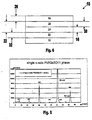
- Fig. 9 is a flowchart illustrating steps in a method of forming a ferroelectric device.
- Step 100 provides a substrate.
- Step 101 forms a second barrier layer overlying the substrate.
- the second barrier minimizes interdiffusion between the substrate and the electrode layers, while improving adhesion between the substrate and the electrode layers.
- the second barrier layer material is selected from the group consisting of consisting of Ti, Ta, TiN, TaN, and ternary nitrides including nitrogen and a refractory metal.
- the third element of the ternary group is selected from the group consisting of Si and Al.
- the second barrier thickness is in the range of approximately 10 to 100 nm.
- Step 102 forms a first electrode layer overlying the second barrier layer.
- Step 102 includes depositing Ir to a thickness in the range of approximately 50 to 200 nm.
- Step 104 forms a second electrode layer overlying the first electrode layer.
- Step 104 includes depositing Pt to a thickness in the range of approximately 10 to 200 nm.
- Steps 102 and 104 include depositing Ir and Pt to a combined thickness in the range of approximately 100 to 400 nm.
- Step. 102 and 104 include depositing the first and second electrode layers through processes selected from the group consisting of e-beam evaporation, CVD, PVD, and MOCVD, at a temperature in the range of approximately room temperature to 500 degrees C.
- Step 106 forms a first barrier layer overlying the second electrode layer.
- Step 106 includes forming the first barrier layer to a thickness in the range of approximately 5 to 50 nm.
- Step 108 is a product, a ferroelectric device where the barrier layers improve the interface to subsequently deposited layers, and limit the diffusion of oxygen into the first and second electrode layers.
- Step 106 includes annealing the first and second electrode layers in an oxygen ambient atmosphere to form a first barrier layer oxide overlying the second electrode layer.
- Step 106 includes using processes selected from the group consisting of PVD, CVD, and MOCVD to deposit a first barrier layer of IrO 2 .
- Step 110 forms a PGO layer overlying the first barrier layer.
- Step 110 includes depositing PGO film through MOCVD processes at a temperature in the range of approximately 400 to 550 degrees C, and a thickness in the range of approximately 50 to 500 nm.
- Step 110 includes the PGO film being in the range of approximately 10 to 100% Pb 5 Ge 3 O 11 phase, whereby the formation of smaller PGO crystal grains is encouraged.
- Step 110 includes the PGO film having a second, Pb 3 GeO 5 phase of PGO material, whereby the formation of larger PGO crystal grains is encouraged.
- the first and second phases are varied depended on desired ferroelectric and ferroelastic characteristics.
- Step 110 includes epitaxially growing a c-axis Pb 5 Ge 3 O 11 phase PGO material
- Step 110 includes forming the PGO film to a thickness in the range of approximately 50 to 500 nm.
- Step 112 forms a conductive film top electrode overlying the PGO film.
- Step 112 optionally includes sub-steps.
- Step 112a forms a third, Pt electrode layer overlying the PGO film; and
- Step 112b forms a fourth, Ir electrode layer overlying the third electrode layer, whereby a ferroelectric capacitor is formed.
- Step 110a forms a third barrier layer of IrO 2 overlying the PGO film formed in Step 110, whereby the interface between the PGO film and the third and fourth electrode layers is improved.
- Step 112b a further step follows Step 112b.
- Step 114 (not shown) anneals the third and fourth electrode layers in an oxygen ambient atmosphere.
- Step 110a occurs, in situ, simultaneously with the performance of Step 114.
- Step 110a occurs after Step 110, and before Step 112.
- Step 110a includes depositing IrO2 through deposition procedures selected from the group consisting of PVD, CVD, and MOCVD.
- Step 116 is a product, a capacitor having improved fatigue and leakage current properties.
- the present invention ferroelectric structure is simply and easily manufactured.
- the Pt/Ir double-layer is advantageously used with a lead germanate (Pb 5 Ge 3 O 11 ) thin film. Good adhesion to the substrate occurs, and the barrier properties with respect to oxygen and lead are good. Ferroelectric properties are improved without detriment to the leakage current by using this structure, because a thin IrO 2 layer is formed in situ, during the MOCVD lead germanate (Pb 5 Ge 3 O 11 ) thin film process.
- a Pt/Ir electrode a relatively low MOCVD processing temperature is required to achieve c-axis oriented lead germanate (Pb 5 Ge 3 O 11 ) thin film.
- the temperature range of MOCVD c-axis oriented lead germanate (Pb 5 Ge 3 O 11 ) thin film on top of Pt/Ir is 400-500° C. Further, a relatively large nucleation density is obtained, as compared to using single-layer iridium electrode. Therefore, the lead germanate (Pb 5 Ge 3 O 11 ) thin film has a smooth surface, a homogeneous microstructure, and homogeneous ferroelectric properties.
- ferroelectric structure is useful in the fabrication of nonvolatile memories, such as metal ferroelectric metal oxide silicon (MFMOS), metal ferroelectric metal silicon (MFMS), metal ferroelectric metal insulator silicon (MFMIS), transistors, capacitors, pyroelectric infrared sensors, optical displays, optical switches, piezoelectric transducers, and surface acoustic wave (SAW) devices.
- MMOS metal ferroelectric metal oxide silicon
- MFMS metal ferroelectric metal silicon
- MFMIS metal ferroelectric metal insulator silicon
- transistors capacitors
- pyroelectric infrared sensors optical displays
- optical switches optical switches
- piezoelectric transducers piezoelectric transducers
- SAW surface acoustic wave
Landscapes
- Semiconductor Memories (AREA)
- Non-Volatile Memory (AREA)
- Physical Vapour Deposition (AREA)
- Chemical Vapour Deposition (AREA)
Abstract
Description
Claims (39)
- A ferroelectric device comprising:a substrate;a first electrode layer including a noble metal overlying said substrate;a second electrode layer including a noble metal overlying said first electrode layer, whereby said first and second electrode layers improve adhesion, barrier properties, and the uniformity of subsequently deposited films;a first barrier layer overlying said second electrode layer, whereby said first barrier layer improves the interface to subsequently deposited layers, and limits the diffusion of oxygen into said first and second electrode layers; anda second barrier layer interposed between said substrate and said first electrode layer, whereby said second barrier layer minimizes interdiffusion between said substrate and said electrode layers, and adhesion between said substrate and said electrode layers is improved.
- A ferroelectric device as in claim 1 further comprising a lead germanate (PGO) film overlying said first barrier layer, whereby a ferroelectric device is formed having low leakage current and a resistance to fatigue.
- A ferroelectric device as in claim 1 or claim 2 in which said second barrier layer has a thickness in the range of approximately 10 to 100 nm.
- A ferroelectric device as in any preceding claim in which said second barrier layer material is selected from the group consisting of Ti, Ta, TiN, TaN, and ternary nitrides including nitrogen and a refractory metal.
- A ferroelectric device as in claim 2, wherein a capacitor is formed, further comprising:a conductive film top electrode overlying said PGO film.
- A ferroelectric device as in claim 5 in which said top electrode further comprises:a third electrode layer of Pt overlying said PGO film; anda fourth electrode layer of Ir overlying said third electrode layer,
whereby a second layered electrode is formed. - A ferroelectric device as in claim 6 further comprising:a third baffler layer of IrO2 interposed between said PGO film and said third electrode layer, whereby the interface between said PGO film and said third and fourth electrode layers is improved.
- A ferroelectric device as in any preceding claim in which said first electrode layer is Ir.
- A ferroelectric device as in any preceding claim in which said second electrode layer is Pt.
- A ferroelectric device as in claim 7 in which said first barrier material is IrO2.
- A ferroelectric device as in claim 2 in which said PGO film is in the range of approximately 10 to 100% Pb5Ge3O11 phase, whereby the formation of smaller PGO crystal grains is encouraged.
- A ferroelectric device as in claim 11 in which said PGO film includes a second, Pb3GeO5 phase of PGO material, whereby the formation of larger PGO crystal grains is encouraged.
- A ferroelectric device as in claim 11 in which said PGO film is epitaxially grown, c-axis Pb5Ge3O11 phase PGO material.
- A ferroelectric device as in claim 2 in which said PGO film has a thickness in the range of approximately 50 to 500 nm.
- A ferroelectric device as in any preceding claim in which said substrate is selected from the group of materials consisting of silicon, polysilicon, silicon dioxide, and silicon-germanium compounds.
- A ferroelectric device as in any preceding claim in which said first electrode layer has a thickness in the range of approximately 50 to 200 nm, and in which said second electrode layer has a thickness in the range of approximately 10 to 200 nm.
- A ferroelectric device as in claim 16 in which said first and second electrodes have a combined thickness in the range of approximately 100 to 400 nm.
- A ferroelectric device as in any preceding claim in which said first barrier layer has a thickness in the range of approximately 5 to 50 nm.
- A method of forming a ferroelectric device on a substrate comprising the steps of:a) forming a second barrier layer overlying the substrate;b) forming a first electrode layer overlying the second barrier layer;c) forming a second electrode layer overlying the first electrode layer; andd) forming a first barrier layer overlying the second electrode layer, whereby the first barrier layer improves the interface to subsequently deposited layers, and limits the diffusion of oxygen into the first and second electrode layers.
- A method as in claim 19 in which Step a) includes the second barrier layer material being selected from the group consisting of Ti, Ta, TiN, TaN, and ternary nitrides including nitrogen and a refractory metal, and in which the second barrier thickness is in the range of approximately 10 to 100 nm.
- A method as in claim 19 or claim 20 in which Step d) includes annealing the first and second electrode layers in an oxygen ambient atmosphere to form a first barrier layer oxide overlying the second electrode layer.
- A method as in claim 19 or claim 20 in which Step d) includes using processes selected from the group consisting of PVD, CVD, and MOCVD to deposit a first barrier layer of IrO2.
- A method as in any of claims 19 to 22 in which Step b) includes depositing Ir to a thickness in the range of approximately 50 to 200 nm.
- A method as in any of claims 19 to 23 in which Step c) includes depositing Pt to a thickness in the range of approximately 10 to 200 nm.
- A method as in any of claims 19 to 22 in which Steps b) and c) include depositing Ir and Pt to a combined thickness in the range of approximately 100 to 400 nm.
- A method as in any of claims 19 to 25 in which Steps b) and c) include depositing the first and second electrode layers through processes selected from the group consisting of e-beam evaporation, CVD, PVD, and MOCVD, at a temperature in the range of approximately room temperature to 500 degrees C.
- A method as in any of claims 19 to 26 in which Step d) includes forming the first barrier layer to a thickness in the range of approximately 5 to 50 nm.
- A method as in any of claims 19 to 27 comprising a further step, following Step d), of:e) forming a PGO film overlying the first barrier layer.
- A method as in claim 28 in which Step e) includes depositing PGO film through MOCVD processes at a temperature in the range of approximately 400 to 550 degrees C, and a thickness in the range of approximately 50 to 500 nm.
- A method as in claim 28 in which Step e) includes the PGO film being in the range of approximately 10 to 100% Pb5Ge3O11 phase, whereby the formation of smaller PGO crystal grains is encouraged.
- A method as in claim 28 in which Step e) includes the PGO film having a second, Pb3GeO5 phase of PGO material, whereby the formation of larger PGO crystal grains is encouraged.
- A method as in claim 28 in which Step e) includes epitaxially growing a c-axis Pb5Ge3O11 phase PGO material.
- A method as in claim 28 in which Step e) includes forming the PGO film to a thickness in the range of approximately 50 to 500 nm.
- A method as in claim 28 in which Step d) includes forming IrO2 in preparation for an MOCVD process in Step e), by pre-flowing oxygen at a flow rate in the range of approximately 2000 to 4000 sccm, at a pressure of approximately 2 to 20 torr, a substrate temperature in the range of approximately 400 to 550 degrees C, for a duration of approximately 5 to 15 minutes, whereby the first barrier layer is formed in situ.
- A method as in any of claims 28 to 34 wherein a capacitor is formed including a further step, following Step e), of:f) forming conductive film top electrode overlying the PGO film.
- A method as in claim 35 in which Step f) includes the sub-steps of:1) forming a third, Pt electrode layer overlying the PGO film; and2) forming a fourth, Ir electrode layer overlying the third electrode layer, whereby a ferroelectric capacitor is formed.
- A method as in claim 36 including a further step, following Step e), of:e1) forming a third barrier layer of IrO2 overlying the PGO film formed in Step e), whereby the interface between the PGO film and the third and fourth electrode layers is improved.
- A method as in claim 37 including a further step, following Step f), of:g) annealing the third and fourth electrode layers in an oxygen ambient atmosphere; andin which Step e1) occurs, in situ, simultaneously with the performance of Step g).
- A method as in claim 37 in which Step e1) occurs after Step e), and before Step f), and in which Step e1) includes depositing IrO2 through deposition procedures selected from the group consisting of PVD, CVD, and MOCVD.
Applications Claiming Priority (2)
| Application Number | Priority Date | Filing Date | Title |
|---|---|---|---|
| US317780 | 1981-11-03 | ||
| US09/317,780 US6420740B1 (en) | 1999-05-24 | 1999-05-24 | Lead germanate ferroelectric structure with multi-layered electrode |
Publications (3)
| Publication Number | Publication Date |
|---|---|
| EP1056125A2 true EP1056125A2 (en) | 2000-11-29 |
| EP1056125A3 EP1056125A3 (en) | 2003-08-06 |
| EP1056125B1 EP1056125B1 (en) | 2007-06-27 |
Family
ID=23235244
Family Applications (1)
| Application Number | Title | Priority Date | Filing Date |
|---|---|---|---|
| EP00304385A Expired - Lifetime EP1056125B1 (en) | 1999-05-24 | 2000-05-24 | Lead germanate ferroelectric structure with multi-layered electrode |
Country Status (6)
| Country | Link |
|---|---|
| US (2) | US6420740B1 (en) |
| EP (1) | EP1056125B1 (en) |
| JP (1) | JP3832617B2 (en) |
| KR (1) | KR100373079B1 (en) |
| DE (1) | DE60035311T2 (en) |
| TW (1) | TW494576B (en) |
Cited By (1)
| Publication number | Priority date | Publication date | Assignee | Title |
|---|---|---|---|---|
| US6586260B2 (en) * | 2001-03-28 | 2003-07-01 | Sharp Laboratories Of America, Inc. | Single c-axis PGO thin film electrodes having good surface smoothness and uniformity and methods for making the same |
Families Citing this family (22)
| Publication number | Priority date | Publication date | Assignee | Title |
|---|---|---|---|---|
| US20030001189A1 (en) * | 2000-02-24 | 2003-01-02 | Tetsuo Fujiwara | Ferroelectric capacitor and semiconductor device |
| DE10035423C1 (en) * | 2000-07-20 | 2001-11-22 | Infineon Technologies Ag | Semiconductor component with a layer sequence for converting acoustic or thermal signals and electrical voltage changes into one another and method for its production |
| US6503763B2 (en) * | 2001-03-27 | 2003-01-07 | Sharp Laboratories Of America, Inc. | Method of making MFMOS capacitors with high dielectric constant materials |
| US6960479B2 (en) * | 2001-07-20 | 2005-11-01 | Intel Corporation | Stacked ferroelectric memory device and method of making same |
| KR100476375B1 (en) * | 2002-12-27 | 2005-03-17 | 주식회사 하이닉스반도체 | Capacitor and method for fabricating nonvolatile device with the same |
| US6952364B2 (en) * | 2003-03-03 | 2005-10-04 | Samsung Electronics Co., Ltd. | Magnetic tunnel junction structures and methods of fabrication |
| KR100615600B1 (en) * | 2004-08-09 | 2006-08-25 | 삼성전자주식회사 | Highly Integrated Magnetic Ram Device and Manufacturing Method Thereof |
| JP4643196B2 (en) * | 2003-07-25 | 2011-03-02 | 三星電子株式会社 | Deposition method of metal compound film |
| NO20041733L (en) * | 2004-04-28 | 2005-10-31 | Thin Film Electronics Asa | Organic electronic circuit with functional interlayer and process for its manufacture. |
| JP2005347510A (en) * | 2004-06-03 | 2005-12-15 | Matsushita Electric Ind Co Ltd | Semiconductor device and manufacturing method thereof |
| US7267996B2 (en) * | 2004-08-20 | 2007-09-11 | Sharp Laboratories Of America, Inc. | Iridium etching for FeRAM applications |
| US7041511B2 (en) * | 2004-08-20 | 2006-05-09 | Sharp Laboratories Of America, Inc. | Pt/PGO etching process for FeRAM applications |
| US20060073613A1 (en) * | 2004-09-29 | 2006-04-06 | Sanjeev Aggarwal | Ferroelectric memory cells and methods for fabricating ferroelectric memory cells and ferroelectric capacitors thereof |
| US20060141225A1 (en) * | 2004-12-28 | 2006-06-29 | Borland William J | Oxygen doped firing of barium titanate on copper foil |
| US9305998B2 (en) * | 2013-02-11 | 2016-04-05 | Texas Instruments Incorporated | Adhesion of ferroelectric material to underlying conductive capacitor plate |
| US8809827B1 (en) * | 2013-03-13 | 2014-08-19 | International Business Machines Corporation | Thermally assisted MRAM with multilayer strap and top contact for low thermal conductivity |
| US9515251B2 (en) | 2014-04-09 | 2016-12-06 | International Business Machines Corporation | Structure for thermally assisted MRAM |
| JP6367152B2 (en) * | 2015-06-08 | 2018-08-01 | 東芝メモリ株式会社 | Storage device |
| JP6039026B1 (en) * | 2015-09-04 | 2016-12-07 | Dowaエレクトロニクス株式会社 | Manufacturing method of n-type ohmic electrode, n-type ohmic electrode, n-type electrode, and group III nitride semiconductor light emitting device |
| US10038092B1 (en) * | 2017-05-24 | 2018-07-31 | Sandisk Technologies Llc | Three-level ferroelectric memory cell using band alignment engineering |
| JP7200537B2 (en) * | 2018-08-21 | 2023-01-10 | 富士フイルムビジネスイノベーション株式会社 | Semiconductor substrate manufacturing method |
| US11916127B2 (en) | 2021-06-16 | 2024-02-27 | Taiwan Semiconductor Manufacturing Company, Ltd. | Multi-layer electrode to improve performance of ferroelectric memory device |
Family Cites Families (15)
| Publication number | Priority date | Publication date | Assignee | Title |
|---|---|---|---|---|
| EP0042009A1 (en) * | 1980-06-11 | 1981-12-23 | University of Illinois Foundation | Internal boundary layer ceramic compositions and process for their production |
| GB8802930D0 (en) | 1988-02-09 | 1988-03-09 | Plasmon Data Systems Uk Ltd | Improved data storage medium |
| US5005102A (en) * | 1989-06-20 | 1991-04-02 | Ramtron Corporation | Multilayer electrodes for integrated circuit capacitors |
| JP3197782B2 (en) * | 1994-04-29 | 2001-08-13 | インターナショナル・ビジネス・マシーンズ・コーポレ−ション | Semiconductor integrated circuit capacitor and its electrode structure |
| US5585300A (en) | 1994-08-01 | 1996-12-17 | Texas Instruments Incorporated | Method of making conductive amorphous-nitride barrier layer for high-dielectric-constant material electrodes |
| JP3279453B2 (en) | 1995-03-20 | 2002-04-30 | シャープ株式会社 | Non-volatile random access memory |
| JPH11511293A (en) * | 1995-06-07 | 1999-09-28 | サイメトリックス コーポレイション | Integrated circuit including a substrate and a wiring layer, and having a buffer layer between the substrate and the wiring layer |
| JP3504046B2 (en) * | 1995-12-05 | 2004-03-08 | 株式会社ルネサステクノロジ | Method for manufacturing semiconductor device |
| KR100246989B1 (en) | 1996-09-09 | 2000-03-15 | 김영환 | Method for forming capacitor of semiconductor device |
| US5807774A (en) * | 1996-12-06 | 1998-09-15 | Sharp Kabushiki Kaisha | Simple method of fabricating ferroelectric capacitors |
| US5790366A (en) * | 1996-12-06 | 1998-08-04 | Sharp Kabushiki Kaisha | High temperature electrode-barriers for ferroelectric and other capacitor structures |
| US6011284A (en) * | 1996-12-26 | 2000-01-04 | Sony Corporation | Electronic material, its manufacturing method, dielectric capacitor, nonvolatile memory and semiconductor device |
| US5932904A (en) * | 1997-03-07 | 1999-08-03 | Sharp Laboratories Of America, Inc. | Two transistor ferroelectric memory cell |
| US6107136A (en) * | 1998-08-17 | 2000-08-22 | Motorola Inc. | Method for forming a capacitor structure |
| US6410343B1 (en) * | 1999-04-28 | 2002-06-25 | Sharp Laboratories Of America, Inc. | C-axis oriented lead germanate film and deposition method |
-
1999
- 1999-05-24 US US09/317,780 patent/US6420740B1/en not_active Expired - Fee Related
-
2000
- 2000-05-24 EP EP00304385A patent/EP1056125B1/en not_active Expired - Lifetime
- 2000-05-24 DE DE60035311T patent/DE60035311T2/en not_active Expired - Lifetime
- 2000-05-24 KR KR10-2000-0028047A patent/KR100373079B1/en not_active Expired - Fee Related
- 2000-05-24 TW TW089110042A patent/TW494576B/en not_active IP Right Cessation
- 2000-05-24 JP JP2000153312A patent/JP3832617B2/en not_active Expired - Fee Related
-
2002
- 2002-07-15 US US10/196,503 patent/US6759250B2/en not_active Expired - Fee Related
Cited By (1)
| Publication number | Priority date | Publication date | Assignee | Title |
|---|---|---|---|---|
| US6586260B2 (en) * | 2001-03-28 | 2003-07-01 | Sharp Laboratories Of America, Inc. | Single c-axis PGO thin film electrodes having good surface smoothness and uniformity and methods for making the same |
Also Published As
| Publication number | Publication date |
|---|---|
| EP1056125A3 (en) | 2003-08-06 |
| JP2001007299A (en) | 2001-01-12 |
| TW494576B (en) | 2002-07-11 |
| EP1056125B1 (en) | 2007-06-27 |
| KR100373079B1 (en) | 2003-02-25 |
| DE60035311T2 (en) | 2008-02-28 |
| JP3832617B2 (en) | 2006-10-11 |
| US6420740B1 (en) | 2002-07-16 |
| US20020180045A1 (en) | 2002-12-05 |
| US6759250B2 (en) | 2004-07-06 |
| KR20000077404A (en) | 2000-12-26 |
| DE60035311D1 (en) | 2007-08-09 |
Similar Documents
| Publication | Publication Date | Title |
|---|---|---|
| US6420740B1 (en) | Lead germanate ferroelectric structure with multi-layered electrode | |
| US6288420B1 (en) | Composite iridium-metal-oxygen barrier structure with refractory metal companion barrier | |
| US6351006B1 (en) | Ferroelectric capacitor with means to prevent deterioration | |
| US20040232468A1 (en) | Barrier layers for protecting metal oxides from hydrogen degradation | |
| EP1054440A2 (en) | Composite iridium barrier structure with oxidized refractory metal companion barrier and method for its fabrication | |
| US6670668B2 (en) | Microelectronic structure, method for fabricating it and its use in a memory cell | |
| JP3435633B2 (en) | Thin film laminate, thin film capacitor, and method of manufacturing the same | |
| KR100378276B1 (en) | Insulating material, substrate covered with an insulating film, method of producing the same, and thin-film device | |
| US7514272B2 (en) | Method of manufacturing ferroelectric memory device | |
| US20080123243A1 (en) | Ferroelectric capacitor | |
| JP4164700B2 (en) | Ferroelectric memory and manufacturing method thereof | |
| JP3474352B2 (en) | Thin film capacitor and semiconductor device | |
| US6236113B1 (en) | Iridium composite barrier structure and method for same | |
| US7271054B2 (en) | Method of manufacturing a ferroelectric capacitor having RU1-XOX electrode | |
| US6812510B2 (en) | Ferroelectric capacitor, process for manufacturing thereof and ferroelectric memory | |
| US6297085B1 (en) | Method for manufacturing ferroelectric capacitor and method for manufacturing ferroelectric memory | |
| JP3353833B2 (en) | Semiconductor device and method of manufacturing the same | |
| US20080019075A1 (en) | Dielectric capacitor | |
| JPH11261028A (en) | Thin film capacitors | |
| JP2002334875A (en) | Vapor growth method for metal oxide dielectric film | |
| JP4928098B2 (en) | Method for manufacturing ferroelectric capacitor | |
| EP1077478A2 (en) | Method of making ferroelectric thin film, ferroelectric capacitor, ferroelectric memory and method for fabricating ferroelectric memory | |
| KR20010045568A (en) | Capacitor manufacturing method for preventing defect generation at subsequent annealing | |
| JP3400218B2 (en) | Dielectric capacitor | |
| KR100247924B1 (en) | Method of manufacturing capacitor improved diffusion barrier property |
Legal Events
| Date | Code | Title | Description |
|---|---|---|---|
| PUAI | Public reference made under article 153(3) epc to a published international application that has entered the european phase |
Free format text: ORIGINAL CODE: 0009012 |
|
| AK | Designated contracting states |
Kind code of ref document: A2 Designated state(s): AT BE CH CY DE DK ES FI FR GB GR IE IT LI LU MC NL PT SE |
|
| AX | Request for extension of the european patent |
Free format text: AL;LT;LV;MK;RO;SI |
|
| RIN1 | Information on inventor provided before grant (corrected) |
Inventor name: HSU, SHENG TENG Inventor name: LI, TINGKAI Inventor name: ZHANG, FENGYAN |
|
| PUAL | Search report despatched |
Free format text: ORIGINAL CODE: 0009013 |
|
| AK | Designated contracting states |
Designated state(s): AT BE CH CY DE DK ES FI FR GB GR IE IT LI LU MC NL PT SE |
|
| AX | Request for extension of the european patent |
Extension state: AL LT LV MK RO SI |
|
| RIC1 | Information provided on ipc code assigned before grant |
Ipc: 7H 01L 21/316 A Ipc: 7H 01L 21/02 B |
|
| 17P | Request for examination filed |
Effective date: 20031028 |
|
| AKX | Designation fees paid |
Designated state(s): DE FR GB |
|
| GRAP | Despatch of communication of intention to grant a patent |
Free format text: ORIGINAL CODE: EPIDOSNIGR1 |
|
| GRAS | Grant fee paid |
Free format text: ORIGINAL CODE: EPIDOSNIGR3 |
|
| GRAA | (expected) grant |
Free format text: ORIGINAL CODE: 0009210 |
|
| AK | Designated contracting states |
Kind code of ref document: B1 Designated state(s): DE FR GB |
|
| REG | Reference to a national code |
Ref country code: GB Ref legal event code: FG4D |
|
| REF | Corresponds to: |
Ref document number: 60035311 Country of ref document: DE Date of ref document: 20070809 Kind code of ref document: P |
|
| ET | Fr: translation filed | ||
| PLBE | No opposition filed within time limit |
Free format text: ORIGINAL CODE: 0009261 |
|
| STAA | Information on the status of an ep patent application or granted ep patent |
Free format text: STATUS: NO OPPOSITION FILED WITHIN TIME LIMIT |
|
| 26N | No opposition filed |
Effective date: 20080328 |
|
| PGFP | Annual fee paid to national office [announced via postgrant information from national office to epo] |
Ref country code: GB Payment date: 20130522 Year of fee payment: 14 Ref country code: DE Payment date: 20130522 Year of fee payment: 14 |
|
| PGFP | Annual fee paid to national office [announced via postgrant information from national office to epo] |
Ref country code: FR Payment date: 20130531 Year of fee payment: 14 |
|
| REG | Reference to a national code |
Ref country code: DE Ref legal event code: R119 Ref document number: 60035311 Country of ref document: DE |
|
| GBPC | Gb: european patent ceased through non-payment of renewal fee |
Effective date: 20140524 |
|
| REG | Reference to a national code |
Ref country code: DE Ref legal event code: R119 Ref document number: 60035311 Country of ref document: DE Effective date: 20141202 |
|
| REG | Reference to a national code |
Ref country code: FR Ref legal event code: ST Effective date: 20150130 |
|
| PG25 | Lapsed in a contracting state [announced via postgrant information from national office to epo] |
Ref country code: DE Free format text: LAPSE BECAUSE OF NON-PAYMENT OF DUE FEES Effective date: 20141202 |
|
| PG25 | Lapsed in a contracting state [announced via postgrant information from national office to epo] |
Ref country code: GB Free format text: LAPSE BECAUSE OF NON-PAYMENT OF DUE FEES Effective date: 20140524 Ref country code: FR Free format text: LAPSE BECAUSE OF NON-PAYMENT OF DUE FEES Effective date: 20140602 |