EP1052773B1 - Integrierter Schaltkreis zur Erzeugung eines Ansteuersignals für einen Bipolartransistor mit isoliertem Gate (IGBT) - Google Patents
Integrierter Schaltkreis zur Erzeugung eines Ansteuersignals für einen Bipolartransistor mit isoliertem Gate (IGBT) Download PDFInfo
- Publication number
- EP1052773B1 EP1052773B1 EP00109444A EP00109444A EP1052773B1 EP 1052773 B1 EP1052773 B1 EP 1052773B1 EP 00109444 A EP00109444 A EP 00109444A EP 00109444 A EP00109444 A EP 00109444A EP 1052773 B1 EP1052773 B1 EP 1052773B1
- Authority
- EP
- European Patent Office
- Prior art keywords
- integrated circuit
- circuit according
- magneto
- signal
- igbt
- Prior art date
- Legal status (The legal status is an assumption and is not a legal conclusion. Google has not performed a legal analysis and makes no representation as to the accuracy of the status listed.)
- Expired - Lifetime
Links
Images

Classifications
-
- H—ELECTRICITY
- H03—ELECTRONIC CIRCUITRY
- H03K—PULSE TECHNIQUE
- H03K17/00—Electronic switching or gating, i.e. not by contact-making and –breaking
- H03K17/51—Electronic switching or gating, i.e. not by contact-making and –breaking characterised by the components used
- H03K17/56—Electronic switching or gating, i.e. not by contact-making and –breaking characterised by the components used by the use, as active elements, of semiconductor devices
- H03K17/567—Circuits characterised by the use of more than one type of semiconductor device, e.g. BIMOS, composite devices such as IGBT
-
- H—ELECTRICITY
- H03—ELECTRONIC CIRCUITRY
- H03K—PULSE TECHNIQUE
- H03K17/00—Electronic switching or gating, i.e. not by contact-making and –breaking
- H03K17/51—Electronic switching or gating, i.e. not by contact-making and –breaking characterised by the components used
- H03K17/56—Electronic switching or gating, i.e. not by contact-making and –breaking characterised by the components used by the use, as active elements, of semiconductor devices
- H03K17/687—Electronic switching or gating, i.e. not by contact-making and –breaking characterised by the components used by the use, as active elements, of semiconductor devices the devices being field-effect transistors
- H03K17/689—Electronic switching or gating, i.e. not by contact-making and –breaking characterised by the components used by the use, as active elements, of semiconductor devices the devices being field-effect transistors with galvanic isolation between the control circuit and the output circuit
Definitions
- the invention relates to an integrated circuit for generating a drive signal for an IGBT.
- a microcontroller DC or AC motors are to be controlled galvanically isolated driver blocks required.
- the means The drive signal generated by the respective driver module is supplied the gate of a circuit breaker realized as IGBT, wherein the gate of the IGBT from the microcontroller galvanic is disconnected.
- the invention is based on the object, an integrated Circuit for generating a drive signal for a IGBT whose structure is simplified.
- the advantages of the invention are in addition to a simplified Construction also in a more cost-effective production of integrated Circuits according to the invention and in achieving shorter circuits. Furthermore, at an integrated Circuit according to the invention additional functions, for example Diagnostic functions or monitoring functions, comparatively easy to implement.
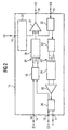
- FIG. 1 shows a first exemplary embodiment of an integrated driver module which at its output 4 provides a drive signal V out for an IGBT for controlling brushless DC and AC motors.
- the driver module present in the form of an integrated circuit 1 has connections 2, 3, 4 and 5.
- the terminal 2 is an input terminal to which an input signal V in provided at an input E is supplied, which is a signal generated in a microcontroller and is to be converted into a signal V out suitable for IGBT driving by means of the driver module.
- the terminal 3 is an input terminal for a supply voltage V cc derived from a power source.
- the terminal 4 is an output terminal for the already mentioned above drive signal V out .
- the terminal 5 is a terminal for a reference voltage V ee , preferably a ground terminal.
- the input signal V in generated by the microcontroller is first supplied to a transmitter logic 6 within the integrated circuit 1. This has the task of converting said input signal V in into a current signal which is particularly suitable for magneto-sensitive transmission. For this purpose, a signal inversion can be carried out in the transmitter logic 6, for example.
- a transformer Ü is connected, which to a magneto-sensitive transmission of the output signal the transmitter logic is provided.
- This magnetosensitive Transmission is carried out to potential isolation between the microcontroller side and the motor side of the Reach circuit. The necessity of this potential separation it follows that the microcontroller side and the motor side to different reference potentials are related.
- the transformer Ü has on the input side a conductor loop on which the present in digital form output signal the transmitter logic 6 is performed. Through this digital Signal will enter the surrounding area of the conductor loop generates a magnetic field that changes as a function of the digital signal, that indicated in the figure 1 by the dashed lines is.
- This changing magnetic field is from a Detected magnetic field detector or magneto-sensitive receiver 7, which passes through an insulator from the conductor loop is separated, but in the range of said magnetic field located.
- the magnetic field detector of the device for potential separation can be realized in the form of a Hall element. Farther It may also be in the said magnetic field detector an AMR sensor (anisotropic magnetic resistance), the change to a changing magnetic field with a resistance change responding. Such AMR sensors have a permalloy layer.
- GMR sensors have a combination of three layers, two of which are soft magnetic and a hard magnetic.
- a further improvement in the sensitivity of the magnetic field detector is thereby possible that this realized as a TMR sensor is (tunneling magnetic resistance).
- this is the hard magnetic layer through an insulating layer replaced.
- the detected by the magneto-sensitive receiver 7 signal is supplied as a galvanically separated from the input side digital signal to a control block 8. This is further connected to the terminal 3 for the supply voltage V cc and the terminal 5 for the reference voltage V ee .
- the control block 8 On the output side, the control block 8 provides a drive signal for the gate of an IGBT 9.
- a control block 8 also a magneto-sensitive transformer for potential separation between implemented on the microcontroller side and the motor side. This simplifies the circuitry, allows a less expensive production of IGBT drive circuits, allows faster switching times and simplified integration of further diagnostic, monitoring and logic components.
- FIG. 2 shows a second exemplary embodiment of a integrated driver module, which at its output 16 a drive signal S2 for the base of a not shown, arranged outside of the integrated circuit 11 IGBTs provides. This external IGBT controls one connected motor.
- the driver module present in the form of an integrated circuit 11 has connections 12, 13, 14, 15, 16, 17.
- the terminal 12 is an input terminal to which an input signal V in provided at an input E1 is supplied, which is a signal generated in a microcontroller and is to be converted into a drive signal for an IGBT by means of the driver chip.
- the terminal 13 is an input terminal for a generated by the microcontroller reset signal, which is available at the input E2.
- the terminal 14 is an input terminal for a signal of a motor-side voltage monitoring, which is supplied to the device shown via the input E3.
- the integrated circuit 11 is supplied with an input signal derived from the collector of the external IGBT, which is present at the input E4.
- the terminal 16 is an output terminal of the integrated circuit 11 at which the above-mentioned drive signal S2 for the external IGBT is output.
- the terminal 17 is an output terminal for an error signal, which is supplied from there from the microcontroller.
- the input signal V in generated by the microcontroller is first supplied to a transmitter logic 18 within the integrated circuit 11.
- This has the task to convert said input signal V in into a current signal, which is particularly well suited for magneto-sensitive transmission.
- a signal inversion can take place in the transmitter logic.
- a transformer Ü1 is connected, which leads to a magneto-sensitive transmission of the output signal the transmitter logic is provided.
- This magnetosensitive Transmission is carried out to potential isolation between the microcontroller side and the motor side of the Reach circuit. The necessity of this potential separation it follows that the microcontroller side and the motor side to different reference potentials are related.
- the transmitter Ü1 is designed as well as the above in connection with the figure 1 described transformer Ü.
- the signal detected by the magneto-sensitive receiver 19 is called as digitally isolated from the input side digital Signal is supplied to an input of a driver amplifier 21.
- Another input of this driver amplifier 21 an output signal of the circuit block 20 is supplied, which monitors the motor-side voltage and, if necessary ensures an immediate shutdown of the engine.
- the error detector 22 monitors the said input signal and ensures, for example, overcurrent for a gentle shutdown of the engine.
- the drive signal S2 provided for the external IGBT and at this via the output terminal 16 of the integrated circuit 11 forwarded.
- the error detector 22 is the output side continues with a Transmitter logic 23 connected. This has the task that the presence an error indicating output signal of the error detector 22 to convert into a current signal, which is particularly good for magneto-sensitive transmission.
- a transformer Ü2 is connected, which leads to a magneto-sensitive transmission of the output signal the transmitter logic 23 is provided.
- This magnetosensitive Transmission is carried out to potential isolation between the engine side, on which the at the entrance 15th applied signal is generated, and the microcontroller side, on which the signal provided at the output 17 available is to be reached.
- the transformer Ü2 is designed as well as the above in connection with the figure 1 described transformer Ü.
- the detected by the magneto-sensitive receiver 24 signal is signal galvanically separated from the motor side an amplifier 25 amplified and an error signal buffer 26 and the output 17 of the integrated Circuit 11 is supplied to the external microcontroller.
- the present at the input 13 of the integrated circuit Signal is a reset signal and to the microcontroller controlled Reset the error signal latch 26 provided.
- Another output of the error signal buffer is connected to an input of the transmitter logic 18 to access this Way in the presence of a fault in addition to the drive signal of the IGBT and thereby a restart to prevent the engine.
- Using integrated circuits according to the invention can both DC and AC motors be controlled.
Description
Claims (17)
- Integrierter Schaltkreis zur Erzeugung eines Ansteuersignals für einen IGBT mit einem Eingangsanschluß für ein mittels eines Mikrocontrollers erzeugtes Steuersignal und einem vom Eingangsanschluß zu einer Steuersignalverarbeitungseinheit geführten Steuersignalpfad, dadurch gekenzeichnet, daß der integrierte Schaltkreis (1, 11) im Steuersignalpfad eine erste magnetosensitive Vorrichtung (Ü, Ü1) zur Potentialtrennung, einen Eingangsanschluss (15) für ein vom Kollektor des IGBT abgeleitetes Signal und eine zweite magnetosensitive Vorrichtung (Ü2) zur Übertragung des vom Kollektor des IGBT abgeleiteten Signals aufweist.
- Integrierter Schaltkreis nach Anspruch 1, dadurch gekennzeichnet, daß er zwischen dem Eingangsanschluß (2, 12) und der ersten magnetosensitiven Vorrichtung (Ü, Ü1) zur Potentialtrennung eine Senderlogik (6, 18) aufweist.
- Integrierter Schaltkreis nach Anspruch 1 oder 2, dadurch gekennzeichnet, daß die erste magnetosensitive Vorrichtung (Ü, Ü1) eingangsseitig eine Leiterschleife und ausgangsseitig ein Magnetfelddetektorelement (7, 19) aufweist.
- Integrierter Schaltkreis nach Anspruch 3, dadurch gekennzeichnet, daß das Magnetfelddetektorelement ein Hallelement ist.
- Integrierter Schaltkreis nach Anspruch 3, dadurch gekennzeichnet, daß das Magnetfelddetektorelement ein anisotropes, magnetoresistives Bauelement (AMR) ist.
- Integrierter Schaltkreis nach Anspruch 3, dadurch gekennzeichnet, daß das Magnetfelddetektorelement ein giant magnetoresistives Bauelement (GMR) ist.
- Integrierter Schaltkreis nach Anspruch 3, dadurch gekennzeichnet, daß das Magnetfelddetektorelement ein tunnel-magnetosensitives Bauelement (TMR) ist.
- Integrierter Schaltkreis nach einem der Ansprüche 1-7, dadurch gekennzeichnet, daß er einen Ausgangsanschluß (16) für ein Ansteuersignal (S2) für einen externen IGBT aufweist.
- Integrierter Schaltkreis nach Anspruch 8, dadurch gekennzeichnet, daß er einen Treiberverstärker (21) aufweist, der das Ansteuersignal dem IGBT zur Verfügung stellt.
- Integrierter Schaltkreis nach einem der vorhergehenden Ansprüche, dadurch gekennzeichnet, daß er einen integrierten Fehlerdetektor (20, 22) aufweist.
- Integrierter Schaltkreis nach Anspruch 10, dadurch gekennzeichnet, daß der Fehlerdetektor zur Detektion mikrocontrollerseitiger Fehler vorgesehen ist.
- Integrierter Schaltkreis nach Anspruch 10 oder 11, dadurch gekennzeichnet, daß der Fehlerdetektor (20, 22) zur Detektion motorseitiger Fehler vorgesehen ist.
- Integrierter Schaltkreis nach Anspruch 12, dadurch gekennzeichnet, daß der Fehlerdetektor (22) ausgangsseitig mit der zweiten magnetosensitiven Vorrichtung (Ü2) zur Potentialtrennung verbunden ist, die ausgangsseitig mit einem Ausgangsanschluß (17) des integrierten Schaltkreises verbunden ist.
- Integrierter Schaltkreis nach Anspruch 13, dadurch gekennzeichnet, daß die zweite magnetosensitive Vorrichtung (Ü2) zur Potentialtrennung ausgangsseitig über einen Fehlersignal-Zwischenspeicher (26) mit dem Ausgangsanschluß (17) verbunden ist.
- Integrierter Schaltkreis nach Anspruch 14, dadurch gekennzeichnet, daß im Signalweg des Fehlersignals zwischen der zweiten magnetosensitiven Vorrichtung (Ü2) zur Potentialtrennung und dem Ausgangsanschluß (17) ein Verstärker (25) vorgesehen ist.
- Integrierter Schaltkreis nach Anspruch 14 oder 15, dadurch gekennzeichnet, daß der Fehlersignal-Zwischenspeicher (26) eingangsseitig mit einem Eingangsanschluß (13) des integrierten Schaltkreises für ein Reset-Signal verbunden ist.
- Integrierter Schaltkreis nach einem der Ansprüche 14-16, dadurch gekennzeichnet, daß der Fehlersignal-Zwischenspeicher (26) ausgangsseitig mit einem Eingang der im Steuersignalpfad vorgesehenen Senderlogik (18) verbunden ist.
Applications Claiming Priority (2)
| Application Number | Priority Date | Filing Date | Title |
|---|---|---|---|
| DE19922128 | 1999-05-12 | ||
| DE19922128A DE19922128C1 (de) | 1999-05-12 | 1999-05-12 | Integrierter Schaltkreis zur Erzeugung eines Ansteuersignals für einen Isolated Gate Bipolar Transistor (IGBT) |
Publications (3)
| Publication Number | Publication Date |
|---|---|
| EP1052773A2 EP1052773A2 (de) | 2000-11-15 |
| EP1052773A3 EP1052773A3 (de) | 2004-06-30 |
| EP1052773B1 true EP1052773B1 (de) | 2005-12-21 |
Family
ID=7907989
Family Applications (1)
| Application Number | Title | Priority Date | Filing Date |
|---|---|---|---|
| EP00109444A Expired - Lifetime EP1052773B1 (de) | 1999-05-12 | 2000-05-03 | Integrierter Schaltkreis zur Erzeugung eines Ansteuersignals für einen Bipolartransistor mit isoliertem Gate (IGBT) |
Country Status (4)
| Country | Link |
|---|---|
| EP (1) | EP1052773B1 (de) |
| AT (1) | ATE313875T1 (de) |
| DE (2) | DE19922128C1 (de) |
| ES (1) | ES2254069T3 (de) |
Families Citing this family (12)
| Publication number | Priority date | Publication date | Assignee | Title |
|---|---|---|---|---|
| US20030042571A1 (en) | 1997-10-23 | 2003-03-06 | Baoxing Chen | Chip-scale coils and isolators based thereon |
| US6873065B2 (en) | 1997-10-23 | 2005-03-29 | Analog Devices, Inc. | Non-optical signal isolator |
| US6262600B1 (en) | 2000-02-14 | 2001-07-17 | Analog Devices, Inc. | Isolator for transmitting logic signals across an isolation barrier |
| DE10243197B4 (de) | 2002-09-18 | 2011-05-05 | Infineon Technologies Ag | Digitales Signalübertragungsverfahren |
| EP1618712A2 (de) | 2003-04-30 | 2006-01-25 | Analog Devices, Inc. | Signalisolatoren mit mikrotransformatoren |
| US7719305B2 (en) | 2006-07-06 | 2010-05-18 | Analog Devices, Inc. | Signal isolator using micro-transformers |
| CN102263544B (zh) * | 2011-07-15 | 2013-01-02 | 武汉理工大学 | 一种带上电保护的igbt驱动电路 |
| US9293997B2 (en) | 2013-03-14 | 2016-03-22 | Analog Devices Global | Isolated error amplifier for isolated power supplies |
| US9660848B2 (en) | 2014-09-15 | 2017-05-23 | Analog Devices Global | Methods and structures to generate on/off keyed carrier signals for signal isolators |
| US10536309B2 (en) | 2014-09-15 | 2020-01-14 | Analog Devices, Inc. | Demodulation of on-off-key modulated signals in signal isolator systems |
| US10270630B2 (en) | 2014-09-15 | 2019-04-23 | Analog Devices, Inc. | Demodulation of on-off-key modulated signals in signal isolator systems |
| US9998301B2 (en) | 2014-11-03 | 2018-06-12 | Analog Devices, Inc. | Signal isolator system with protection for common mode transients |
Family Cites Families (10)
| Publication number | Priority date | Publication date | Assignee | Title |
|---|---|---|---|---|
| DE1562171B2 (de) * | 1968-03-18 | 1971-01-21 | Gehap Gesellschaft fur Handel und Patentverwertung moH & Co KG, 7595 Sas bachwalden, Erf Antrag auf Nichtnennung | Schaltungsanordnung fur ein kontakt loses Relais |
| US3631451A (en) * | 1969-12-12 | 1971-12-28 | Gehap Ges Fur Handel Und Paten | Apparatus for the contactless release of signals in clocks |
| DE2002693A1 (de) * | 1970-01-22 | 1971-07-29 | Elmatic Electronique & Automat | Relais |
| GB1397610A (en) * | 1971-07-23 | 1975-06-11 | Gehap Gmbh & Co Kg | Contactless relay |
| CH684140A5 (fr) * | 1991-01-10 | 1994-07-15 | Lem Liaisons Electron Mec | Dispositif de commande d'un transistor de puissance. |
| DE4205241C2 (de) * | 1992-02-21 | 1997-12-18 | Itt Ind Gmbh Deutsche | Potentialfreie Datenübertragungseinrichtung |
| DE4316694C1 (de) * | 1993-05-14 | 1994-10-06 | Licentia Gmbh | Hilfsstromversorgung mit integrierter Statusmeldung für Leistungshalbleiteransteuerung mit Optokopplern |
| JP2881755B2 (ja) * | 1994-04-27 | 1999-04-12 | シャープ株式会社 | パワー素子駆動回路 |
| DE19718420A1 (de) * | 1997-04-30 | 1998-11-12 | Siemens Ag | Integrierte Datenübertragungsschaltung mit Potentialtrennung zwischen Ein- und Ausgangsschaltkreis |
| AU8902598A (en) * | 1997-08-12 | 1999-03-01 | Itron Inc. | Method and apparatus for use of magnetic flux in electronic and signal processi ng systems |
-
1999
- 1999-05-12 DE DE19922128A patent/DE19922128C1/de not_active Expired - Fee Related
-
2000
- 2000-05-03 EP EP00109444A patent/EP1052773B1/de not_active Expired - Lifetime
- 2000-05-03 ES ES00109444T patent/ES2254069T3/es not_active Expired - Lifetime
- 2000-05-03 AT AT00109444T patent/ATE313875T1/de not_active IP Right Cessation
- 2000-05-03 DE DE50011887T patent/DE50011887D1/de not_active Expired - Lifetime
Also Published As
| Publication number | Publication date |
|---|---|
| DE50011887D1 (de) | 2006-01-26 |
| EP1052773A3 (de) | 2004-06-30 |
| ATE313875T1 (de) | 2006-01-15 |
| ES2254069T3 (es) | 2006-06-16 |
| DE19922128C1 (de) | 2001-01-25 |
| EP1052773A2 (de) | 2000-11-15 |
Similar Documents
| Publication | Publication Date | Title |
|---|---|---|
| EP1052773B1 (de) | Integrierter Schaltkreis zur Erzeugung eines Ansteuersignals für einen Bipolartransistor mit isoliertem Gate (IGBT) | |
| DE102014213541B4 (de) | Halbleitervorrichtung | |
| DE102011003279B4 (de) | System und Verfahren zum Testen einer Schaltung | |
| DE102006008512B4 (de) | Leistungshalbleitervorrichtung, welche mit parallel zueinander geschalteten Leistungssteuerungs-Halbleitermodulen versehen ist | |
| DE4334078A1 (de) | Steuersystem für ein elektrisches Auto | |
| DE19629934B4 (de) | Sensorsystem | |
| DE10125910A1 (de) | Verfahren und Schaltung zur Erkennung von Motor-Isolationsfehlern | |
| DE112009000503T5 (de) | Linearer Sensor mit zwei Anschlüssen | |
| DE102010049117A1 (de) | Gate-Ansteuerschaltung | |
| DE102019103030B4 (de) | Transistorvorrichtungen sowie Verfahren zur Herstellung und zum Betreiben von Transistorvorrichtungen | |
| DE102016218530A1 (de) | Weggeber zum berührungslosen Messen einer relativen Position, Herstellungsverfahren für eine Magnetfeldsensoranordnung und Magnetfeldsensor | |
| EP1339578A1 (de) | Aktiver magnetsensor für elektronische bremssysteme | |
| DE112015007039T5 (de) | Treiberschaltung für eine halbleiteranordnung und inverteranordnung | |
| DE19718420A1 (de) | Integrierte Datenübertragungsschaltung mit Potentialtrennung zwischen Ein- und Ausgangsschaltkreis | |
| DE2732626A1 (de) | Verbindungsvorrichtung zur uebertragung logischer signale | |
| DE102007006219B4 (de) | Stromsensoranordnung | |
| DE102009046691B4 (de) | Sensorvorrichtung | |
| DE10159607A1 (de) | Analog/Digital-Signalwandlereinrichtung mit galvanischer Trennung in ihrem Singalübertragungsweg | |
| DE102020207355B4 (de) | Sensorvorrichtung | |
| DE19824768A1 (de) | Leistungsverstärker und Verfahren zum Ansteuern eines Leistungsverstärkers | |
| EP0934627B1 (de) | Schaltungsanordnung zum auswerten eines binären, durch stromschwellenwerte definierten signals | |
| EP3942306B1 (de) | Leistungstransistoranordnung mit strommessschaltung | |
| DE102017101387A1 (de) | Leistungsumwandlungsvorrichtung | |
| WO2011064024A1 (de) | Schaltungseinrichtung und leistungsschaltkreis mit der schaltungseinrichtung | |
| DE102021209365A1 (de) | Impulssignalvervielfacher zur Bereitstellung eines sekundären Impulssignals aus einem primären Impulssignal eines Impulssignalgebers |
Legal Events
| Date | Code | Title | Description |
|---|---|---|---|
| PUAI | Public reference made under article 153(3) epc to a published international application that has entered the european phase |
Free format text: ORIGINAL CODE: 0009012 |
|
| AK | Designated contracting states |
Kind code of ref document: A2 Designated state(s): AT BE CH CY DE DK ES FI FR GB GR IE IT LI LU MC NL PT SE |
|
| AX | Request for extension of the european patent |
Free format text: AL;LT;LV;MK;RO;SI |
|
| PUAL | Search report despatched |
Free format text: ORIGINAL CODE: 0009013 |
|
| AK | Designated contracting states |
Kind code of ref document: A3 Designated state(s): AT BE CH CY DE DK ES FI FR GB GR IE IT LI LU MC NL PT SE |
|
| AX | Request for extension of the european patent |
Extension state: AL LT LV MK RO SI |
|
| 17P | Request for examination filed |
Effective date: 20040719 |
|
| 17Q | First examination report despatched |
Effective date: 20040823 |
|
| AKX | Designation fees paid |
Designated state(s): AT CH DE ES FR GB LI |
|
| GRAP | Despatch of communication of intention to grant a patent |
Free format text: ORIGINAL CODE: EPIDOSNIGR1 |
|
| GRAS | Grant fee paid |
Free format text: ORIGINAL CODE: EPIDOSNIGR3 |
|
| GRAA | (expected) grant |
Free format text: ORIGINAL CODE: 0009210 |
|
| AK | Designated contracting states |
Kind code of ref document: B1 Designated state(s): AT CH DE ES FR GB LI |
|
| REG | Reference to a national code |
Ref country code: GB Ref legal event code: FG4D Free format text: NOT ENGLISH |
|
| REG | Reference to a national code |
Ref country code: CH Ref legal event code: NV Representative=s name: SIEMENS SCHWEIZ AG Ref country code: CH Ref legal event code: EP |
|
| GBT | Gb: translation of ep patent filed (gb section 77(6)(a)/1977) |
Effective date: 20051221 |
|
| REF | Corresponds to: |
Ref document number: 50011887 Country of ref document: DE Date of ref document: 20060126 Kind code of ref document: P |
|
| REG | Reference to a national code |
Ref country code: ES Ref legal event code: FG2A Ref document number: 2254069 Country of ref document: ES Kind code of ref document: T3 |
|
| ET | Fr: translation filed | ||
| PLBE | No opposition filed within time limit |
Free format text: ORIGINAL CODE: 0009261 |
|
| STAA | Information on the status of an ep patent application or granted ep patent |
Free format text: STATUS: NO OPPOSITION FILED WITHIN TIME LIMIT |
|
| 26N | No opposition filed |
Effective date: 20060922 |
|
| PGFP | Annual fee paid to national office [announced via postgrant information from national office to epo] |
Ref country code: ES Payment date: 20080611 Year of fee payment: 9 |
|
| PGFP | Annual fee paid to national office [announced via postgrant information from national office to epo] |
Ref country code: AT Payment date: 20080416 Year of fee payment: 9 |
|
| PGFP | Annual fee paid to national office [announced via postgrant information from national office to epo] |
Ref country code: CH Payment date: 20080807 Year of fee payment: 9 |
|
| REG | Reference to a national code |
Ref country code: CH Ref legal event code: PCAR Free format text: SIEMENS SCHWEIZ AG;INTELLECTUAL PROPERTY FREILAGERSTRASSE 40;8047 ZUERICH (CH) |
|
| REG | Reference to a national code |
Ref country code: CH Ref legal event code: PL |
|
| PG25 | Lapsed in a contracting state [announced via postgrant information from national office to epo] |
Ref country code: LI Free format text: LAPSE BECAUSE OF NON-PAYMENT OF DUE FEES Effective date: 20090531 Ref country code: AT Free format text: LAPSE BECAUSE OF NON-PAYMENT OF DUE FEES Effective date: 20090503 Ref country code: CH Free format text: LAPSE BECAUSE OF NON-PAYMENT OF DUE FEES Effective date: 20090531 |
|
| REG | Reference to a national code |
Ref country code: ES Ref legal event code: FD2A Effective date: 20090504 |
|
| PG25 | Lapsed in a contracting state [announced via postgrant information from national office to epo] |
Ref country code: ES Free format text: LAPSE BECAUSE OF NON-PAYMENT OF DUE FEES Effective date: 20090504 |
|
| PGFP | Annual fee paid to national office [announced via postgrant information from national office to epo] |
Ref country code: GB Payment date: 20110512 Year of fee payment: 12 |
|
| GBPC | Gb: european patent ceased through non-payment of renewal fee |
Effective date: 20120503 |
|
| PG25 | Lapsed in a contracting state [announced via postgrant information from national office to epo] |
Ref country code: GB Free format text: LAPSE BECAUSE OF NON-PAYMENT OF DUE FEES Effective date: 20120503 |
|
| PGFP | Annual fee paid to national office [announced via postgrant information from national office to epo] |
Ref country code: DE Payment date: 20150720 Year of fee payment: 16 |
|
| REG | Reference to a national code |
Ref country code: FR Ref legal event code: PLFP Year of fee payment: 17 |
|
| PGFP | Annual fee paid to national office [announced via postgrant information from national office to epo] |
Ref country code: FR Payment date: 20160512 Year of fee payment: 17 |
|
| REG | Reference to a national code |
Ref country code: DE Ref legal event code: R119 Ref document number: 50011887 Country of ref document: DE |
|
| PG25 | Lapsed in a contracting state [announced via postgrant information from national office to epo] |
Ref country code: DE Free format text: LAPSE BECAUSE OF NON-PAYMENT OF DUE FEES Effective date: 20161201 |
|
| REG | Reference to a national code |
Ref country code: FR Ref legal event code: ST Effective date: 20180131 |
|
| PG25 | Lapsed in a contracting state [announced via postgrant information from national office to epo] |
Ref country code: FR Free format text: LAPSE BECAUSE OF NON-PAYMENT OF DUE FEES Effective date: 20170531 |