EP1052724B1 - Structure inductive grillagée - Google Patents
Structure inductive grillagée Download PDFInfo
- Publication number
- EP1052724B1 EP1052724B1 EP20000401264 EP00401264A EP1052724B1 EP 1052724 B1 EP1052724 B1 EP 1052724B1 EP 20000401264 EP20000401264 EP 20000401264 EP 00401264 A EP00401264 A EP 00401264A EP 1052724 B1 EP1052724 B1 EP 1052724B1
- Authority
- EP
- European Patent Office
- Prior art keywords
- elementary
- grids
- structure according
- diffraction
- grid
- Prior art date
- Legal status (The legal status is an assumption and is not a legal conclusion. Google has not performed a legal analysis and makes no representation as to the accuracy of the status listed.)
- Expired - Lifetime
Links
- 230000001939 inductive effect Effects 0.000 title claims description 52
- 230000003287 optical effect Effects 0.000 claims description 96
- 230000003595 spectral effect Effects 0.000 claims description 37
- 230000000737 periodic effect Effects 0.000 claims description 20
- 239000011295 pitch Substances 0.000 claims description 14
- 230000002093 peripheral effect Effects 0.000 claims description 4
- 230000001154 acute effect Effects 0.000 claims description 2
- 230000005540 biological transmission Effects 0.000 description 27
- 238000011084 recovery Methods 0.000 description 13
- 238000012216 screening Methods 0.000 description 8
- 239000000463 material Substances 0.000 description 6
- 239000004065 semiconductor Substances 0.000 description 6
- 230000001788 irregular Effects 0.000 description 5
- 239000011800 void material Substances 0.000 description 5
- 230000007423 decrease Effects 0.000 description 4
- 230000008878 coupling Effects 0.000 description 3
- 238000010168 coupling process Methods 0.000 description 3
- 238000005859 coupling reaction Methods 0.000 description 3
- 230000000694 effects Effects 0.000 description 3
- 230000016571 aggressive behavior Effects 0.000 description 2
- 238000004519 manufacturing process Methods 0.000 description 2
- 239000012811 non-conductive material Substances 0.000 description 2
- 230000010287 polarization Effects 0.000 description 2
- 101100294399 Schizosaccharomyces pombe (strain 972 / ATCC 24843) not1 gene Proteins 0.000 description 1
- 230000002238 attenuated effect Effects 0.000 description 1
- 230000008033 biological extinction Effects 0.000 description 1
- 230000003247 decreasing effect Effects 0.000 description 1
- 230000000593 degrading effect Effects 0.000 description 1
- 230000001419 dependent effect Effects 0.000 description 1
- 230000002542 deteriorative effect Effects 0.000 description 1
- 239000002184 metal Substances 0.000 description 1
- 238000001228 spectrum Methods 0.000 description 1
Images

Classifications
-
- H—ELECTRICITY
- H01—ELECTRIC ELEMENTS
- H01Q—ANTENNAS, i.e. RADIO AERIALS
- H01Q15/00—Devices for reflection, refraction, diffraction or polarisation of waves radiated from an antenna, e.g. quasi-optical devices
- H01Q15/0006—Devices acting selectively as reflecting surface, as diffracting or as refracting device, e.g. frequency filtering or angular spatial filtering devices
- H01Q15/0013—Devices acting selectively as reflecting surface, as diffracting or as refracting device, e.g. frequency filtering or angular spatial filtering devices said selective devices working as frequency-selective reflecting surfaces, e.g. FSS, dichroic plates, surfaces being partly transmissive and reflective
- H01Q15/0026—Devices acting selectively as reflecting surface, as diffracting or as refracting device, e.g. frequency filtering or angular spatial filtering devices said selective devices working as frequency-selective reflecting surfaces, e.g. FSS, dichroic plates, surfaces being partly transmissive and reflective said selective devices having a stacked geometry or having multiple layers
Definitions
- the invention relates to the field of inductive structures screened.
- Inductive mesh structures can be used as microwave short-circuit for the protection of optical equipment or optronics against electromagnetic aggression so that the equipment behaves roughly like a Faraday cage.
- the electromagnetic aggression can be of the type radio, radar, weapon microwave, strong field, electromagnetic pulse, lightning ... optronic equipment can encompass all types of equipment having an optical opening closed by a window guaranteeing the mechanical closure of the material.
- the porthole must then also realize to a certain extent the electrical closure of the material by presenting a low impedance on a given microwave spectral domain.
- the door must have the following properties, on the one hand the microwave shielding property of screening substantially in a given microwave spectral range, by example from 2 to 18 GHz, and secondly the optical transmission property to be substantially transparent in a spectral range given optical, for example from the ultraviolet to the infrared, and present a good modulation transfer function in the field optical spectral.
- a problem to solve by the portholes is that of a good compromise between microwave properties and optical properties, that is to say between the microwave shielding and the optical transmission which will be called in the following the "microwave / optical compromise". Indeed, these properties are difficult to reconcile and often, a good screening microwave can only be obtained at the expense of the transmission optically, whether at the level of optical transparency, that is to say amount of energy transmitted or at the level of the transfer function of modulation, ie the quality of the energy transmitted, and vice versa. In Depending on the type of application envisaged, different solutions are possible.
- a porthole comprising a thick layer of semiconductor.
- Selective doping in the form of Grid of the semiconductor layer allows to obtain the property of screening. Due to the low electrical conductivity of semiconductors, good microwave shielding can only be achieved with a thick semiconductor layer, which has the effect of to degrade the optical transparency and therefore the optical transmission. In the case of severe constraints, the microwave / optical compromise achieved will be insufficient. Moreover, it is difficult to find a semiconductor material having good optical transparency in the field optical spectral of the visible.
- a porthole comprising a thin layer of material with high electrical conductivity.
- the material of the thin layer must have a high electrical conductivity and therefore a high extinction coefficient even at optical wavelengths, thus degrading the optical transparency and therefore the optical transmission.
- the microwave / optical compromise realized will be insufficient.
- a structure is provided Inductive grid bicriodic grille type square pattern for example.
- the square character ensures the symmetry of the polarity as well as a relative simplicity of the grid.
- the grid material is electrically conductive, it is for example a metal or a semiconductor. Either at the time or the not network and 2d the wire width of the grid.
- the 2d / a ratio influences important way microwave shielding. A high 2d / a ratio is translated by good microwave shielding and vice versa. But a report 2d / a high implies a recovery rate, ie a ratio between conductive surface and total area for the grid, which is also high.
- This high recovery rate is a source of diffraction phenomenon which degrades the quality of the optical transmission by deteriorating the function modulation transfer.
- the Microwave / optical compromise achieved will be insufficient. It remains possible at constant ratio 2d / a, to decrease the step a of the grid and consequently the 2d wire width of the grid. Wavelengths in the spectral domain microwave being greater than the wavelengths in the field spectral range, the decrease of the step at constant 2d / a ratio affects more microwave wavelengths as optical wavelengths. While the cutoff frequency in the spectral range microwave frequency increases and that the microwave shielding improves, the diffraction phenomenon is little changed and the optical transmission is therefore degrades little. Nevertheless, in the case of severe constraints, the compromise microwave / optical realized will still be insufficient.
- the invention is based on a very clear improvement of the compromise microwave / optical.
- the invention uses an inductive structure mesh having in particular a good microwave shielding as well a more uniform spatial distribution of optical diffraction energy, that is, diffraction energy in the optical spectral range.
- the quality of the optical transmission of the inductive mesh structure and the entire optical window in which the grid may be included, in is then significantly improved, since a more uniform spatial distribution optical diffraction energy improves the transfer function of modulation.
- the invention also has the advantage of proposing a solution bandwidth for the optical spectral range, because the grid-like character of the inductive structure allows the optical transmission in the field optical spectral to be somewhat dependent on the optical wavelength.
- an inductive mesh structure having elementary meshes whose sides are in wire electrically conductive, the average recovery rate of the meshes elementary being on the one hand sufficiently high for the structure substantially scoring in a given microwave spectral domain and on the other hand weak enough for the structure to be substantially transparent in a given optical spectral range, characterized in that the sides of the stitches are oriented sufficiently irregular to spatially distribute more evenly in the case of a single periodic grid, the diffraction energy in the optical spectral domain.
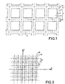
- Figure 1 makes it possible to specify some general definitions concerning the elementary meshes of any grid.
- the example shown relates to a grid with square patterns composed of several elementary meshes m as the grids according to the third prior art.
- the elemental meshes m are represented in dashed lines.
- Each elemental mesh has a surface sv of vacuum or electrically non-conductive material surrounded by electrically conductive wire sides constituting the surface sf of wire.
- 2d represents the wire width and has the pitch of the mesh.
- the rate of vacuum or electrically non-conductive material is sv / a 2 and the recovery rate is (a 2 -sv) / a 2 , where sv is here (a-2d) 2 .
- the elementary mesh surface is 2 .
- the sides of the elementary meshes of the inductive mesh structure are oriented more irregular way than are the sides of the elemental meshes a periodic single grid, such as a grid with square patterns or circulars.
- a periodic single grid such as a grid with square patterns or circulars.
- the microwave spectral domain it is This is for the inductive mesh structure to keep as much as possible the periodic character of a periodic single grid.
- the optical spectral domain this is for the inductive mesh structure, all maintaining the good optical transparency of a single periodic grid low recovery rate, to minimize the character periodical of a single periodic grid.
- Inductive mesh structure according to the invention takes advantage of the fact that the wavelengths of the domain spectral spectra are lower and often significantly lower than wavelengths of the microwave spectral domain.
- This spatial distribution more uniform optical diffraction energy allows, for an energy globally diffracted equivalent, relocating this energy by spatial distribution, thereby decreasing the intensity of the diffraction peaks of the diffraction pattern of the inductive mesh structure, to improve considerably the modulation transfer function and therefore the quality of the optical transmission.
- the first type uses several mesh inductive structures, for example grids, each of which may have a significant periodic the layout and layout diminish the periodic nature of the set constituted by the different structures. This solution is relatively simple to achieve but its effectiveness is not totally optimized.
- the first type corresponds to the first two modes of production.
- the second type uses a single grid structure whose aperiodic character is important. This solution is more complex to achieve but is likely to give even better results.
- the second type corresponds to the third embodiment.
- the solutions of the two types of devices can of course be combined for one even greater efficiency at the cost of a complexity of realization which increases.
- the first type of device uses an inductive structure mesh having several elementary grids diffracting each according to a pattern of diffraction peaks, the figures of diffraction peaks being substantially spatially shifted between them.
- the optimum is reached when the diffraction peaks from one figure to another are spatially distinct, that is to say do not overlap at all; however, a slight recovery can result in a satisfactory solution, in particular depending on the type and severity of the constraints imposed by the application considered.
- the more the diffraction patterns are spatially shifted the more the diffraction energy in the optical spectral domain is spatially evenly distributed, and better is the quality of the transmission optical.
- the intensity of the corresponding diffraction peaks remains preferably substantially constant from one figure to another. So the energy of diffraction in the optical spectral range is distributed substantially identical between the different diffraction figures corresponding to the different elementary grids. More peak intensity of diffraction from one figure to another is constant, plus diffraction energy in the optical spectral domain is uniformly spatially distributed.
- the structure functionally comprises several grids elementals virtually each having a diffraction pattern, but these elementary grids all preferentially occupy the same surface and structurally preferably form a single grid. In the case of planar elementary grids, all the elementary grids will then be in the same plane and assembled to each other so as to no longer structurally form a single resulting grid. If the different grids Each elementary element has a very marked periodic character, for example square patterns regularly spaced, the layout of these elementary grids will be such that the periodic character of the grid resultant will be much less marked, its reasons being then for example polygons more or less regular.
- the advantage of such a structure mesh is to have an optical transmission comparable to that of one elementary grids while having microwave shielding significantly improved.
- the elementary grids are substantially parallel to each other but where they do not belong to the same surface, the elementary grids must be sufficiently close from each other, that is to say that the distance between the grids elementary needs to remain low enough for the irregular character of the orientation of the sides of the elementary meshes translates into a more uniform spatial distribution of energy optical diffraction.
- a structure consisting of two elementary orientation grids different, square patterns, and separated by enough space important in relation to optical wavelengths will diffract mainly in two directions as a periodic single grid.
- the grids Elementals have substantially the same recovery rate.
- the optimum being reached when the recovery rate is identical.
- Grates elementary elements advantageously have elementary meshes of substantially square.
- the substantially square character of the stitches elementary offers a good compromise between simplicity, screening microwave, optical transmission and polarization symmetry, even if the intensity of the diffraction peaks remains higher than with grids Elementals whose patterns have a more "irregular" shape.
- FIG. 2 schematically shows a first mode particular embodiment of a mesh inductive structure according to the invention.
- the structure has several elementary grids, here two grids elementary G1 and G2.
- the G2 grid is represented in phantom while the grid G1 is represented in dashed lines.
- elementary grids belong to substantially parallel surfaces between them, advantageously flat.
- grids elementals are in the same plane and their elementary mesh sides get cross so as to form a single mesh structure.
- Each of the elementary grids has an elementary mesh surface substantially constant and the elementary mesh surfaces are substantially different between elementary grids.
- the two elementary grids G1 and G2 have elemental meshes of substantially square shape.
- Grates elementary elements all advantageously have the same orientation, that is to say that the sides of the elemental meshes of one of the grids are respectively parallel to the elementary meshes of the others elementary grids. This will be the case for all numerical examples in the first embodiment.
- the two grids elementary G1 and G2 have elementary mesh sides that are respectively parallel to the two axes X and Y perpendicular to each other.
- the pitch a1 is equal to 10 ⁇ m and the pitch a2 is equal to 13 ⁇ m.
- the wire width 2d is chosen equal to 2 .mu.m.
- the ratio between wire width and pitch, namely 2d / a1 is 0.2.
- the ratio between wire width and not worth 0.154 Let us assign the index n to the diffraction orders corresponding to the first elementary grid G1.
- the different peaks of diffraction of order n are angularly located, from the center of the spot diffraction center at angles of n ⁇ / a1.
- the orders of diffraction of order m corresponding to the second elementary grid G2 are angularly, from the center of the central diffraction spot, to angles worth m ⁇ / a2. If, as is the case, the respective steps a1 and a2 elementary grids G1 and G2 are different, the diffraction peaks, although located in the same directions X and Y, however, are for the most of them, distinct from each other.
- these overlaps should not be produce that for high diffraction orders so that the resulting energy of the sum of the two corresponding diffraction peaks is less than the optical diffraction energy of the first peaks of diffraction of at least one of the elementary grids.
- the steps of different elementary grids are chosen so that any diffraction peak resulting from the total or partial superposition of several peaks of diffraction from different elementary grids has an intensity that is less than or substantially equal to the highest of all intensities of first order diffraction peaks of all grids elementary. So the diffraction peaks resulting from the coupling between diffraction orders of several elementary grids, then correspond to high diffraction orders and therefore low energy. So, these diffraction peaks resulting from the coupling between elementary grids are not not limiting, since lower in intensity at the first diffraction peaks at least one of the elementary grids.
- the steps of the different elementary grids are also preferentially chosen so that any diffraction peak resulting from the total or partial superposition of several peaks of diffraction from different elementary grids and whose intensity is greater than or substantially equal to the highest of all intensities first order diffraction peaks of all elementary grids, is located outside the field of the optical window in which the grid structure is integrated.
- the diffraction peaks resulting from the coupling between orders of diffraction of several elementary grids, corresponding then to diffraction orders located outside the field of the optronic window are not not limiting, since excluded from the image of the scene observed through the optronic window.
- Example 1 the energies of the different diffraction peaks on the one hand for each of the elementary grids G1 and G2 and on the other hand for the inductive mesh structure SIG consisting of set of two elementary roasts G1 and G2.
- the diffraction order is indicated in parentheses with the corresponding grid or structure: for example 2 (G2) means "second diffraction order for the elementary gate G2. Since the void ratio of a grid is the ratio between the void surface and the total area, the grids G1 and G2 respectively have a void ratio of 64% and 71%, whereas the inductive mesh structure, denoted SIG, has a vacuum rate of 47%.
- the energies are denoted in arbitrary relative units, with the value 1 corresponding to the energy of the central diffraction spot.
- the sixth order of diffraction for the inductive structure GIS mesh corresponds respectively to the third and fourth orders diffraction pattern for the first G1 and second G2 elementary grids.
- the energy of this sixth order of diffraction for the inductive structure SIG mesh is approximately the sum of the energy of the third and fourth order of diffraction for the first G1 and second G2 elemental grids respectively. But this remaining amount less than the energy of the second order of diffraction for the structure inductive mesh corresponding to the first order of diffraction of the first grid G1, the diffraction peak of the sixth diffraction order for the Inductive mesh structure is not limiting.
- a total decoupling between the diffraction orders of the different component elementary grids structure and thus excluding any recovery of peaks from Even partial diffraction remains difficult to achieve.
- an inductive mesh structure makes it possible, while having an optical transmission quality comparable to that of the optically most limiting elementary grid, to the inductive structure.
- grid to have a significantly improved microwave overfrequency shielding compared to the microwave shielding of the best elemental grid in the microwave spectral range.
- An optical transmission of good quality corresponds to a ratio between the energy of the first diffraction peak and the energy of the central diffraction spot which is low in the optical spectral range, here the optical domain ranging for example from the ultraviolet infrared. This report will be noted E1.0 / E0.0.
- a good microwave shielding corresponds to an attenuation on a given microwave band, here the band ranging for example from 2 to 18 GHz.
- the elementary grid G1 has a pitch a1 equal to 200 ⁇ m, a width of wire 2d equal to 1 ⁇ m and a total surface area to wire ratio of 0.005.
- the elementary grid G2 has a pitch a2 equal to 220 ⁇ m, a width of wire 2d equal to 1 ⁇ m and a surface area of wire to total surface of 0.0045.
- the ratio E1.0 / E0.0 and the attenuation T2-18GHz are respectively given in relative value and in decibel (dB), for each of the elementary grids G1 and G2 and for the inductive structure SIG constituted by these two grids elementary.
- G1 G2 GIS E1.0 / E0,0 2.5x10 -5 2.1x10 -5 2.5x10 -5 T2-18GHz -25.4 -24.5 -31.4
- the microwave gain is 6dB, which is important. The compromise thus achieved between the microwave shielding and the quality of the optical transmission is thus significantly improved.
- the position of the elementary grids relative to each other in the same plane does not have a significant influence on the quality of the optical transmission. Indeed, when the two elementary grids G1 and G2 are shifted relative to each other, the variation of the ratio between the total energy diffracted in the higher orders and the energy of the spot diffraction center is negligible, of the order of a fraction of a percent.
- Microwave shielding corresponds to an attenuation on a given microwave band, here the band ranging for example from 2 to 18 GHz. This attenuation is noted T2-18GHz, it is given in dB.
- the elementary grid G1 has a pitch a1 equal to 2 mm, a wire width 2 d equal to 2 ⁇ m and a total surface area to wire ratio of 0.001.
- the elementary grid G2 has a pitch a2 equal to 2.1mm, a wire width 2d equal to 2 ⁇ m, and a total surface area to wire ratio of 0.00095.
- An additional grid with a pitch of 1 mm and a total surface-to-surface ratio of 0.002, denoted Geqhyp for "grid equivalent to the inductive grid structure in the microwave spectral domain", is contained in the table to show the impossibility with a periodic single grid to perform a microwave / optical compromise as good as with the inductive gate mesh according to the invention.
- the corresponding numerical results are collated in the third table.
- the third table shows that for a diffraction quality similar to that of each of the elementary grids G1 and G2, the microwave shielding is improved by about 5 dB.
- the Geqhyp "equivalent grid" has a ratio between the maximum energy of a higher order diffraction peak and the energy of the diffraction center spot. the optical spectral range, which is four times higher, which represents a much lower optical transmission quality.
- a fourth table groups above the numerical results of a fourth numerical example.
- the notations of the third numerical example described above are preserved.
- Several elementary grids G1, G2, G3, G4, G5, G6 are considered, they have respective not1 values equal to 2mm, a2 being equal to 2.1mm, a3 being equal to 2.2mm, a4 being equal to 2.3mm, a5 being equal to 2.4mm, a6 worth 2.5mm.
- Several meshed inductive structures containing from two to six elementary grids are analyzed.
- the grid structures SIG (G1 to G2), GIS (G1 to G3), GIS (G1 to G4), GIS (G1 to G5), GIS (G1 to G6) respectively consist of elementary gates G1 to G2, G1 to G1. G3, G1 to G4, G1 to G5, G1 to G6.
- the fourth table contains two additional grids with respective pitch values of 0.46 mm and 2 mm, as well as surface area to wire ratios of 0.0043 and 0.001 respectively, respectively denoted Geqhyp for "grid equivalent to the inductive grid structure in the microwave spectral domain "and Geqopt for" grid equivalent to the inductive lattice structure in the optical spectral domain ".
- Eoptique E0,0 Ei, 0 / E0,0 T2-18GHz GIS G1 to G2 0.996 0,992 10 -6 -13 GIS (G1 to G3) 0,994 0.988 10 -6 -15.4 GIS (G1 to G4) 0,992 0,985 10 -6 -17.5 GIS (G1 to G5) 0.99 0.982 10 -6 -19.1 GIS (G1 to G6) 0.988 0.979 10 -6 -20.5 Geqhyp 0.991 0.983 1,9x10 -5 -20.5 Geqopt 0,998 0.996 10 -6 -8.2
- the microwave gain is worth approximately 2.4 dB, the same gain from five to six grids is only 1.4dB.
- the inductive mesh structure comprising six elementary grids achieves a very good microwave / optical compromise.
- the gain at the maximum relative intensity level of the diffraction peaks represented by the ratio Ei, 0 / E0,0 which is a key parameter reflecting the quality of the optical transmission, reaches a factor of 19.
- the gain at the level of Microwave shielding reaches 12dB, which corresponds to a factor of 16.
- optical transparency represented by the value of the overall optical transmission E0,0 very drop slightly, about 1% between the inductive mesh structure comprising six elementary grids and the "optical equivalent grid" Geqopt.
- the number of grids is not a realizing parameter really limiting, since only the wire width is technologically limiting.
- FIG. 3 schematically shows a second mode particular embodiment of a mesh inductive structure according to the invention.
- the structure has several elementary grids, here two grids elementary G1 and G2.
- the two elementary grids G1 and G2 are represented in solid lines.
- the elementary grids belong to surfaces substantially parallel to each other, advantageously flat.
- the elementary grids are in the same plane and their elementary mesh sides intersect so to form only a single grid structure.
- Each of the grids elementary has a substantially constant elementary mesh surface and elementary mesh surfaces are substantially shifted angularly between them.
- the elementary grids G1 and G2 are angularly offset by an angle ⁇ .
- the two elementary grids G1 and G2 have elementary meshes of substantially square shape.
- the elementary grids G1 and G2 have steps respective a1 and a2.
- Elementary grids all advantageously have the not even, that is to say that the sides of the elementary meshes of one of the grids are respectively of length equal to that of the sides of the meshes elements of the other elementary grids. This will be the case for fifth preferred numerical example relating to the second mode of production.
- the elementary grid G1 has elementary mesh sides which are respectively parallel to the two perpendicular x and y axes between them, while the elementary grid G2 has elementary mesh sides that are respectively parallel to the two perpendicular X and Y axes between them.
- the inductive mesh structure may have more than two grids elementary.
- the structure comprising N elementary grids, the grids elementary elements are preferably offset from each other by an angle substantially ⁇ / 2N, especially when there are three or more elementary grids.
- ⁇ / 2N substantially ⁇ / 2N
- the pics diffraction patterns correspond to the energy diffracted in the parallel directions to the sides of the grid, while secondary peaks of diffraction correspond to the energy diffracted in non-direction parallel to the sides of the grid, this energy being much lower than the often to that of the main diffraction peaks.
- Each of the elementary grids diffracts, at least mainly, according to different axes.
- the elementary grid G1 diffracts mainly in the x and y directions, while the elementary grid G2 diffracts mainly in the X and Y directions.
- the optical diffraction energy is spatially distributed more evenly than in the case of a single grid, and even more evenly than in the case of grids same orientation as in the case of Figure 2, since here not only the diffraction figures of the elementary grids the respective directions do not overlap or which they extend are distinct.
- Optical diffraction energy is spatially distributed in many directions and no longer only mainly according to two privileged directions as in the case of Figure 2.
- screening microwave appears to be best of about 6dB, which represents a very clear improvement of the microwave / optical compromise.
- the superposition of two elementary grids each screening -16dB microwave does not result in screening resulting from -32dB which would be the sum of the previous ones, because the distance between the elementary grids is weak enough (here it is even nil since the grids are in the same plane) so that the two grids Elementals interact on the waves that pass through them.
- FIG. 4 schematically shows a third mode particular embodiment of a mesh inductive structure according to the invention having at least one grid like that shown in FIG.
- FIG. 4 represents a Gap gate whose aperiodic character is important.
- the elementary meshes have substantially the same surface and the same form.
- the size elemental meshes is small enough in front of the lengths of microwave wave so that the elementary meshes appear all similar when "seen" by wavelengths microwave.
- the Gap grid has microwave properties comparable to those of a single periodic grid such as for example a grid patterned squares, and it can in the same way screen substantially in the microwave domain.
- a grid single periodic usually has peaks of intensity diffraction relative high.
- the mesh sides are oriented so that the diffraction zones of the structure are spatially distributed so substantially homogeneous.
- the diffraction energy optical is for example spatially distributed according to more than two directions and / or in non-rectilinear forms and / or in larger areas that the very localized diffraction peaks of a periodic single grid, resulting in a substantially homogeneous spatial distribution.
- the gate G does not have an acute angle between adjacent sides of elementary mesh because sharp angles between meshes elementals are at the source of local diffraction phenomena but intense. All angles between adjacent sides of elemental mesh are advantageously substantially equal to ⁇ / 2.
- Two adjacent sides of the elementary mesh mj are for example c1 and c2.
- the preferred form of the grid G shown in FIG. 4 is a grid whose elementary meshes are angular sectors of concentric rings.
- the gate G comprises a central circular zone O comprising one or more elementary meshes, here two.
- Around this central circular zone O are a set of concentric rings, here three.
- the concentric rings P, Q and R which are here the first, second and third peripheral crowns, each comprise several elementary meshes of the type of the mesh mi or the mesh mj.
- the rings have substantially constant widths and substantially equal to each other.
- the central circular zone O can be considered as the central crown in the formula below.
- the M th peripheral ring from the central ring advantageously comprises K (2M + 1) elemental meshes.
- the elementary meshes all have substantially the same surface and the same shape as the meshes mi and mj.
- the third peripheral crown will then comprise fourteen.
- the grid G preferably has roughly axial symmetry, as for example in Figure 4, for reasons of polarization symmetry.
- the grid G can have, at the scale optical wavelengths, elementary mesh sides whose irregularity of the orientation is more marked than in the case of right segments joining the inner and outer perimeters of the same crowned.
- the sides of the elementary meshes connecting the inner perimeters and outer of the same crown can then advantageously be inclined relative to the norm at the perimeters of the crowns.
- Elemental stitches may also not be straight. for example arcs between the perimeters of the crowns would allow even better to spatially distribute the optical diffraction energy in space.
- Another solution could use at least one grid constituted by a set of elliptical shapes whose major axes all have different lengths and / or different directions. So, almost none sides of the elementary meshes would be parallel to each other and the optical diffraction energy would be spatially distributed all the more uniform.
Landscapes
- Diffracting Gratings Or Hologram Optical Elements (AREA)
- Optical Modulation, Optical Deflection, Nonlinear Optics, Optical Demodulation, Optical Logic Elements (AREA)
- Optical Filters (AREA)
Description
- la figure 1 représente schématiquement une maille élémentaire d'une grille à motifs carrés selon le troisième art antérieur ;
- la figure 2 représente schématiquement un premier mode particulier de réalisation d'une structure inductive grillagée selon l'invention ;
- la figure 3 représente schématiquement un deuxième mode particulier de réalisation d'une structure inductive grillagée selon l'invention ;
- la figure 4 représente schématiquement un troisième mode particulier de réalisation d'une structure inductive grillagée selon l'invention.
| Ordre de diffraction | G1 | G2 | SIG |
| 0(G1) ; 0(G2) ; 0(SIG) | 1 | 1 | 1 |
| 1(G2) ; 1(SIG) | ≈0 | 0,029 | 0,03 |
| 1(G1) ; 2(SIG) | 0,064 | ≈0 | 0,067 |
| 2(G2) ; 3(SIG) | ≈0 | 0,025 | 0,024 |
| 2(G1) ; 4SIG) | 0,037 | ≈0 | 0,032 |
| 3(G2) ; 5(SIG) | ≈0 | 0,024 | 0,02 |
| 3(G1) ; 4(G2) ; 6(SIG) | 0,023 | 0,011 | 0,039 |
| G1 | G2 | SIG | |
| E1,0/E0,0 | 2,5x10⁻⁵ | 2,1x10⁻⁵ | 2,5x10⁻⁵ |
| T2-18GHz | -25,4 | -24,5 | -31,4 |
| G1 | G2 | SIG | Geqhyp | |
| Eoptique | 0,998 | 0,998 | 0.996 | 0,996 |
| E0,0 | 0,996 | 0,996 | 0,992 | 0,992 |
| Ei,0/E0,0 | 10-6 | 9,1x10⁻⁷ | 10-6 | 4x10⁻⁶ |
| T2-18GHz | -8,2 | -7,8 | -13 | -13 |
| Eoptique | E0,0 | Ei,0/E0,0 | T2-18GHz | |
| SIG(G1 à G2) | 0,996 | 0,992 | 10-6 | -13 |
| SIG(G1 à G3) | 0,994 | 0,988 | 10-6 | -15,4 |
| SIG(G1 à G4) | 0,992 | 0,985 | 10-6 | -17,5 |
| SIG(G1 à G5) | 0,99 | 0,982 | 10-6 | -19,1 |
| SIG(G1 à G6) | 0,988 | 0,979 | 10-6 | -20,5 |
| Geqhyp | 0,991 | 0,983 | 1,9x10⁻⁵ | -20,5 |
| Geqopt | 0,998 | 0,996 | 10-6 | -8,2 |
| G1 | G2 | SIG | |
| E1,0/E0,0 | ≈10-5 | ≈10-5 | ≈10-5 |
| T2-18GHz | -16 | -16 | -22,1 |
Claims (22)
- Structure inductive grillagée (SIG) comportant des mailles (mi, mj) élémentaires dont les côtés (c1, c2) sont en fil électriquement conducteur, le taux de recouvrement moyen des mailles élémentaires étant d'une part suffisamment élevé pour que la structure écrante substantiellement dans un domaine spectral hyperfréquence donné et d'autre part suffisamment faible pour que la structure soit substantiellement transparente dans un domaine spectral optique donné, caractérisé en ce que les côtés des mailles (mi, mj) sont orientés de manière suffisamment irrégulière pour répartir spatialement de manière plus uniforme que dans le cas d'une grille unique périodique, l'énergie de diffraction dans le domaine spectral optique.
- Structure selon la revendication 1, caractérisé en ce que la structure (SIG) comporte plusieurs grilles élémentaires (G1, G2) diffractant chacune selon une figure de pics de diffraction et en ce que les figures de pics de diffraction sont substantiellement décalées spatialement entre elles.
- Structure selon la revendication 2, caractérisé en ce que l'intensité des pics de diffraction correspondants reste sensiblement constante d'une figure à l'autre.
- Structure selon l'une quelconque des revendications 2 à 3, caractérisé en ce que les grilles élémentaires (G1, G2) sont au nombre de deux.
- Structure selon l'une quelconque des revendications 2 à 4, caractérisé en ce que les grilles élémentaires (G1, G2) ont sensiblement le même taux de recouvrement et ont des mailles élémentaires de forme substantiellement carrée.
- Structure selon l'une quelconque des revendications 2 à 5, caractérisé en ce que les grilles élémentaires (G1, G2) appartiennent à des surfaces sensiblement parallèles et sont substantiellement décalées angulairement entre elles.
- Structure selon les revendications 5 et 6, caractérisé en ce que les grilles élémentaires (G1, G2) ont toutes le même pas (a1, a2).
- Structure selon l'une quelconque des revendications 6 à 7, caractérisé en ce que la structure (SIG) comportant N grilles élémentaires (G1, G2), les grilles élémentaires sont décalées entre elles d'un angle (α) valant sensiblement π/2N.
- Structure selon l'une quelconque des revendications 2 à 5, caractérisé en ce que les grilles élémentaires (G1, G2) appartiennent à des surfaces sensiblement parallèles et ont chacune une surface de maille élémentaire sensiblement constante, et en ce que les surfaces de maille élémentaire sont substantiellement différentes entre grilles élémentaires (G1, G2).
- Structure selon la revendication 9, caractérisé en ce que les grilles élémentaires (G1, G2) ont toutes la même orientation.
- Structure selon les revendications 5 et 10, caractérisé en ce que les pas des différentes grilles élémentaires (G1, G2) sont choisis de manière à ce que tout pic de diffraction résultant de la superposition totale ou partielle de plusieurs pics de diffraction provenant de grilles élémentaires (G1, G2) différentes a une intensité qui est inférieure ou sensiblement égale au majorant de l'ensemble des intensités des pics de diffraction au premier ordre de toutes les grilles élémentaires (G1, G2).
- Fenêtre optique comportant une structure selon les revendications 5 et 10 ou selon la revendication 11, caractérisé en ce que les pas (a1, a2) des différentes grilles élémentaires (G1, G2) sont choisis de manière à ce que tout pic de diffraction résultant de la superposition totale ou partielle de plusieurs pics de diffraction provenant de grilles élémentaires (G1, G2) différentes et dont l'intensité est supérieure ou sensiblement égale au majorant de l'ensemble des intensités des pics de diffraction au premier ordre de toutes les grilles élémentaires (G1, G2), est situé hors du champ de la fenêtre optique.
- Structure selon la revendication 1, caractérisé en ce que les mailles élémentaires (mi, mj) ont sensiblement la même surface et la même forme et en ce que les côtés des mailles sont orientés de manière à ce que les zones de diffraction de la structure soient spatialement réparties de façon sensiblement homogène.
- Structure selon la revendication 13, caractérisé en ce que la structure (SIG) ne comporte pas d'angle aigu entre côtés adjacents (c1, c2) de maille élémentaire (mj).
- Structure selon la revendication 14, caractérisé en ce que tous les angles entre côtés adjacents (c1, c2) de maille élémentaire (mj) sont sensiblement égaux à π/2.
- Structure selon l'une quelconque des revendications 13 à 15, caractérisé en ce que la structure (SIG) comporte au moins une grille (Gap) dont les mailles élémentaires (mi, mj) sont des secteurs angulaires de couronnes concentriques (O, P, Q, R).
- Structure selon la revendication 16, caractérisé en ce que les couronnes (O, P, Q, R) ont des largeurs (I) sensiblement constantes et sensiblement égales entre elles.
- Structure selon la revendication 17, caractérisé en ce que la couronne centrale (O) comportant K mailles élémentaires, la Mième couronne périphérique (P, Q, R) à partir de la couronne centrale (O) comporte K(2M+1) mailles élémentaires.
- Structure selon l'une quelconque des revendications 16 à 18, caractérisé en ce que les côtés (c2) des mailles élémentaires (mj) reliant les périmètres (p1, p2) d'une même couronne (R) sont inclinés par rapport à la normale aux périmètres (p1, p2) de la couronne (R).
- Structure selon l'une quelconque des revendications 16 à 19, caractérisé en ce que les côtés (c2) des mailles élémentaires (mj) reliant les périmètres (p1, p2) d'une même couronne (R) ne sont pas rectilignes.
- Structure selon l'une quelconque des revendications 13 à 15, caractérisé en ce que la structure (SIG) comporte au moins une grille constituée par un ensemble de formes elliptiques dont les grands axes ont tous des longueurs différentes et/ou des directions différentes.
- Structure selon l'une quelconque des revendications 13 à 21,
caractérisé en ce que la structure (SIG) présente une symétrie axiale dans le plan de la structure (SIG).
Applications Claiming Priority (2)
| Application Number | Priority Date | Filing Date | Title |
|---|---|---|---|
| FR9906001A FR2793645B1 (fr) | 1999-05-11 | 1999-05-11 | Structure inductive grillagee |
| FR9906001 | 1999-05-11 |
Publications (2)
| Publication Number | Publication Date |
|---|---|
| EP1052724A1 EP1052724A1 (fr) | 2000-11-15 |
| EP1052724B1 true EP1052724B1 (fr) | 2003-07-09 |
Family
ID=9545467
Family Applications (1)
| Application Number | Title | Priority Date | Filing Date |
|---|---|---|---|
| EP20000401264 Expired - Lifetime EP1052724B1 (fr) | 1999-05-11 | 2000-05-09 | Structure inductive grillagée |
Country Status (3)
| Country | Link |
|---|---|
| EP (1) | EP1052724B1 (fr) |
| DE (1) | DE60003753T2 (fr) |
| FR (1) | FR2793645B1 (fr) |
Family Cites Families (4)
| Publication number | Priority date | Publication date | Assignee | Title |
|---|---|---|---|---|
| US5793505A (en) * | 1986-03-11 | 1998-08-11 | The United States Of America As Represented By The Secretary Of The Army | Fabry-Perot multiwavelength infrared filter with artificial dielectric |
| GB2246474A (en) * | 1990-07-24 | 1992-01-29 | British Aerospace | A layered frequency selective surface assembly |
| JPH04349422A (ja) * | 1991-05-27 | 1992-12-03 | Kuraray Co Ltd | 光学的ローパスフィルタおよびそれを備えた撮像装置 |
| FR2767018B1 (fr) * | 1997-07-29 | 1999-10-29 | Thomson Csf | Reseau bi-periodique a proprietes optiques optimisees |
-
1999
- 1999-05-11 FR FR9906001A patent/FR2793645B1/fr not_active Expired - Fee Related
-
2000
- 2000-05-09 DE DE2000603753 patent/DE60003753T2/de not_active Expired - Lifetime
- 2000-05-09 EP EP20000401264 patent/EP1052724B1/fr not_active Expired - Lifetime
Also Published As
| Publication number | Publication date |
|---|---|
| FR2793645B1 (fr) | 2001-08-10 |
| DE60003753T2 (de) | 2004-06-03 |
| DE60003753D1 (de) | 2003-08-14 |
| FR2793645A1 (fr) | 2000-11-17 |
| EP1052724A1 (fr) | 2000-11-15 |
Similar Documents
| Publication | Publication Date | Title |
|---|---|---|
| EP2573872B1 (fr) | Antenne lentille comprenant un composant diélectrique diffractif apte à mettre en forme un front d'onde hyperfréquence . | |
| CA2687161C (fr) | Element rayonnant planaire a polarisation duale et antenne reseau comportant un tel element rayonnant | |
| CA2682273C (fr) | Antenne a resonateur equipe d'un revetement filtrant et systeme incorporant cette antenne | |
| FR2936906A1 (fr) | Reseau reflecteur a arrangement optimise et antenne comportant un tel reseau reflecteur | |
| WO1998027616A1 (fr) | Antenne reseau imprimee large bande | |
| CA3025328C (fr) | Element de blindage electromagnetique optiquement transparent et a plusieurs zones | |
| CA2460820C (fr) | Antenne a large bande ou multi-bandes | |
| WO2014044786A1 (fr) | Absorbant electromagnetique | |
| WO2014087059A1 (fr) | Dispositif pourvu d'un réseau photovoltaïque optimisé placé devant une image | |
| EP2658032B1 (fr) | Cornet d'antenne à grille corruguée | |
| EP2276072B1 (fr) | Element photodetecteur | |
| EP1052724A1 (fr) | Structure inductive grillagée | |
| EP2764577B1 (fr) | Source multi-faisceaux | |
| FR2877761A1 (fr) | Grilles anti-diffusantes a multiples dimensions d'ouverture | |
| FR2786031A1 (fr) | Reflecteur dielectrique stratifie pour antenne parabolique | |
| CA2500990C (fr) | Antenne reflecteur a structure 3d de mise en forme de faisceaux d'ondes appartenant a des bandes de frequences differentes | |
| FR2475237A1 (fr) | Miroirs d'interference a reflexion elevee pour plusieurs bandes du spectre | |
| DE102009019937A1 (de) | Stapelsolarzelle mit reflektierender Zwischenschicht, sowie Anordnung dieser Solarzellen | |
| FR2736160A1 (fr) | Dispositif anti-detection pour antenne radar | |
| EP3485534A1 (fr) | Surface sélective en fréquence commandable et multifonctionnelle | |
| WO2006016087A1 (fr) | Article textile | |
| FR2670611A1 (fr) | Antenne de type anneau, a frequence centrale de fonctionnement reduite et vehicule equipe d'au moins une telle antenne. | |
| FR2881884A1 (fr) | "radome adapte pour la protection d'une antenne hyperfrequence" | |
| FR2864864A1 (fr) | Dispositif micro-ondes du type ligne-fente avec un structure a bandes interdites photoniques | |
| FR3050077B1 (fr) | Antenne plane |
Legal Events
| Date | Code | Title | Description |
|---|---|---|---|
| PUAI | Public reference made under article 153(3) epc to a published international application that has entered the european phase |
Free format text: ORIGINAL CODE: 0009012 |
|
| AK | Designated contracting states |
Kind code of ref document: A1 Designated state(s): DE FR GB IT |
|
| AX | Request for extension of the european patent |
Free format text: AL;LT;LV;MK;RO;SI |
|
| 17P | Request for examination filed |
Effective date: 20010507 |
|
| AKX | Designation fees paid |
Free format text: DE FR GB IT |
|
| RAP1 | Party data changed (applicant data changed or rights of an application transferred) |
Owner name: THALES |
|
| GRAH | Despatch of communication of intention to grant a patent |
Free format text: ORIGINAL CODE: EPIDOS IGRA |
|
| GRAH | Despatch of communication of intention to grant a patent |
Free format text: ORIGINAL CODE: EPIDOS IGRA |
|
| GRAA | (expected) grant |
Free format text: ORIGINAL CODE: 0009210 |
|
| AK | Designated contracting states |
Designated state(s): DE FR GB IT |
|
| REG | Reference to a national code |
Ref country code: GB Ref legal event code: FG4D Free format text: NOT ENGLISH |
|
| REF | Corresponds to: |
Ref document number: 60003753 Country of ref document: DE Date of ref document: 20030814 Kind code of ref document: P |
|
| GBT | Gb: translation of ep patent filed (gb section 77(6)(a)/1977) |
Effective date: 20031027 |
|
| PLBE | No opposition filed within time limit |
Free format text: ORIGINAL CODE: 0009261 |
|
| STAA | Information on the status of an ep patent application or granted ep patent |
Free format text: STATUS: NO OPPOSITION FILED WITHIN TIME LIMIT |
|
| 26N | No opposition filed |
Effective date: 20040414 |
|
| REG | Reference to a national code |
Ref country code: FR Ref legal event code: PLFP Year of fee payment: 16 |
|
| REG | Reference to a national code |
Ref country code: FR Ref legal event code: PLFP Year of fee payment: 17 |
|
| REG | Reference to a national code |
Ref country code: FR Ref legal event code: PLFP Year of fee payment: 18 |
|
| REG | Reference to a national code |
Ref country code: FR Ref legal event code: PLFP Year of fee payment: 19 |
|
| PGFP | Annual fee paid to national office [announced via postgrant information from national office to epo] |
Ref country code: DE Payment date: 20190423 Year of fee payment: 20 Ref country code: IT Payment date: 20190527 Year of fee payment: 20 |
|
| PGFP | Annual fee paid to national office [announced via postgrant information from national office to epo] |
Ref country code: FR Payment date: 20190429 Year of fee payment: 20 |
|
| PGFP | Annual fee paid to national office [announced via postgrant information from national office to epo] |
Ref country code: GB Payment date: 20190424 Year of fee payment: 20 |
|
| REG | Reference to a national code |
Ref country code: DE Ref legal event code: R071 Ref document number: 60003753 Country of ref document: DE |
|
| REG | Reference to a national code |
Ref country code: GB Ref legal event code: PE20 Expiry date: 20200508 |
|
| PG25 | Lapsed in a contracting state [announced via postgrant information from national office to epo] |
Ref country code: GB Free format text: LAPSE BECAUSE OF EXPIRATION OF PROTECTION Effective date: 20200508 |
|
| P01 | Opt-out of the competence of the unified patent court (upc) registered |
Effective date: 20230529 |