EP1049286A2 - Multiple sampling frame synchronization - Google Patents
Multiple sampling frame synchronization Download PDFInfo
- Publication number
- EP1049286A2 EP1049286A2 EP00303589A EP00303589A EP1049286A2 EP 1049286 A2 EP1049286 A2 EP 1049286A2 EP 00303589 A EP00303589 A EP 00303589A EP 00303589 A EP00303589 A EP 00303589A EP 1049286 A2 EP1049286 A2 EP 1049286A2
- Authority
- EP
- European Patent Office
- Prior art keywords
- sync
- sync detected
- circuitry
- signal
- modem
- Prior art date
- Legal status (The legal status is an assumption and is not a legal conclusion. Google has not performed a legal analysis and makes no representation as to the accuracy of the status listed.)
- Withdrawn
Links
Images


Classifications
-
- H—ELECTRICITY
- H04—ELECTRIC COMMUNICATION TECHNIQUE
- H04L—TRANSMISSION OF DIGITAL INFORMATION, e.g. TELEGRAPHIC COMMUNICATION
- H04L7/00—Arrangements for synchronising receiver with transmitter
- H04L7/04—Speed or phase control by synchronisation signals
- H04L7/041—Speed or phase control by synchronisation signals using special codes as synchronising signal
- H04L7/042—Detectors therefor, e.g. correlators, state machines
Definitions
- the present embodiments relate to modems, and are more particularly, but not exclusively, directed to frame synchronization in wireline modems.
- VOD video on demand
- ISDN modems typically transmit and receive data at speeds of 64 Kbps and 128 Kbps.
- cable modems are currently under development with the promise of data connections of much higher speeds than ISDN. More particularly, cable modems are anticipated to receive data at up to 10 Mbps and send data at speeds up from 2 to 10 Mbps. Still other modems are also known in the art.
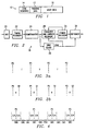
- Figure 1 illustrates such a frame designated generally at 10.
- frame 10 is a quadrature amplitude modulation ("QAM") frame, where it is known in the art that QAM frames encode data in an analog signal which includes one of a different available combination of phases and amplitudes to represent different bit patterns.
- training data 12 is provided within frame 10 to tune an equalizer in the receiving modem.
- frame 10 also includes a synchronization or "sync" sequence 14 placed at the start of frame 10.
- a receiving modem must recognize sync sequence 14 at some point during the receipt of frame 10.
- frame 10 includes user data 16 located after training data 12 and, thus, by locating the position of training data 12, the location of user data 16 also may be determined.
- FIG. 2 illustrates a block diagram of a receiver path in a modem 18.
- the block diagram of modem 18 is a general representation and, thus applies in general to the prior art but also may be modified as described later to form an inventive embodiment.
- Modem 18 receives frame data as an analog signal from a wireline (e.g., a telephone line or a cable, such as a coax cable), and that data is input to an analog-to digital converter (“ADC") 20 where it is converted to a digital form.
- ADC analog-to digital converter
- the digitally converted signal then passes to a timing recovery block 22 that re-times the sampling of the input waveform so that the receive sampling frequency tracks that of the transmitter in frequency.
- the signal passes to a demodulator 24 that removes the data from its modulated form, thereby producing the baseband values of the data.
- the frequency of the baseband value signal output from demodulator 24 is typically at some integer multiple (or other fraction greater than one) of the symbol rate; commonly, therefore, the output of demodulator 24 is at two times the symbol rate.
- the demodulated data passes to both a sync block 26 as well as an equalizer and carrier recovery block 28.
- Sync block 26 locates sync sequence 14 in each frame as detailed below, and when this location occurs sync block 26 asserts a SYNC signal to equalizer and carrier recovery block 28 so that it may synchronize itself to the incoming signal and perform training.
- Equalizer and carrier recovery block 28 outputs the equalized signal to a symbol decision block 30.
- Symbol decision block 30 performs the function of estimating the transmitted data from the output of equalizer and carrier recovery block 28. This is usually performed by finding the nearest point in the signal constellation to each received sample. This result is output to a deframer 32.
- symbol decision block 30 feeds back a signal to equalizer and carrier recover block 28 in order to provide decision-directed tracking of changes in the channel during the data portion of the frame.
- the SYNC signal from sync block 26 is also connected to deframer 32 so that it too may synchronize itself to the incoming signal. Further, deframer 32 performs the function of removing training data 12 and sync sequence 14 from frame 10, thereby leaving only user data 16.
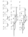
- sync block 26 locates sync sequence 14 in each frame 10 by taking periodic samples, where this approach is now described with the benefit of a general timing illustration in Figures 3a and 3b. Specifically, in Figure 3a, let the points P0 through P3 represent successive ideal sample locations in sync sequence 14, with a common time period T between each location.
- sync block 26 would sample the incoming signal at the exact point in time corresponding to point P0; in the art, this point is sometimes referred to as the center of a so-called eye diagram, with it understood that an actual sample taken at this ideal point is most likely to result in proper synchronization, and any increase in time between this ideal point and the actual sample point correspondingly decreases the synchronization performance (i.e., decreases the chance of successful synchronization). Additionally, given the sampling period T, sync block 26 then also ideally samples at each interval of T thereafter, thereby sampling exactly at the points P1, P2, and P3 illustrated in Figure 3a.
- FIG. 3b again illustrates points P0 through P3, and further illustrates a first scenario where a first actual sample S0 is taken, followed thereafter by additional samples at each period of T thereafter.
- samples are taken at times represented as S0, S1, S2, and S3.
- a technique is used whereby the samples are convolved with a filter correlation sequence that represents a time reversed, complex conjugate of sync sequence 14.
- the convolution determination will peak when sync sequence 14 is aligned with the filter correlation sequence.
- sync sequence 14 is typically formed by selecting from the four highest energy points of the symbol constellation and, indeed, using only the two of those four points that have the greatest spectral distance between them (i.e., -15-j max , +15+j max for QAM).
- the convolution peak may be detected by comparing the convolution result against a threshold, where the threshold is set to a level just below the anticipated maximum peak. Accordingly, when the threshold is exceeded, sync block 26 asserts its SYNC output, thereby informing other blocks in Figure 2 that synchronization has occurred.
- a length of time (or phase shift), indicated in Figure 3b as ⁇ occurs between each ideal sampling point and a corresponding actual sample.
- ⁇ is a length representing a distance between the ideal sampling time and the actual sampling time.
- the peak of the convolution may be less than the anticipated peak.
- the threshold used for comparison is lowered to accommodate the lower corresponding peak.
- the threshold is set too low, then it may be exceeded in some instances when an actual sync sequence has not been detected, which in turn could cause errant assertions of the SYNC output of sync block 26. Quite clearly, these errant assertions of the SYNC output may cause wrongful interpretation of incoming data.
- ⁇ max a maximum value of ⁇ , designated from this point forward as ⁇ max , may be determined empirically under which proper synchronization detection is ensured (or at least expected to meet an accepted confidence level).
- ⁇ max is determined empirically to equal T/4.
- Figure 4 once more illustrates points P0 through P3. Additionally, because ⁇ max equals T/4, then proper operation should occur so long as the sample for each point occurs within a time period no greater than T/4 before or after each such point.
- a sampling window of time having a period from T/4 before the point to T/4 after the point is shown with respect to each of points P0 through P3, labeled for reference as SW0 through SW3, respectively.
- SW0 through SW3 there also are periods of time that do not fall within these sampling widows. Given the preceding definitions, therefore, these periods of time represent instances where, if sampling occurs, proper sync detection may not occur.
- These periods are shown as error windows EW0 through EW3 in Figure 4. Note that each error window occurs beyond both edges of the sample window, that is, because the sample window is by definition centered about the point, then each point will have two corresponding error windows, one before and one after the sample window. Thus, in Figure 4, it is noted that the second instance of error window EW0 following point P0 coincides with a first instance of error window EW1 preceding point P1. A similar observation may be made regarding the remaining sample and error windows.
- the present inventor notes that the prior art may provide various drawbacks. For example, for a given system, if ⁇ max is relatively short, then the error windows EW0 through EW3 are relatively large. Accordingly, the chance of the periodic samples falling within error windows EW0 through EW3 are likewise increased, thereby increasing the likelihood of faulty sync detection, where faults may include both errant indication of synchronization or a total failure to achieve synchronization. Certain attempts may be made to reduce the chances of error by increasing the length of ⁇ max , such as by increasing the number of symbols in sync sequence 14. However, such an approach thereby reduces the bandwidth available for user data and, thus, may be undesirable. Consequently, this as well as other efforts may require greater resources (and cost), or simply may not be acceptable or feasible in various contexts. As a result, there arises a need to address the drawbacks of the prior art, as is achieved by the embodiments described below.
- the modem comprises circuitry for receiving an analog signal from a line and circuitry for converting the analog signal to a digital signal.
- the digital signal comprises a plurality of ideal sample points, each separated in time by a period T, and the plurality of ideal sample points comprises a sync sequence.
- the modem further comprises circuitry for detecting the sync sequence, comprising an integer number S of sampling circuits, where S is two or greater.
- Each of the sampling circuits comprises circuitry for taking a sample corresponding to each of the plurality of ideal sample points at least once per the period T.
- Each of the sampling circuits also comprises circuitry for comparing a plurality of taken samples to a correlation sequence.
- each of the sampling circuits comprises circuitry for outputting a sync detected signal in response to a sufficient match between the plurality of taken samples and the correlation sequence.
- FIG. 5 illustrates a block diagram of an inventive sync block 34.
- sync block 34 may be used in lieu of sync block 26 in Figure 2 to thereby form an inventive embodiment.
- sync block 34 of Figure 5 may be implemented in other wireline modems as well. In any event, any of the improved modems should provide more efficient frame synchronization functionality.
- sync block 34 includes a data input 36 for receiving the demodulated incoming data frames, where those frames are coupled to the input of two different correlators. More particularly, each incoming frame is coupled to a phase 0 correlator 38 and a phase 1 correlator 40. Each phase correlator samples the incoming frame and provides a synchronization ("sync") detected signal to a corresponding input of a post processor 42; for purposes of reference, the sync detected signal provided by phase 0 correlator 38 is identified as SYNC 0 and the sync detected signal provided by phase 1 correlator 40 is identified as SYNC 1 .
- sync synchronization
- Post processor 42 outputs a final sync detected signal, SYNC F , which is usable by various other devices within the modem implementing sync block 34 for purposes of synchronization.
- SYNC F may be used to synchronize sequence and compare circuit 28 and deframer 32 so that they may perform the functions described earlier.
- Sync block 34 also includes a second input 44 for receiving the symbol rate clock, where that rate corresponds to the period T described earlier in connection with Figure 3a.
- Input 44 couples the symbol rate clock to the input of a clock generator 46.
- Clock generator 46 doubles the symbol rate clock, that is, it provides an output clock signal that has a frequency equal to 2/T. This output clock signal is used to clock each of the other illustrated blocks in sync block 34, thereby facilitating a dual sample operation as further detailed in the remaining discussion.
- Figure 6a illustrates ideal sample points P10 through P13 representing successive ideal samples in a sync sequence, again with a symbol period T between each bit.
- Figure 6a also illustrates actual samples S10 0 , S11 0 , S12 0 , and S13 0 taken by phase 0 correlator 38 in relation to ideal sample points P10 through P13, respectively.
- the "0" designation from phase 0 correlator 38 is used as subscript with these samples to illustrate that the samples correspond to phase 0 correlator 38.
- Figure 6a illustrates actual samples S10 1 , S11 1 , S12 1 , and S13 1 taken by phase 1 correlator 40 in relation to ideal sample points P10 through P13, respectively; here, the "1" designation from phase 1 correlator 40 is used as subscript with these actual samples.
- Figure 6a demonstrates that for each ideal sample point both correlators 38 and 40 take an actual sample corresponding thereto.
- phase 0 correlator 38 takes a sample S10 0 at some arbitrary time, and at a time T/2 thereafter phase 1 correlator 10 takes a sample S10 1 . Similar timing observations should thus be apparent for the remaining samples taken and illustrated in Figure 6a. Lastly in this regard, recall that the output of demodulator 24 is commonly at two times the symbol rate and, thus, there is no need to further adjust this signal in order to achieve the T/2 samples by correlators 38 and 40.
- Figure 6a also introduces an important aspect of the distance between alternating samples of correlators 38 and 40 with respect to the ideal sample points P10 through P13. More particularly, in Figure 6a note that the first sample S10 0 by phase 0 correlator 38 occurs at some arbitrary time with respect to ideal sample point P10, and a distance of ⁇ 0 therefore exists between the sample and the corresponding ideal sample point. Because the other samples by phase 0 correlator 38 are later taken at a frequency of 1/T, then in general for subsequent samples they too will be separated by a distance of ⁇ 0 from the corresponding ideal sample point.
- phase 1 correlator 40 samples at a period T/2 thereafter, then a fixed distance relationship is also established between each sample of phase 1 correlator 40 and a corresponding ideal sample point. This fixed distance is shown in Figure 6a as ⁇ 1 .
- ⁇ max may be empirically determined for a system and represents the greatest distance in time which may exist between an ideal sample point and an actual sample point while still permitting acceptable identification of the sync sequence.
- ⁇ max may be empirically determined for a system and represents the greatest distance in time which may exist between an ideal sample point and an actual sample point while still permitting acceptable identification of the sync sequence.
- below are explored several examples to illustrate the potential relationship of ⁇ max to ⁇ 0 and ⁇ 1 , and to thereby demonstrate a benefit of the preferred embodiment.
- Figure 6c also illustrates error windows EW10 through EW12.
- error windows represent the same notion introduced in Figure 4 earlier, that is, if a sample is taken during an error window, it does not provide satisfactory information for detection of the sync sequence. Indeed, in the present example, since ⁇ 1 is greater than ⁇ max , note that the samples S10 1 through S13 1 in Figure 6c fall inside of the error windows. As a result, for the current example the samples taken by phase 1 correlator 40 are not reliable for proper sync sequence detection. However, recall that the samples taken by phase 0 correlator 38 are acceptable for such detection.
- Figure 7 illustrates a different set of ideal sample points P20 through P23 in a sync sequence, along with samples S20 0 , S21 0 , S22 0 , and S23 0 taken by phase 0 correlator 38 and samples S20 1 , S21 1 , S22 1 , and S23 1 taken by phase 1 correlator 40.
- the arbitrary timing of taking the first sample S20 0 causes it to be at a distance ⁇ 0 from P20, where that distance is greater than the distance ⁇ 1 between sample S20 1 and P20.
- ⁇ max is determined to be greater than ⁇ 1 but less than ⁇ 0
- the samples taken by phase 1 correlator 40 provide proper sync sequence detection while the samples taken by phase 0 correlator 38 do not.
- the arbitrary timing of the Figure 7 example demonstrates an instance where the limitation provided by ⁇ max is more likely to exclude the usefulness of the samples taken by phase 0 correlator 38 rather than those taken by phase 1 correlator 40.
- correlators 38 and 40 may provide samples sufficient to detect a sync sequence. Indeed, given the operation as discussed thus far, if ⁇ max is equal to or greater than T/2, then in each instance at least one of the two correlators should take a sample within an acceptable sample window. This may be contrasted with the prior art, where only a value of ⁇ max equal to T would ensure a comparable result. Accordingly, given that ⁇ max may be much smaller than in the prior art while still providing sufficient results, note therefore that such a value of ⁇ max may be achieved with a much shorter sync sequence. This in turn reduces the complexity of each correlator and there is less bandwidth required for overhead, thereby leaving more bandwidth for other data (e.g., user data).
- sync block 34 including two correlators
- an alternative embodiment may be created with an integer S number of correlators where S exceeds two, and where each corresponding correlator takes its sample at a period of T/S apart from any other correlator.
- at least one of the S correlators should provide satisfactory samples so long as the value of ⁇ max is equal to or greater than T/S.
- the two correlators already described may be connected as previously illustrated, but clocked or operated such that each takes more than one sample per period T, thereby providing a total of at least four samples per period T.
- post processor 42 which, recall, in general receives the SYNC 0 and SYNC 1 outputs of the correlators, and in response outputs a final sync detected signal SYNC F .
- the preceding has illustrated that in certain instances, only one of phase 0 correlator 38 or phase 1 correlator 40 will sample within an appropriate sample window. In such an instance, then only that one correlator will assert its SYNC output. However, the preceding has further demonstrated that in other instances, such as where ⁇ max is greater than T/2, both correlators may assert their SYNC outputs.
- Post processor 42 therefore, provides additional functionality to address these various contingent scenarios, as discussed below.
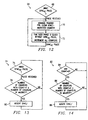
- post processor 42 begins with a step 50 where post processor 42 awaits a sync detected signal pulse from either phase 0 correlator 38 or phase 1 correlator 40. Thus, once either SYNC 0 or SYNC 1 is asserted, method 48 continues from the wait state of step 50 to step 52. Step 52 directs the remaining flow based on which of correlators 38 or 40 asserted its sync detected signal pulse.
- step 54 If the source of the asserted sync detected signal pulse is phase 0 correlator 38, method 48 continues to step 54; conversely, if the source of the asserted sync detected signal pulse is phase 1 correlator 40, method 48 continues to step 56.
- step 54 If the source of the asserted sync detected signal pulse is phase 0 correlator 38, method 48 continues to step 54; conversely, if the source of the asserted sync detected signal pulse is phase 1 correlator 40, method 48 continues to step 56.
- phase 0 correlator 38 i.e., the phase 0 clock
- phase 1 correlator 40 i.e., the phase 1 clock
- each rising edge of a phase clock causes its corresponding correlator to take a sample; thus, consistent with the earlier description, for a single period of the symbol clock, phase 0 correlator 38 takes a sample and at T/2 thereafter phase 1 correlator 40 takes a sample.
- phase 0 correlator 38 is clocked at t 0 , t 2 , t 4 , and so forth.
- Phase 1 correlator 40 is clocked at a time phase shifted by a duration of T/2 after phase 0 correlator 38 is clocked and, thus, for example, is clocked at t 1 , t 3 , t 5 , and so forth.
- step 54 an example of its occurrence is shown as occurring at time t 2 .
- the fourth and fifth rows in Figure 9 illustrate some examples of the SYNC 0 and SYNC 1 outputs, and at time t 2 it is seen that SYNC 0 is asserted.
- step 52 forwards method 48 to step 54, and step 54 asserts SYNC F during the same then current high state of the symbol clock, as shown at t 2 in the sixth row of Figure 9.
- phase 0 correlator 38 is considered a dominant correlator in that its assertion of SYNC 0 always causes an immediate corresponding assertion of SYNC F .
- step 56 having been reached by post processor 42 due to a received assertion of SYNC 1 , post processor 42 determines whether SYNC 0 was asserted for the current period of the symbol clock period (i.e., symbol clock high or low), that is, whether SYNC 0 was asserted at the time T/2 immediately before the current assertion of SYNC 1 . If this is the case, then SYNC F is not asserted and instead method 48 returns to step 50 and awaits the next asserted one of SYNC 0 or SYNC 1 . On the other hand, if SYNC 0 was not asserted at the time T/2 immediately before the current assertion of SYNC 1 , method 40 continues to step 58. Each of these alternative paths is analyzed below.
- step 58 method 48 returns to the wait state of step 50.
- FIG. 10 illustrates a block diagram of an alternative inventive sync block 34'.
- Sync block 34' includes all of the aspects of sync block 34 shown in Figure 5 and, thus, to demonstrate these like items, the same reference numerals are carried forward into Figure 10 and an apostrophe is added thereto.
- sync block 34' includes a second post processor identified generally at 60. More specifically, post processor 60 receives the synchronization signal from post processor 42' and, based on a method detailed below, outputs in various instances its own final sync detected signal, SYNC F ', where SYNC F ' may be connected to various other devices within the modem implementing sync block 34' for purposes of synchronization. To further illustrate this operation and by way of convention, for the Figure 10 embodiment the sync detected signal from post processor 42' is re-named from SYNC F to SYNC 42 to more easily distinguish it from SYNC F ' provided by post processor 60.
- post processor 60 includes a number of counters, with that number selected in a manner discussed later. For the present example, the number equals five and, thus, shown in Figure 11 are counters CTR1 through CTR5.
- Each counter is connected to receive the phase 0 clock signal (i.e., the dominant clock signal) and advances its count, in response to being clocked, from zero to an integer value equal to N-1, where for reasons detailed below N equals the number of clock cycles that should occur between synchronization detection (i.e., from the proper assertion of SYNC F ' to the next proper assertion of SYNC F ').
- post processor 60 includes a pointer PTR that is under the control of a pointer control circuit 62.
- pointer PTR moves in a circular fashion so that it points to a given counter and is then advanced to the next highest counter until it wraps around from counter CTR5 to counter CTR1.
- the values of the counts from each counter are connected as inputs to a counter evaluation circuit 64.
- Counter evaluation circuit 64 operates as detailed later to provide the final sync detected signal SYNC F '.
- post processor 60 The operation of post processor 60 is now discussed.
- the operation of post processor 60 in general is performed preferably in an effort to address a first situation, and may be further expanded in still another embodiment to address a second situation.
- the first situation preferably addressed by post processor 60 is to prevent a spurious assertion of SYNC 42 from reaching the other synchronizing components in the modem.
- the second situation that may be addressed by post processor 60 is to assert SYNC F ' to the other synchronizing components in the modem in the case where SYNC 42 should have been timely asserted but was not (i.e., neither SYNC 0 nor SYNC 1 was timely asserted).
- post processor 60 intercepts any spurious assertion of SYNC 42 in an effort to prevent it from reaching other modem components. More particularly, recall in connection with sync block 34 of Figure 5 that its SYNC F signal as provided by post processor 42 is used to synchronize various other modem circuits. However, it has been determined that various factors, such as noise, may cause an occasional spurious assertion of the sync detected signal from post processor 42 (here re-labeled as SYNC 42 ). Accordingly, in the alternative embodiment of sync block 34' in Figure 10, post processor 60 is added to respond to this event.
- post processor 60 determines that SYNC 42 was properly asserted, then the assertion is immediately translated into a corresponding assertion of SYNC F ' (e.g., by passing SYNC 42 through to SYNC F '). However, if post processor 60 determines that an assertion of SYNC 42 was spurious, then SYNC F ' is not correspondingly asserted. In the preferred embodiment, this aspect is achieved by monitoring the last integer M number of assertions of SYNC 42 and responding as explored in greater detail given the operation of pointer control circuit 62 and counter evaluation circuit 64.
- Method 66 commences with a wait state step 68, where pointer control circuit 62 awaits an assertion of SYNC 42 . During this time and all others, each of the counters advance in response to an assertions (e.g., rising edge) of the phase 0 clock. Once SYNC 42 is asserted, method 66 continues from the wait state of step 68 to step 70.
- step 70 pointer control circuit 62 advances pointer PTR so that it then points to the next higher numbered counter, or given the circular nature described above, if pointer PTR was pointing to counter CTR5 prior to step 70, then step 70 advances pointer PTR so that it then points to counter CTR1. In addition, step 70 clears the count in the newly identified counter.
- step 72 pointer control circuit 62 causes each of the counters to continue to increment for each phase 0 clock where there is no corresponding assertion of SYNC 42 .
- method 66 returns to step 70 so that the next counter is identified by pointer PTR and cleared, followed by a repeat of step 72 so that the next identified counter then counts upward starting from zero and in response to each phase 0 clock where there is no corresponding assertion of SYNC 42 , while the other counters likewise increment in response to the phase 0 clock.
- both counters CTR2 and CTR3 roll over to zero.
- SYNC 42 is asserted, thereby advancing pointer PTR to counter CTR4 and clearing it to zero. This process then continues for each counter so that once pointer PTR has cleared each counter and there have been proper assertions of SYNC 42 every 16 symbol (and phase 0) clocks, then at that point each counter stores a value equal to zero.
- the number of counters here equal to five, defines the amount of past history, that is, the number of most-recently asserted SYNC 42 signals, that are monitored by post processor 60.
- Method 74 commences with a start step 76, where counter evaluation circuit 64 awaits an assertion of SYNC 42 . Once SYNC 42 is asserted, method 74 continues from the wait state of step 76 to step 78. In step 78, counter evaluation circuit 64 determines whether the number of counters storing a value equal to zero is equal to or greater than the majority of the number of M counters.
- step 78 determines whether at least three counters store a value of zero If so, method 78 continues to step 80, whereas if not, method 78 returns to step 76.
- step 80 having been reached because at least a majority of counters store a value equal to zero, counter evaluation circuit 64 asserts SYNC F ' as corresponding to the asserted SYNC 42 received in step 76. Thereafter, method 74 returns to the wait state of step 76 until the next assertion of SYNC 42 .
- method 74 evaluates the counters to identify either normal operation (i.e., timely assertions of SYNC 42 ) as indicated by the equilibrium of either all or a majority of zero counts described above or, alternatively, to identify a potential spurious assertion of SYNC 42 when a majority of the counters do not reflect the above-described equilibrium. Further, when equilibrium or near-equilibrium is identified, then counter evaluation circuit 64 asserts SYNC F ' in response to a corresponding received assertion of SYNC 42 .
- counter evaluation circuit 64 merely receives the asserted SYNC 42 , but does not assert SYNC F ' so that the other synchronized modem components are not disturbed by this spurious event.
- post processor 60 may respond even if in fact SYNC 42 was not asserted.
- the response by post processor 60 is to insert an assertion of SYNC F ' in the appropriate time slot in an effort to maintain proper synchronization notwithstanding the fact that SYNC 42 was not timely asserted.
- this aspect is also achieved by monitoring the past history of SYNC 42 as represented by the last integer M number of assertions of SYNC 42 , and responding as explored in greater detail with reference to Figure 14.
- Figure 14 illustrates a flowchart of a method 82 which also may be included within the functionality of post processor 60 as introduced above.
- Method 82 commences with a step 84 that waits for the count in any of counters CTR1 through CTR5 to reach zero. When this occurs, method 82 continues from to step 86.
- step 86 counter evaluation circuit 64 determines whether the number of counters storing a value equal to zero is equal to or greater than the majority of the number of M counters. Thus, in the example of post processor 60 in Figure 11, step 86 determines whether at least three counters store a value of zero. If so, method 82 continues to step 88, whereas if not, method 82 returns to step 84.
- step 88 having been reached because at least a majority of counters store a value equal to zero, counter evaluation circuit 64 asserts SYNC F ' regardless of whether SYNC 42 was asserted in the same clock cycle that caused the counter to reach a count of zero from step 84. Thereafter, method 82 returns to the zero detection operation of step 84.
- method 82 evaluates the counters to identify an instance where SYNC 42 should have been asserted but was not, and responds by asserting a final sync signal SYNC F ' because it was expected that SYNC 42 should have been asserted. To further appreciate these operations, below are presented a few numeric examples.
- step 86 determines that the number of counters having a value of zero, which here is all five counters, is equal to or exceeds the number of counters in the majority (i.e., three). Consequently, method 82 continues to step 88 which asserts SYNC F '.
- SYNC F ' is asserted because it was anticipated, based on the past history of SYNC 42 assertions, that SYNC 42 should have been asserted during the current clock which thereby would have caused SYNC F ' to be asserted under method 74 of Figure 13. Accordingly, method 82 effectively inserts a SYNC F ' assertion where one might otherwise not have occurred because SYNC 42 was not asserted (i.e., because neither SYNC 0 nor SYNC 1 were asserted).
- the computer program is stored on a carrier medium in machine or device readable form, for example in solid-state memory or magnetic memory such as disc or tape and the processing device utilises the program or a part thereof to configure it for operation.
- the computer program may be supplied from a remote source embodied in a communications medium such as an electronic signal, radio frequency carrier wave or optical carrier wave.
- a communications medium such as an electronic signal, radio frequency carrier wave or optical carrier wave.
- carrier media are also envisaged as aspects of the present invention.
Abstract
Description
- The present embodiments relate to modems, and are more particularly, but not exclusively, directed to frame synchronization in wireline modems.
- The high-speed exchange of digital information between remotely located computers is now a pervasive part of modern computing in many contexts, including business, educational, and personal computer uses. It is contemplated that current and future applications of high speed data communications will continue the demand for systems and services in this field. For example, video on demand ("VOD") is one area which has for some time driven the advancement of technology in the area of digital information exchanges. More recently, the rapid increase in use and popularity of the Global Internet has further motivated research and preliminary development of systems directed to advanced communication of information between remotely located computers, particularly in accomplishing higher bit rates using existing infrastructure.
- Various types of modems have been and continue to be developed to achieve the high speed data communication arising from matters such as those described above. For example, ISDN modems typically transmit and receive data at speeds of 64 Kbps and 128 Kbps. As another example, cable modems are currently under development with the promise of data connections of much higher speeds than ISDN. More particularly, cable modems are anticipated to receive data at up to 10 Mbps and send data at speeds up from 2 to 10 Mbps. Still other modems are also known in the art.
- Given the proliferation of wireline modems, many such modems use frame structures to communicate information. By way of example, therefore, Figure 1 illustrates such a frame designated generally at 10. By way of example,
frame 10 is a quadrature amplitude modulation ("QAM") frame, where it is known in the art that QAM frames encode data in an analog signal which includes one of a different available combination of phases and amplitudes to represent different bit patterns. Withinframe 10 is providedtraining data 12 to tune an equalizer in the receiving modem. In order to locatetraining data 12,frame 10 also includes a synchronization or "sync"sequence 14 placed at the start offrame 10. As a result, a receiving modem must recognizesync sequence 14 at some point during the receipt offrame 10. Once this recognition occurs, it may be determined where the beginning of the frame is located, and it thus will be known where the end ofsync sequence 14 occurs. Knowing the location of the end ofsync sequence 14 thereby identifies the location of the beginning oftraining data 12. Additionally,frame 10 includesuser data 16 located aftertraining data 12 and, thus, by locating the position oftraining data 12, the location ofuser data 16 also may be determined. - By way of further background, Figure 2 illustrates a block diagram of a receiver path in a
modem 18. The block diagram ofmodem 18 is a general representation and, thus applies in general to the prior art but also may be modified as described later to form an inventive embodiment.Modem 18 receives frame data as an analog signal from a wireline (e.g., a telephone line or a cable, such as a coax cable), and that data is input to an analog-to digital converter ("ADC") 20 where it is converted to a digital form. The digitally converted signal then passes to atiming recovery block 22 that re-times the sampling of the input waveform so that the receive sampling frequency tracks that of the transmitter in frequency. Next, the signal passes to ademodulator 24 that removes the data from its modulated form, thereby producing the baseband values of the data. Note that the frequency of the baseband value signal output fromdemodulator 24 is typically at some integer multiple (or other fraction greater than one) of the symbol rate; commonly, therefore, the output ofdemodulator 24 is at two times the symbol rate. From the output ofdemodulator 24, the demodulated data passes to both async block 26 as well as an equalizer andcarrier recovery block 28.Sync block 26 locatessync sequence 14 in each frame as detailed below, and when this location occurssync block 26 asserts a SYNC signal to equalizer andcarrier recovery block 28 so that it may synchronize itself to the incoming signal and perform training. Equalizer andcarrier recovery block 28 outputs the equalized signal to asymbol decision block 30.Symbol decision block 30 performs the function of estimating the transmitted data from the output of equalizer andcarrier recovery block 28. This is usually performed by finding the nearest point in the signal constellation to each received sample. This result is output to adeframer 32. In addition,symbol decision block 30 feeds back a signal to equalizer and carrier recoverblock 28 in order to provide decision-directed tracking of changes in the channel during the data portion of the frame. Lastly, note that , the SYNC signal fromsync block 26 is also connected todeframer 32 so that it too may synchronize itself to the incoming signal. Further,deframer 32 performs the function of removingtraining data 12 and syncsequence 14 fromframe 10, thereby leaving onlyuser data 16. - Looking now to
sync block 26 in greater detail, it locatessync sequence 14 in eachframe 10 by taking periodic samples, where this approach is now described with the benefit of a general timing illustration in Figures 3a and 3b. Specifically, in Figure 3a, let the points P0 through P3 represent successive ideal sample locations insync sequence 14, with a common time period T between each location. In other words, in an ideal situation,sync block 26 would sample the incoming signal at the exact point in time corresponding to point P0; in the art, this point is sometimes referred to as the center of a so-called eye diagram, with it understood that an actual sample taken at this ideal point is most likely to result in proper synchronization, and any increase in time between this ideal point and the actual sample point correspondingly decreases the synchronization performance (i.e., decreases the chance of successful synchronization). Additionally, given the sampling period T,sync block 26 then also ideally samples at each interval of T thereafter, thereby sampling exactly at the points P1, P2, and P3 illustrated in Figure 3a. However, various factors causesync block 26 to take actual samples at a phase shifted point in time which is away from that of each point in Figure 3a. Such factors include the fact that there is no common clock or timing signal for synchronization between the transmitter and the receiver, and also may include other factors such as channel distortion and carrier errors. By way of example, therefore, Figure 3b again illustrates points P0 through P3, and further illustrates a first scenario where a first actual sample S0 is taken, followed thereafter by additional samples at each period of T thereafter. Thus, samples are taken at times represented as S0, S1, S2, and S3. As the samples are taken, a technique is used whereby the samples are convolved with a filter correlation sequence that represents a time reversed, complex conjugate ofsync sequence 14. As a result, the convolution determination will peak whensync sequence 14 is aligned with the filter correlation sequence. Also in this regard, in an effort to produce the greatest possible peak, note thatsync sequence 14 is typically formed by selecting from the four highest energy points of the symbol constellation and, indeed, using only the two of those four points that have the greatest spectral distance between them (i.e., -15-jmax, +15+jmax for QAM). Given these considerations, the convolution peak may be detected by comparing the convolution result against a threshold, where the threshold is set to a level just below the anticipated maximum peak. Accordingly, when the threshold is exceeded,sync block 26 asserts its SYNC output, thereby informing other blocks in Figure 2 that synchronization has occurred. - While the preceding approach may prove acceptable in some contexts, note further in Figure 3b that a length of time (or phase shift), indicated in Figure 3b as δ, occurs between each ideal sampling point and a corresponding actual sample. In other words, in Figure 3b δ is a length representing a distance between the ideal sampling time and the actual sampling time. Moreover, because of this time separation, note that the peak of the convolution may be less than the anticipated peak. As a result, under the prior art approach it may be required that the threshold used for comparison is lowered to accommodate the lower corresponding peak. However, if the threshold is set too low, then it may be exceeded in some instances when an actual sync sequence has not been detected, which in turn could cause errant assertions of the SYNC output of
sync block 26. Quite clearly, these errant assertions of the SYNC output may cause wrongful interpretation of incoming data. - Given the preceding, it has been recognized by the present inventor that the length of δ directly affects the likelihood that the prior art system will properly detect
sync sequence 14 in an incoming frame. Additionally, for systems of the type shown in Figure 2, a maximum value of δ, designated from this point forward as δmax, may be determined empirically under which proper synchronization detection is ensured (or at least expected to meet an accepted confidence level). To further illustrate this point, assume by way of example that δmax is determined empirically to equal T/4. This example is further illustrated in Figure 4. More particularly, Figure 4 once more illustrates points P0 through P3. Additionally, because δmax equals T/4, then proper operation should occur so long as the sample for each point occurs within a time period no greater than T/4 before or after each such point. To further illustrate these periods of anticipated proper operation, a sampling window of time having a period from T/4 before the point to T/4 after the point is shown with respect to each of points P0 through P3, labeled for reference as SW0 through SW3, respectively. Having defined sampling windows SW0 through SW3, there also are periods of time that do not fall within these sampling widows. Given the preceding definitions, therefore, these periods of time represent instances where, if sampling occurs, proper sync detection may not occur. These periods are shown as error windows EW0 through EW3 in Figure 4. Note that each error window occurs beyond both edges of the sample window, that is, because the sample window is by definition centered about the point, then each point will have two corresponding error windows, one before and one after the sample window. Thus, in Figure 4, it is noted that the second instance of error window EW0 following point P0 coincides with a first instance of error window EW1 preceding point P1. A similar observation may be made regarding the remaining sample and error windows. - From the above, the present inventor notes that the prior art may provide various drawbacks. For example, for a given system, if δmax is relatively short, then the error windows EW0 through EW3 are relatively large. Accordingly, the chance of the periodic samples falling within error windows EW0 through EW3 are likewise increased, thereby increasing the likelihood of faulty sync detection, where faults may include both errant indication of synchronization or a total failure to achieve synchronization. Certain attempts may be made to reduce the chances of error by increasing the length of δmax, such as by increasing the number of symbols in
sync sequence 14. However, such an approach thereby reduces the bandwidth available for user data and, thus, may be undesirable. Consequently, this as well as other efforts may require greater resources (and cost), or simply may not be acceptable or feasible in various contexts. As a result, there arises a need to address the drawbacks of the prior art, as is achieved by the embodiments described below. - In the preferred embodiment, there is a modem. The modem comprises circuitry for receiving an analog signal from a line and circuitry for converting the analog signal to a digital signal. The digital signal comprises a plurality of ideal sample points, each separated in time by a period T, and the plurality of ideal sample points comprises a sync sequence. The modem further comprises circuitry for detecting the sync sequence, comprising an integer number S of sampling circuits, where S is two or greater. Each of the sampling circuits comprises circuitry for taking a sample corresponding to each of the plurality of ideal sample points at least once per the period T. Each of the sampling circuits also comprises circuitry for comparing a plurality of taken samples to a correlation sequence. Finally, each of the sampling circuits comprises circuitry for outputting a sync detected signal in response to a sufficient match between the plurality of taken samples and the correlation sequence. Other circuits, systems, and methods are also disclosed and claimed.
- Embodiments in accordance with the invention will now be described by way of example only, and with reference to the accompanying drawings, in which:
- Figure 1 illustrates a frame of information communicated by a wireline modem;
- Figure 2 illustrates a block diagram of a receiving path in a wireline modem;
- Figure 3a illustrates a series of ideal sample points occurring in time, each separated by a same period T;
- Figure 3b illustrates the ideal sample points of Figure 3a with the addition of actual sample points taken relative to each of the ideal sample points;
- Figure 4 illustrates the ideal sample points of Figure 3a with the addition of sample windows and error windows defined relative thereto;
- Figure 5 illustrates a block diagram of a first embodiment of an improved synchronization block for use in a modem such as that shown in Figure 2 or in other wireline modems;
- Figure 6a illustrates a series of ideal sample points occurring in time, each separated by a same period T, and further illustrates two sets of actual sample points taken with respect to each of the ideal sample points;
- Figure 6b illustrates the points of Figure 6a given an example of a first system value δmax defining sample windows and error windows arising from a first instance of relative timing between the ideal sample points and the actual sample points of Figure 6a;
- Figure 6c illustrates the points of Figure 6a given an example of a second system value δmax defining sample windows and error windows arising from the first instance of relative timing between the ideal sample points and the actual sample points of Figure 6a;
- Figure 7 illustrates a series of ideal sample points occurring in time, where the two sets of actual sample points taken with respect to each ideal sample point occur such that a first actual sample point is taken before a corresponding ideal sample point and a second actual sample point is taken after the corresponding ideal sample point;
- Figure 8 illustrates a flow chart of the preferred method of operation of the sync block of Figure 5;
- Figure 9 illustrates a timing diagram of the operation of the sync block of Figure 5;
- Figure 10 illustrates a block diagram of a second embodiment of an improved synchronization block for use in a modem such as that shown in Figure 2 or in other wireline modems;
- Figure 11 illustrates a block diagram of the preferred
embodiment of
post processor 60 in Figure 10; - Figure 12 illustrates a flow chart of the method of
operation of
pointer control circuit 62 of Figure 11; - Figure 13 illustrates a flow chart of the method of
operation of
counter evaluation circuit 64 of Figure 11 to prevent a spurious sync detected signal from causing a final sync detected signal to reach various modem components; and - Figure 14 illustrates a flow chart of the method of
operation of
counter evaluation circuit 64 of Figure 11 to output a final sync detected signal in instances where sync detection did not occur but was anticipated to have occurred based on earlier timing history of prior sync detection events. -
- Figures 1 through 4 were discussed above by way of introduction and in some respects as relating to the prior art.
- Figure 5 illustrates a block diagram of an
inventive sync block 34. Before looking to the details ofsync block 34, first recall that it was earlier stated in connection withmodem 18 of Figure 2 that the block diagram therein may be modified to present an inventive embodiment. In this regard, the following provides a detailed discussion ofsync block 34, wheresync block 34 may be used in lieu ofsync block 26 in Figure 2 to thereby form an inventive embodiment. Alternatively,sync block 34 of Figure 5 may be implemented in other wireline modems as well. In any event, any of the improved modems should provide more efficient frame synchronization functionality. - Turning to the details of
sync block 34, it includes adata input 36 for receiving the demodulated incoming data frames, where those frames are coupled to the input of two different correlators. More particularly, each incoming frame is coupled to aphase 0correlator 38 and aphase 1correlator 40. Each phase correlator samples the incoming frame and provides a synchronization ("sync") detected signal to a corresponding input of apost processor 42; for purposes of reference, the sync detected signal provided byphase 0correlator 38 is identified as SYNC0 and the sync detected signal provided byphase 1correlator 40 is identified as SYNC1.Post processor 42 outputs a final sync detected signal, SYNCF, which is usable by various other devices within the modem implementingsync block 34 for purposes of synchronization. For example, whensync block 34 is implemented in a modem such asmodem 18 of Figure 2, SYNCF may be used to synchronize sequence and comparecircuit 28 anddeframer 32 so that they may perform the functions described earlier. -
Sync block 34 also includes asecond input 44 for receiving the symbol rate clock, where that rate corresponds to the period T described earlier in connection with Figure 3a.Input 44 couples the symbol rate clock to the input of aclock generator 46.Clock generator 46 doubles the symbol rate clock, that is, it provides an output clock signal that has a frequency equal to 2/T. This output clock signal is used to clock each of the other illustrated blocks insync block 34, thereby facilitating a dual sample operation as further detailed in the remaining discussion. - The operation of
sync block 34 is now explored. In general,phase 0correlator 38 andphase 1correlator 40 each periodically sample the information frominput 36, and each compares the sample against a reference pattern to locate an incoming sync sequence. This comparison may be achieved using convolution to compare the samples against a correlation sequence as described earlier with respect to the prior art, or through other methods ascertainable by one skilled in the art. Accordingly, one skilled in the art may develop various different circuit and related architectures for achieving this functionality given the art. In any event, when a sufficient match occurs between the sample and the corresponding sequence, such as may be determined by comparison against a threshold value or some other technique, the corresponding correlator asserts its output sync detected signal. Importantly for purposes of the present embodiment, however, is the timing of the samples taken byphase 0correlator 38 andphase 1correlator 40. This timing is explored below in connection with Figure 6a. - Figure 6a illustrates ideal sample points P10 through P13 representing successive ideal samples in a sync sequence, again with a symbol period T between each bit. Figure 6a also illustrates actual samples S100, S110, S120, and S130 taken by
phase 0correlator 38 in relation to ideal sample points P10 through P13, respectively. With respect to these actual samples, note that the "0" designation fromphase 0correlator 38 is used as subscript with these samples to illustrate that the samples correspond tophase 0correlator 38. In a similar manner, Figure 6a illustrates actual samples S101, S111, S121, and S131 taken byphase 1correlator 40 in relation to ideal sample points P10 through P13, respectively; here, the "1" designation fromphase 1correlator 40 is used as subscript with these actual samples. In general, therefore, and as explored below, Figure 6a demonstrates that for each ideal sample point bothcorrelators - Attention is now turned to the timing of the samples taken by
phase 0correlator 38 andphase 1correlator 40. In this regard, recall thatclock generator 46 outputs a clock signal having a frequency of 2/T. In response to this and as illustrated in Figure 6a, the samples taken byphase 0correlator 38 andphase 1correlator 40 alternate in sample operation so that for a given idealsample point phase 0correlator 38 first takes a sample and at a period, preferably of T/2, thereafterphase 1correlator 40 takes a sample. Looking to ideal sample point P10 by way of example,phase 0correlator 38 takes a sample S100 at some arbitrary time, and at a time T/2 thereafterphase 1correlator 10 takes a sample S101. Similar timing observations should thus be apparent for the remaining samples taken and illustrated in Figure 6a. Lastly in this regard, recall that the output ofdemodulator 24 is commonly at two times the symbol rate and, thus, there is no need to further adjust this signal in order to achieve the T/2 samples bycorrelators - Figure 6a also introduces an important aspect of the distance between alternating samples of
correlators phase 0correlator 38 occurs at some arbitrary time with respect to ideal sample point P10, and a distance of δ0 therefore exists between the sample and the corresponding ideal sample point. Because the other samples byphase 0correlator 38 are later taken at a frequency of 1/T, then in general for subsequent samples they too will be separated by a distance of δ0 from the corresponding ideal sample point. Once the arbitrary-timed first actual sample S100 byphase 0correlator 38 is taken, and becausephase 1correlator 40 then samples at a period T/2 thereafter, then a fixed distance relationship is also established between each sample ofphase 1correlator 40 and a corresponding ideal sample point. This fixed distance is shown in Figure 6a as δ1. - Having established the sample distances of δ0 and δ1, their benefit is now appreciated by recalling the concept of δmax and comparing it to the sample distances. Specifically, recall that δmax may be empirically determined for a system and represents the greatest distance in time which may exist between an ideal sample point and an actual sample point while still permitting acceptable identification of the sync sequence. Against this background, below are explored several examples to illustrate the potential relationship of δmax to δ0 and δ1, and to thereby demonstrate a benefit of the preferred embodiment.
- As a first example of the operation of
sync block 34, suppose that δmax for the system achieving the samples in Figure 6a is determined to be greater than δ1. To further illustrate this example, Figure 6b illustrates the ideal sample points and actual samples of Figure 6a and further illustrates sampling windows SW10 through SW12 oflength 2 * δ max centered about each respective ideal sample point (SW 13 is not shown for simplicity sake). Further, since both δ 0 and δ 1 are less than δ max, then either the sample byphase 0correlator 38 or the sample byphase 1correlator 40 fall within the sampling windows and, hence, should produce an acceptable identification of the sync sequence. - As a second example of the operation of
sync block 34, suppose that δmax for the system achieving the samples in Figure 6a is determined to be greater than δ0 but less than δ1. To further illustrate this example, Figure 6c illustrates the ideal sample points and actual sample points of Figure 6a and further illustrates sampling windows SW10 through SW12 oflength 2 * δmax centered about each respective ideal sample point (again,SW 13 is not shown for simplicity sake). In the present example, since δ0 is less than δmax, then samples S100 through S130 in Figure 6c fall inside the sample windows and, hence, the samples taken byphase 0correlator 38 may be used for proper sync sequence detection. In contrast, however, Figure 6c also illustrates error windows EW10 through EW12. These error windows represent the same notion introduced in Figure 4 earlier, that is, if a sample is taken during an error window, it does not provide satisfactory information for detection of the sync sequence. Indeed, in the present example, since δ1 is greater than δmax, note that the samples S101 through S131 in Figure 6c fall inside of the error windows. As a result, for the current example the samples taken byphase 1correlator 40 are not reliable for proper sync sequence detection. However, recall that the samples taken byphase 0correlator 38 are acceptable for such detection. Accordingly, from the example of Figure 6c it now should be appreciated that the method of taking dual samples per ideal sample point, as is achieved bysync block 34, significantly increases the possibility that at least one of the two correlators will obtain a set of satisfactory samples for proper sync sequence detection. This result is further illustrated below. - While the preceding example illustrates an instance where
phase 0correlator 38 produces acceptable samples whilephase 1correlator 40 does not, note that such a result arises due to the arbitrary location of the first sample S100 relative to the location in time of ideal sample point P10. To further illustrate this aspect, Figure 7 illustrates a different set of ideal sample points P20 through P23 in a sync sequence, along with samples S200, S210, S220, and S230 taken byphase 0correlator 38 and samples S201, S211, S221, and S231 taken byphase 1correlator 40. In this example, the arbitrary timing of taking the first sample S200 causes it to be at a distance δ0 from P20, where that distance is greater than the distance δ1 between sample S201 and P20. In this example, therefore, if δmax is determined to be greater than δ1 but less than δ0, then the samples taken byphase 1correlator 40 provide proper sync sequence detection while the samples taken byphase 0correlator 38 do not. In other words, the arbitrary timing of the Figure 7 example demonstrates an instance where the limitation provided by δmax is more likely to exclude the usefulness of the samples taken byphase 0correlator 38 rather than those taken byphase 1correlator 40. - Having demonstrated the general operation of
correlators - Having described a preferred embodiment of
sync block 34 including two correlators, an alternative embodiment may be created with an integer S number of correlators where S exceeds two, and where each corresponding correlator takes its sample at a period of T/S apart from any other correlator. Under this approach, at least one of the S correlators should provide satisfactory samples so long as the value of δmax is equal to or greater than T/S. Alternatively, the two correlators already described may be connected as previously illustrated, but clocked or operated such that each takes more than one sample per period T, thereby providing a total of at least four samples per period T. In any event, therefore, even for systems with relatively low values of δmax they may be made to provide satisfactory results by providing a sufficient number of correlators or correlator samples according to the principles discussed above. Still further, as N continues to increase, the necessary value of δmax decreases and, as stated above for the case of two correlators, the smaller value of δmax increases the bandwidth available for user data and simplifies the complexity of each correlator. - Additional discussion is now directed to post
processor 42 which, recall, in general receives the SYNC0 and SYNC1 outputs of the correlators, and in response outputs a final sync detected signal SYNCF. Specifically, the preceding has illustrated that in certain instances, only one ofphase 0correlator 38 orphase 1correlator 40 will sample within an appropriate sample window. In such an instance, then only that one correlator will assert its SYNC output. However, the preceding has further demonstrated that in other instances, such as where δmax is greater than T/2, both correlators may assert their SYNC outputs.Post processor 42, therefore, provides additional functionality to address these various contingent scenarios, as discussed below. - The operation of
post processor 42 is now described by way of amethod 48 shown in flow chart form in Figure 8, and further with reference to a sample timing diagram in Figure 9. Looking first to Figure 8,method 48 begins with astep 50 wherepost processor 42 awaits a sync detected signal pulse from eitherphase 0correlator 38 orphase 1correlator 40. Thus, once either SYNC0 or SYNC1 is asserted,method 48 continues from the wait state ofstep 50 to step 52.Step 52 directs the remaining flow based on which ofcorrelators phase 0correlator 38,method 48 continues to step 54; conversely, if the source of the asserted sync detected signal pulse isphase 1correlator 40,method 48 continues to step 56. Each of these alternative paths is discussed below. - In
step 54, having been reached bypost processor 42 due to a received assertion of SYNC0,post processor 42 responds by asserting SYNCF during the current high state of the symbol clock. An example of this operation is shown with reference to Figure 9. Specifically, the top row of Figure 9 illustrates the symbol clock as input toclock generator 46, where recall that clock has a period equal to T. It is contemplated that the rising edge of the symbol clock causes operation ofmodem 18 in general, but of course an alternative embodiment could be constructed given the present teachings where the devices are triggered on a falling clock edge. The second and third rows of Figure 9 illustrate the resulting clock signals applied tophase 0 correlator 38 (i.e., thephase 0 clock) andphase 1 correlator 40 (i.e., thephase 1 clock), respectively. Further with respect to these second and third rows, note that each rising edge of a phase clock causes its corresponding correlator to take a sample; thus, consistent with the earlier description, for a single period of the symbol clock,phase 0correlator 38 takes a sample and at T/2 thereafterphase 1correlator 40 takes a sample. For example,phase 0correlator 38 is clocked at t0, t2, t4, and so forth.Phase 1correlator 40 is clocked at a time phase shifted by a duration of T/2 afterphase 0correlator 38 is clocked and, thus, for example, is clocked at t1, t3, t5, and so forth. Returning now to the operation ofstep 54, an example of its occurrence is shown as occurring at time t2. Particularly, the fourth and fifth rows in Figure 9 illustrate some examples of the SYNC0 and SYNC1 outputs, and at time t2 it is seen that SYNC0 is asserted. Thus, step 52forwards method 48 to step 54, and step 54 asserts SYNCF during the same then current high state of the symbol clock, as shown at t2 in the sixth row of Figure 9. In this regard, it should be noted thatphase 0correlator 38 is considered a dominant correlator in that its assertion of SYNC0 always causes an immediate corresponding assertion of SYNCF. - Alternatively in
step 56, having been reached bypost processor 42 due to a received assertion of SYNC1,post processor 42 determines whether SYNC0 was asserted for the current period of the symbol clock period (i.e., symbol clock high or low), that is, whether SYNC0 was asserted at the time T/2 immediately before the current assertion of SYNC1. If this is the case, then SYNCF is not asserted and insteadmethod 48 returns to step 50 and awaits the next asserted one of SYNC0 or SYNC1. On the other hand, if SYNC0 was not asserted at the time T/2 immediately before the current assertion of SYNC1,method 40 continues to step 58. Each of these alternative paths is analyzed below. - Turning first to the example of flow from
step 56 back to step 50, recall this occurs when SYNC0 was asserted at the time T/2 immediately before the current assertion of SYNC1. To further appreciate the effect of this flow, an example of this situation occurs at t3 in Figure 9. Specifically, at t3 it is seen that SYNC1 is asserted. Moreover, at the time T/2 immediately prior, that is, at t2, SYNC0 was asserted. Thus, at time t3 there is no assertion of SYNCF. Due to this operation, therefore, SYNCF is only asserted at t2 (because of the assertion of SYNC0), and it is not again asserted immediately thereafter at t3. In operating in this manner, therefore, note that even when both SYNC0 and SYNC1 have been asserted in consecutive cycles, only a single assertion of a sync detected signal pulse, SYNCF, is allowed to reach other circuits requiring synchronization in the modem. Consequently, there is an avoidance of any lock-up or wrongful action which could otherwise occur if two sync pulses were consecutively issued and used to trigger attempts by other circuits to synchronize to the incoming frame. Lastly, following the completion ofstep 54,method 48 returns to the wait state ofstep 50. - Turning second to the example of flow from
step 56 continuing to step 58, recall this occurs when SYNC1 was asserted and SYNC0 was not asserted at the time T/2 immediately before the current assertion of SYNC1. To further appreciate the effect of this flow, an example of this situation occurs at t7 in Figure 9. Specifically, at t7 it is seen that SYNC1 is asserted, and at the time T/2 immediately prior (i.e., t6), SYNC0 was not asserted. In response, step 58 asserts SYNCF during the next high state of the symbol clock. Accordingly, SYNCF is only asserted at t8, which therefore corresponds to the rising edge and high state of the symbol clock. In operating in this manner, therefore, note that this or the earlier-described assertion of SYNCF always occurs only on a high state of the symbol clock. Accordingly, SYNCF is only asserted at the same clock edge (i.e., the rising edge of the symbol clock) as that used for other devices clocked by the symbol clock, which thereby ensures more consistent operation by the devices receiving the SYNCF signal. Lastly, following the completion ofstep 58,method 48 returns to the wait state ofstep 50. - Figure 10 illustrates a block diagram of an alternative inventive sync block 34'. Sync block 34' includes all of the aspects of
sync block 34 shown in Figure 5 and, thus, to demonstrate these like items, the same reference numerals are carried forward into Figure 10 and an apostrophe is added thereto. In addition, however, sync block 34' includes a second post processor identified generally at 60. More specifically,post processor 60 receives the synchronization signal from post processor 42' and, based on a method detailed below, outputs in various instances its own final sync detected signal, SYNCF', where SYNCF' may be connected to various other devices within the modem implementing sync block 34' for purposes of synchronization. To further illustrate this operation and by way of convention, for the Figure 10 embodiment the sync detected signal from post processor 42' is re-named from SYNCF to SYNC42 to more easily distinguish it from SYNCF' provided bypost processor 60. - The operation of
post processor 60 is explored later, with reference first made to Figure 11 which illustrates a block diagram ofpost processor 60 in detail. In the preferred embodiment,post processor 60 includes a number of counters, with that number selected in a manner discussed later. For the present example, the number equals five and, thus, shown in Figure 11 are counters CTR1 through CTR5. Each counter is connected to receive thephase 0 clock signal (i.e., the dominant clock signal) and advances its count, in response to being clocked, from zero to an integer value equal to N-1, where for reasons detailed below N equals the number of clock cycles that should occur between synchronization detection (i.e., from the proper assertion of SYNCF' to the next proper assertion of SYNCF'). This time is known since it relates to the number of symbols inframe 10. Once a counter reaches N-1, on its next clock it rolls over to a value of zero, and thereafter it repeats the advancement just described toward a value of N-1. In addition,post processor 60 includes a pointer PTR that is under the control of apointer control circuit 62. The detailed operation ofpointer control circuit 62 is discussed below, but at this point it is noted pointer PTR moves in a circular fashion so that it points to a given counter and is then advanced to the next highest counter until it wraps around from counter CTR5 to counter CTR1. The values of the counts from each counter are connected as inputs to acounter evaluation circuit 64.Counter evaluation circuit 64 operates as detailed later to provide the final sync detected signal SYNCF'. - The operation of
post processor 60 is now discussed. By way of introduction, the operation ofpost processor 60 in general is performed preferably in an effort to address a first situation, and may be further expanded in still another embodiment to address a second situation. The first situation preferably addressed bypost processor 60 is to prevent a spurious assertion of SYNC42 from reaching the other synchronizing components in the modem. The second situation that may be addressed bypost processor 60 is to assert SYNCF' to the other synchronizing components in the modem in the case where SYNC42 should have been timely asserted but was not (i.e., neither SYNC0 nor SYNC1 was timely asserted). Each of these two situations is discussed below. - The first of the operational aspects of
post processor 60 is now introduced in general. In one aspect,post processor 60 intercepts any spurious assertion of SYNC42 in an effort to prevent it from reaching other modem components. More particularly, recall in connection withsync block 34 of Figure 5 that its SYNCF signal as provided bypost processor 42 is used to synchronize various other modem circuits. However, it has been determined that various factors, such as noise, may cause an occasional spurious assertion of the sync detected signal from post processor 42 (here re-labeled as SYNC42). Accordingly, in the alternative embodiment of sync block 34' in Figure 10,post processor 60 is added to respond to this event. More particularly, to the extent that postprocessor 60 determines that SYNC42 was properly asserted, then the assertion is immediately translated into a corresponding assertion of SYNCF' (e.g., by passing SYNC42 through to SYNCF'). However, ifpost processor 60 determines that an assertion of SYNC42 was spurious, then SYNCF' is not correspondingly asserted. In the preferred embodiment, this aspect is achieved by monitoring the last integer M number of assertions of SYNC42 and responding as explored in greater detail given the operation ofpointer control circuit 62 andcounter evaluation circuit 64. - The counter maintenance aspect of
pointer control circuit 62 is now described in detail by way of amethod 66 shown in flow chart form in Figure 12.Method 66 commences with await state step 68, wherepointer control circuit 62 awaits an assertion of SYNC42. During this time and all others, each of the counters advance in response to an assertions (e.g., rising edge) of thephase 0 clock. Once SYNC42 is asserted,method 66 continues from the wait state ofstep 68 to step 70. Instep 70,pointer control circuit 62 advances pointer PTR so that it then points to the next higher numbered counter, or given the circular nature described above, if pointer PTR was pointing to counter CTR5 prior to step 70, then step 70 advances pointer PTR so that it then points to counter CTR1. In addition,step 70 clears the count in the newly identified counter. Next, instep 72,pointer control circuit 62 causes each of the counters to continue to increment for eachphase 0 clock where there is no corresponding assertion of SYNC42. However, once there is aphase 0 clock along with an assertion of SYNC42, thenmethod 66 returns to step 70 so that the next counter is identified by pointer PTR and cleared, followed by a repeat ofstep 72 so that the next identified counter then counts upward starting from zero and in response to eachphase 0 clock where there is no corresponding assertion of SYNC42, while the other counters likewise increment in response to thephase 0 clock. - To further demonstrate the operation of
method 66, assume by way of a numerical example that under normal and proper operations, there are 16 assertions of the symbol clock between each proper synchronization event. In other words, under proper sync detection, SYNC42 is asserted every 16 symbol clocks and, thus, every 16phase 0 clocks. Further, recall that N equals the number of symbol clocks between sync detections and, hence, each of counters CTR1 through CTR5 counts from zero up to a value of 15 (i.e., N-1), and on the next clock to a given counter it rolls over to a value of zero to once again count upward from that value. From these assumptions, it is now demonstrated that under propersync operation method 66 produces a result that at some point each of counters CTR1 through CTR5 stores a value of zero. More particularly, assume at start up thatmethod 66 is in the wait state ofstep 68 and that pointer PTR points to counter CTR1 during this time. Next, assume SYNC42 is asserted. At this point, pointer PTR advances to identify counter CTR2 and that counter is cleared. Next, for each assertion of thephase 0 clock where SYNC42 is not asserted, counter CTR2 increments. Thus, given the present example, for the next 15 assertions of thephase 0 clock, counter CTR2 increments, thereby resulting in it storing a counter equal to 15. For the very next assertion of thephase 0 clock where SYNC42 is not asserted, counter CTR2 rolls over to store a value equal to 0. Continuing with the normal operation, on the next assertion of thephase 0 clock, SYNC42 is asserted, thereby advancing pointer PTR to counter CTR3 and clearing that counter. Next, there are 15phase 0 clocks without an assertion of SYNC42, where each correspondingly increments counter CTR3. At the same time, these same 15phase 0 clocks are incrementing counter CTR2 (as well as the other counters). Thus, both counters CTR2 and CTR3 each have the same count at a given time, somewhere between 0 and 15. On thesixteenth phase 0 clock, both counters CTR2 and CTR3 roll over to zero. At the same time, however, under proper operations, SYNC42 is asserted, thereby advancing pointer PTR to counter CTR4 and clearing it to zero. This process then continues for each counter so that once pointer PTR has cleared each counter and there have been proper assertions of SYNC42 every 16 symbol (and phase 0) clocks, then at that point each counter stores a value equal to zero. Lastly, it now should be appreciated that the number of counters, here equal to five, defines the amount of past history, that is, the number of most-recently asserted SYNC42 signals, that are monitored bypost processor 60. - The preceding discussion of normal operations and the resulting counts provides a background to appreciate the first aspect of the preferred operation of
counter evaluation circuit 64 which is now described by way of amethod 74 shown in flow chart form in Figure 13.Method 74 commences with astart step 76, wherecounter evaluation circuit 64 awaits an assertion of SYNC42. Once SYNC42 is asserted,method 74 continues from the wait state ofstep 76 to step 78. Instep 78,counter evaluation circuit 64 determines whether the number of counters storing a value equal to zero is equal to or greater than the majority of the number of M counters. Thus, in the example ofpost processor 60 in Figure 11,step 78 determines whether at least three counters store a value of zero If so,method 78 continues to step 80, whereas if not,method 78 returns to step 76. Instep 80, having been reached because at least a majority of counters store a value equal to zero,counter evaluation circuit 64 asserts SYNCF' as corresponding to the asserted SYNC42 received instep 76. Thereafter,method 74 returns to the wait state ofstep 76 until the next assertion of SYNC42. - Given the above description of Figure 13, it now may be appreciated that
method 74 evaluates the counters to identify either normal operation (i.e., timely assertions of SYNC42) as indicated by the equilibrium of either all or a majority of zero counts described above or, alternatively, to identify a potential spurious assertion of SYNC42 when a majority of the counters do not reflect the above-described equilibrium. Further, when equilibrium or near-equilibrium is identified, then counterevaluation circuit 64 asserts SYNCF' in response to a corresponding received assertion of SYNC42. Alternatively, when a potential spurious assertion of SYNC42 is identified, then counterevaluation circuit 64 merely receives the asserted SYNC42, but does not assert SYNCF' so that the other synchronized modem components are not disturbed by this spurious event. To further appreciate these operations, below are presented a few numeric examples. - As a first example of the operation of
counter evaluation circuit 64 permethod 74, recall the preceding example where N equals 16 and assume that complete equilibrium is achieved, that is, all counters are on track to reach a value of zero on the next assertion of SYNC42. For example, assume that counter CTR2 is currently identified by pointer PTR and has a value of 12, and all counters other than counter CTR2 also store a value of 12, as shown in Table 1.1:CTR
1CTR
2CTR
3CTR
4CTR
512 12 12 12 12 more phase 0 clocks without an assertion of SYNC42. At this point, therefore, the value of the counters are as shown below in Table 1.2:CTR
1CTR
2CTR
3CTR
4CTR
515 15 15 15 15 next phase 0 clock, assume SYNC42 is asserted. Accordingly, each counter rolls over to a value of zero, pointer PTR moves from counter CTR2 to counter CTR3 andcounter CTR 3 is cleared, and counterevaluation circuit 64 moves fromstep 76 to step 78. Further, since all counters then equal zero, the flow continues to step 80. Consequently, instep 80, in response to the received assertion of SYNC42,counter evaluation circuit 64 provides a corresponding assertion of SYNCF'. In effect, therefore, the asserted SYNC42 is merely passed onward in the form of the asserted SYNCF'. - As a second example of the operation of
counter evaluation circuit 64 permethod 74, assume now that counter CTR1 is currently identified by pointer PTR, and due to the five most recent assertions of SYNC42, the counts in counters CTR1 through CTR5 are as shown in Table 2.1:CTR
1CTR
2CTR
3CTR
4CTR
512 12 12 12 12 - Next, assume that SYNC42 is asserted during the
next phase 0 clock. Accordingly, pointer PTR advances to counter CTR2 which is then cleared, and at this point the counts in counters CTR1 through CTR5 are as shown in Table 2.2:CTR
1CTR
2CTR
3CTR
4CTR
513 0 13 13 13 counter evaluation circuit 64 moves fromstep 76 to step 78, and since the majority of the counters do not then equal zero, then the flow returns to step 76. As a result,step 80 is not reached and SYNCF' is not asserted. In other words, it has been detected at this point that the assertion of SYNC42 was a spurious assertion and, as a result, no final synchronization signal SYNCF' is allowed to reach the other synchronized components of the modem. - Turning now to an additional aspect of the operation of
post processor 60, various factors also may cause SYNC42 not to be asserted when in fact it should be asserted, that is, when the anticipated time for SYNC42 to have been asserted occurs,post processor 60 may respond even if in fact SYNC42 was not asserted. In general, the response bypost processor 60 is to insert an assertion of SYNCF' in the appropriate time slot in an effort to maintain proper synchronization notwithstanding the fact that SYNC42 was not timely asserted. In the preferred embodiment, this aspect is also achieved by monitoring the past history of SYNC42 as represented by the last integer M number of assertions of SYNC42, and responding as explored in greater detail with reference to Figure 14. - Figure 14 illustrates a flowchart of a
method 82 which also may be included within the functionality ofpost processor 60 as introduced above.Method 82 commences with astep 84 that waits for the count in any of counters CTR1 through CTR5 to reach zero. When this occurs,method 82 continues from to step 86. Instep 86,counter evaluation circuit 64 determines whether the number of counters storing a value equal to zero is equal to or greater than the majority of the number of M counters. Thus, in the example ofpost processor 60 in Figure 11,step 86 determines whether at least three counters store a value of zero. If so,method 82 continues to step 88, whereas if not,method 82 returns to step 84. Instep 88, having been reached because at least a majority of counters store a value equal to zero,counter evaluation circuit 64 asserts SYNCF' regardless of whether SYNC42 was asserted in the same clock cycle that caused the counter to reach a count of zero fromstep 84. Thereafter,method 82 returns to the zero detection operation ofstep 84. - Given the above description of Figure 14, it now may be appreciated that
method 82 evaluates the counters to identify an instance where SYNC42 should have been asserted but was not, and responds by asserting a final sync signal SYNCF' because it was expected that SYNC42 should have been asserted. To further appreciate these operations, below are presented a few numeric examples. - As a first example of the operation of
counter evaluation circuit 64 permethod 82, recall again the preceding example where N equals 16 and assume that complete equilibrium is achieved, that is, all counters are on track to reach a value of zero on the next assertion of SYNC42. For example, assume that counter CTR3 is currently identified by pointer PTR and has a value of 14, and all counters other than counter CTR3 also store a value of 14, as shown in Table 3.1:CTR
1CTR
2CTR
3CTR
4CTR
514 14 14 14 14 - Next, assume that two
more phase 0 clocks are asserted, but SYNC42 is not asserted. At this point, therefore, pointer PTR does not advance but instead it continues to point to counter CTR3. However, the twoadditional phase 0 clocks have now caused all of the counters to roll to zero, as shown in the Table 3.2:CTR
1CTR
2CTR
3CTR
4CTR
50 0 0 0 0 - Given the instance illustrated by Table 3.2,
method 82 moves fromstep 84 to step 86 because at least one count equals zero. Further,step 86 determines that the number of counters having a value of zero, which here is all five counters, is equal to or exceeds the number of counters in the majority (i.e., three). Consequently,method 82 continues to step 88 which asserts SYNCF'. Thus, even though SYNC42 was not asserted, undermethod 82 of Figure 14 SYNCF' is asserted because it was anticipated, based on the past history of SYNC42 assertions, that SYNC42 should have been asserted during the current clock which thereby would have caused SYNCF' to be asserted undermethod 74 of Figure 13. Accordingly,method 82 effectively inserts a SYNCF' assertion where one might otherwise not have occurred because SYNC42 was not asserted (i.e., because neither SYNC0 nor SYNC1 were asserted). - From the above, it may be appreciated that the above embodiments provide improved operation for synchronization in a wireline modem. Moreover, while the present embodiments have been described in detail, various substitutions, modifications or alterations could be made to the descriptions set forth above without departing from the inventive scope. For example, many of the various blocks set forth herein are defined in terms of their functionality and, thus, one skilled in the art may choose various forms to implement that functionality. For example, some or all of the functionality provided may be embodied using a single digital signal processor, or in alternative circuits such as in an application specific integrated circuit or a larger circuit that forms other aspects of the modem functionality. As still another example, while separate sampling -circuits have been shown to achieve multiple actual samples per each ideal sample point, a single circuit could be constructed to take such multiple samples with additional circuitry to then evaluate those samples consistent with the methodologies described herein. In any event, these examples as well as others discussed earlier and those ascertainable by one skilled in the art further develop the inventive scope, as is defined by the following claims.
- Insofar as embodiments of the invention described above are implementable, at least in part, using a software-controlled programmable processing device such as a Digital Signal Processor, microprocessor or other processing device, it will be appreciated that a computer program for configuring the programmable device to implement the foregoing described methods is envisaged as an aspect of the present invention.
- Suitably, the computer program is stored on a carrier medium in machine or device readable form, for example in solid-state memory or magnetic memory such as disc or tape and the processing device utilises the program or a part thereof to configure it for operation. The computer program may be supplied from a remote source embodied in a communications medium such as an electronic signal, radio frequency carrier wave or optical carrier wave. Such carrier media are also envisaged as aspects of the present invention.
- The scope of the present disclosure includes any novel feature or combination of features disclosed therein either explicitly or implicitly or any generalisation thereof irrespective of whether or not it relates to the claimed invention or mitigates any or all of the problems addressed by the present invention. The applicant hereby gives notice that new claims may be formulated to such features during the prosecution of this application or of any such further application derived therefrom. In particular, with reference to the appended claims, features from dependent claims may be combined with those of the independent claims and features from respective independent claims may be combined in any appropriate manner and not merely in the specific combinations enumerated in the claims.
Claims (30)
- A modem, comprising:circuitry for receiving an analog signal from a line;circuitry for converting the analog signal to a digital signal comprising a plurality of ideal sample points, wherein the plurality of ideal sample points comprises a sync sequence, wherein each the plurality of ideal sample points is separated in time by a period T; andcircuitry for detecting the sync sequence, comprising:
an integer number S of sampling circuits, wherein S is two or greater and each of the sampling circuits comprises:circuitry for taking a sample corresponding to each of the plurality of ideal sample points at least once per the period T;circuitry for comparing a plurality of taken samples to a correlation sequence; andcircuitry for outputting a sync detected signal in response to a sufficient match between the plurality of taken samples and the correlation sequence. - The modem of Claim 1 wherein the integer number S equals two.
- The modem of Claim 2:wherein the integer number S of sampling circuits consist of a first sampling circuit and a second sampling circuit; andwherein the circuitry for taking a sample of the first sampling circuit and the circuitry for taking a sample of the second sampling circuit operate in alternating fashion.
- The modem of Claim 3 wherein the circuitry for taking a sample of the first sampling circuit operates at a time difference of T/2 from the circuitry for taking a sample of the second sampling circuit.
- The modem of any preceding claim and further comprising a post processing circuit, the post processing circuit comprising:the integer number S of inputs, wherein each of the integer number S of inputs is for receiving a sync detected signal from a corresponding one of integer number S of sampling circuits; andcircuitry for presenting a final sync detected signal in response to the integer number S of inputs.
- The modem of Claim 5 wherein the circuitry for presenting the final sync detected signal in response to the integer number S of inputs comprises:circuitry for receiving a symbol clock;circuitry for responding to one of the integer number S of inputs as a dominant input;circuitry for presenting the final sync detected signal during a first symbol clock when during the first symbol clock a sync detected signal is received at the dominant input; andcircuitry for presenting the final sync detected signal during a second clock period immediately following the first symbol clock when during the first symbol clock a sync detected signal is not received at the dominant input and a sync detected signal is received at one of the integer number S of inputs other than the dominant input.
- The modem of any one of claims 1 to 4 and further comprising a post processing circuit, the post processing circuit comprising:an input for receiving at least one signal responsive to the sync detected signals from the sampling circuits;evaluating circuitry for evaluating multiple time differences between multiple received signals responsive to the sync detected signals;an output for presenting a final sync detected signal; andcircuitry for selectively outputting the at least one signal responsive to the sync detected signals to the output as the final sync detected signal in response to the evaluating circuit.
- The modem of Claim 7 wherein the circuitry for selectively outputting the at least one signal responsive to the sync detected signals to the output as the final sync detected signal comprises circuitry for outputting the at least one signal responsive to the sync detected signals to the output as the final sync detected signal in response to the evaluating circuitry determining that a majority of the multiple time differences equal a predetermined time period.
- The modem of Claim 7 or 8 and further comprising an equalizer for training in response to the plurality of ideal sample points, wherein the equalizer synchronizes to the plurality of ideal sample points in response to the final sync detected signal.
- The modem of Claim 7 wherein the circuitry for selectively outputting the at least one signal responsive to the sync detected signals to the output as the final sync detected signal comprises circuitry for suppressing the at least one signal responsive to the sync detected signals in response to the evaluating circuitry determining that a majority of the multiple time differences do not equal a predetermined time period.
- The modem of Claim 10 and further comprising an equalizer for training in response to the plurality of ideal sample points, wherein the equalizer synchronizes to the plurality of ideal sample points in response to the final sync detected signal.
- The modem of Claim 7:wherein the circuitry for selectively outputting the at least one signal responsive to the sync detected signals to the output as the final sync detected signal comprises circuitry for outputting the at least one signal responsive to the sync detected signals to the output as the final sync detected signal in response to the evaluating circuitry determining that a majority of the multiple time differences equal a predetermined time period; andwherein the circuitry for selectively outputting the at least one signal responsive to the sync detected signals to the output as the final sync detected signal comprises circuitry for suppressing the at least one signal responsive to the sync detected signals in response to the evaluating circuitry determining that a majority of the multiple time differences do not equal the predetermined time period.
- The modem of any one of claims 1 to 4 and further comprising a post processing circuit, the post processing circuit comprising:an input for receiving at least one signal responsive to the sync detected signals from the sampling circuits;evaluating circuitry for evaluating multiple time differences between multiple received signals responsive to the sync detected signals;an output for presenting a final sync detected signal; andcircuitry for outputting the final sync detected signal to the output in response to the evaluating circuit determining that at least one signal responsive to the sync detected signals was not received at a time difference equal to a majority of the multiple time differences.
- The modem of Claim 13 and further comprising an equalizer for training in response to the plurality of ideal sample points, wherein the equalizer synchronizes to the plurality of ideal sample points in response to the final sync detected signal.
- The modem of any one of claims 1 to 4 and further comprising a post processing circuit, the post processing circuit comprising:an input for receiving at least one signal responsive to the sync detected signals from the sampling circuits;evaluating circuitry for evaluating multiple time differences between multiple received signals responsive to the sync detected signals;an output for presenting a final sync detected signal;circuitry for selectively outputting the at least one signal responsive to the sync detected signals to the output as the final sync detected signal in response to the evaluating circuit determining that a majority of the multiple time differences equal a predetermined time period; andcircuitry for outputting the final sync detected signal to the output in response to the evaluating circuit determining that at least one signal responsive to the sync detected signals was not received at a time difference equal to a majority of the multiple time differences.
- The modem of Claim 15 and further comprising an equalizer for training in response to the plurality of ideal sample points, wherein the equalizer synchronizes to the plurality of ideal sample points in response to the final sync detected signal.
- The modem of any one of claims 1 to 4 and further comprising an equalizer for training in response to the plurality of ideal sample points, wherein the equalizer synchronizes to the plurality of ideal sample points in response to the final sync detected signal.
- The modem of any one of claims 1 to 4:wherein the circuitry for comparing a plurality of taken samples to a correlation sequence comprises circuitry for convolving the plurality of taken samples with the correlation sequence; andwherein the circuitry for outputting a sync detected signal in response to a sufficient match between the plurality of taken samples and the correlation sequence comprises circuitry for comparing a result of the convolving operation to a threshold.
- The modem of any one of claims 1 to 4 wherein the integer number S is greater than two.
- The modem of any one of claims 1 to 4 wherein the circuitry for taking a sample of each of the sampling circuits operate in alternating fashion and a time difference of T/S from another one of the sampling circuits.
- The modem of any one of claims 1 to 4 wherein the line comprises a coax cable.
- A method of operating a modem, comprising:receiving an analog signal from a line;converting the analog signal to a digital signal comprising a plurality of ideal sample points, wherein the plurality of ideal sample points comprises a sync sequence, wherein the plurality of ideal sample points are separated in time by a period T; anddetecting the sync sequence, comprising the steps of:at least once per the period T, taking an integer number S of samples corresponding to each of the plurality of ideal sample points, wherein S is two or greater;comparing a plurality of taken samples to a correlation sequence; andoutputting at least one sync detected signal in response to a sufficient match between the plurality of taken samples and the correlation sequence.
- The method of Claim 22:wherein the integer S equals two; andwherein the step of taking an integer number S of samples comprises taking two samples at a time difference of T/2 from one another.
- The method of Claim 22 or 23 and further comprising the steps of:receiving during a symbol clock period at least one of a first sync detected signal and a second sync detected signal corresponding to different ones of the plurality of taken samples for a given period T, wherein the first sync detected signal comprises a dominant signal;outputting a final sync detected signal during the first symbol clock when during the first symbol clock a sync detected signal is received at the dominant input; andoutputting a final sync detected signal during a second clock period immediately following the first symbol clock when during the first symbol clock the second sync detected signal is not received and the second sync detected signal is received.
- The method of Claim 22 or 23 and further comprising the steps of:receiving at least one signal responsive to the sync detected signals;evaluating multiple time differences between multiple signals responsive to the sync detected signals;selectively outputting to an output the at least one signal responsive to the sync detected signals, as a final sync detected signal, in response to the evaluating step.
- The method of Claim 25 wherein the selectively outputting step comprises outputting to the output the at least one signal responsive to the sync detected signals, as the final sync detected signal, in response to the evaluating step determining that a majority of the multiple time differences equal a predetermined time period.
- The method of Claim 25 or 26 wherein the selectivity outputting step comprises outputting to the output the at least one signal responsive to the sync detected signals, as the final sync detected signal, comprises suppressing the at least one signal responsive to the sync detected signals in response to the evaluating circuitry determining that a majority of the multiple time differences do not equal a predetermined time period.
- The method of Claim 22 or 23 and further comprising the steps of:receiving at least one signal responsive to the sync detected signals;evaluating multiple time differences between multiple signals responsive to the sync detected signals;outputting to an output a final sync detected signal in response to the evaluating step determining that at least one signal responsive to the sync detected signals was not received at a time difference equal to a majority of the multiple time differences.
- A computer program comprising a computer program means for configuring a processing device to implement the method of any one of claims 22 to 28.
- A carrier medium adapted to carry a computer program according to claim 29.
Applications Claiming Priority (2)
| Application Number | Priority Date | Filing Date | Title |
|---|---|---|---|
| US13163699P | 1999-04-28 | 1999-04-28 | |
| US131636P | 1999-04-28 |
Publications (2)
| Publication Number | Publication Date |
|---|---|
| EP1049286A2 true EP1049286A2 (en) | 2000-11-02 |
| EP1049286A3 EP1049286A3 (en) | 2004-06-30 |
Family
ID=22450339
Family Applications (1)
| Application Number | Title | Priority Date | Filing Date |
|---|---|---|---|
| EP00303589A Withdrawn EP1049286A3 (en) | 1999-04-28 | 2000-04-28 | Multiple sampling frame synchronization |
Country Status (3)
| Country | Link |
|---|---|
| EP (1) | EP1049286A3 (en) |
| JP (1) | JP2000354079A (en) |
| TW (1) | TW472473B (en) |
Citations (4)
| Publication number | Priority date | Publication date | Assignee | Title |
|---|---|---|---|---|
| GB2206267A (en) * | 1987-06-24 | 1988-12-29 | Plessey Co Plc | Correlator for synchronisation detection |
| EP0604811A2 (en) * | 1992-12-30 | 1994-07-06 | Alcatel N.V. | Method and device for data recovery in burst mode communication systems |
| US5699389A (en) * | 1995-09-28 | 1997-12-16 | Motorola, Inc. | Oversampling correlator with virtual clock phase for a telecommunications device |
| US5812090A (en) * | 1994-01-21 | 1998-09-22 | Thomson-Csf | Method and device enabling a modem to be synchronized with an RF digital data transmitter in the presence of jammers |
-
2000
- 2000-04-27 JP JP2000126902A patent/JP2000354079A/en active Pending
- 2000-04-28 TW TW89108135A patent/TW472473B/en not_active IP Right Cessation
- 2000-04-28 EP EP00303589A patent/EP1049286A3/en not_active Withdrawn
Patent Citations (4)
| Publication number | Priority date | Publication date | Assignee | Title |
|---|---|---|---|---|
| GB2206267A (en) * | 1987-06-24 | 1988-12-29 | Plessey Co Plc | Correlator for synchronisation detection |
| EP0604811A2 (en) * | 1992-12-30 | 1994-07-06 | Alcatel N.V. | Method and device for data recovery in burst mode communication systems |
| US5812090A (en) * | 1994-01-21 | 1998-09-22 | Thomson-Csf | Method and device enabling a modem to be synchronized with an RF digital data transmitter in the presence of jammers |
| US5699389A (en) * | 1995-09-28 | 1997-12-16 | Motorola, Inc. | Oversampling correlator with virtual clock phase for a telecommunications device |
Also Published As
| Publication number | Publication date |
|---|---|
| EP1049286A3 (en) | 2004-06-30 |
| JP2000354079A (en) | 2000-12-19 |
| TW472473B (en) | 2002-01-11 |
Similar Documents
| Publication | Publication Date | Title |
|---|---|---|
| CN101032139B (en) | Frame synchronization and initial symbol timing acquisition system and method | |
| CN108347397B (en) | Receiver for receiving modulated signal and method for synchronizing the same | |
| US8831070B2 (en) | Method and apparatus for start of frame delimiter detection | |
| JP3880358B2 (en) | OFDM demodulating circuit and OFDM receiving apparatus using the same | |
| KR100914872B1 (en) | Symbol recovery from an oversampled hard-decision binary stream | |
| CN101110602A (en) | Carrier wave catching system and method based on multimode operation | |
| CN100463458C (en) | Method for implementing frequency hopping synchronization for orthogonal frequency division multiplex | |
| US6314129B1 (en) | Circuit and method for timing recovery in digital communication receiver | |
| US5495509A (en) | High processing gain acquisition and demodulation apparatus | |
| EP2947834B1 (en) | Apparatus and method to acquire and track signals modulated by different modulation schemes | |
| US6438187B1 (en) | Phase processor for data pattern correlator | |
| EP3208966B1 (en) | System and method for reducing false preamble detection in a communication receiver | |
| CN106802424B (en) | A kind of quick guiding and tracking method of multifrequency satellite navigation neceiver and device | |
| US6765956B1 (en) | Multiple sampling frame synchronization in a wireline modem | |
| US5949834A (en) | VSB symbol sync recovery system | |
| KR100582960B1 (en) | A method and a device for controlling data extraction from a data stream containing at least one data packet | |
| US6396953B1 (en) | Data pattern correlator | |
| JP2002101019A (en) | Synchronization method and synchronization device for receiver | |
| CN102223345B (en) | Time slot synchronization method and symbol synchronization method | |
| EP1049286A2 (en) | Multiple sampling frame synchronization | |
| CN114157545A (en) | 16QAM demodulation system and method in VDES system | |
| CN111490955B (en) | Method and device for realizing synchronous head search under large frequency offset | |
| GB2402030A (en) | Timing recovery loop with non-integer length | |
| JPH11154925A (en) | Digital transmitter | |
| WO2022261493A1 (en) | Phasor-based signal detector |
Legal Events
| Date | Code | Title | Description |
|---|---|---|---|
| PUAI | Public reference made under article 153(3) epc to a published international application that has entered the european phase |
Free format text: ORIGINAL CODE: 0009012 |
|
| AK | Designated contracting states |
Kind code of ref document: A2 Designated state(s): AT BE CH CY DE DK ES FI FR GB GR IE IT LI LU MC NL PT SE |
|
| AX | Request for extension of the european patent |
Free format text: AL;LT;LV;MK;RO;SI |
|
| PUAL | Search report despatched |
Free format text: ORIGINAL CODE: 0009013 |
|
| AK | Designated contracting states |
Kind code of ref document: A3 Designated state(s): AT BE CH CY DE DK ES FI FR GB GR IE IT LI LU MC NL PT SE |
|
| AX | Request for extension of the european patent |
Extension state: AL LT LV MK RO SI |
|
| AKX | Designation fees paid |
Designated state(s): DE |
|
| STAA | Information on the status of an ep patent application or granted ep patent |
Free format text: STATUS: THE APPLICATION IS DEEMED TO BE WITHDRAWN |
|
| 18D | Application deemed to be withdrawn |
Effective date: 20050202 |