EP1049286A2 - Rahmensynchronisierung mit mehrfacher Abtastung - Google Patents
Rahmensynchronisierung mit mehrfacher Abtastung Download PDFInfo
- Publication number
- EP1049286A2 EP1049286A2 EP00303589A EP00303589A EP1049286A2 EP 1049286 A2 EP1049286 A2 EP 1049286A2 EP 00303589 A EP00303589 A EP 00303589A EP 00303589 A EP00303589 A EP 00303589A EP 1049286 A2 EP1049286 A2 EP 1049286A2
- Authority
- EP
- European Patent Office
- Prior art keywords
- sync
- sync detected
- circuitry
- signal
- modem
- Prior art date
- Legal status (The legal status is an assumption and is not a legal conclusion. Google has not performed a legal analysis and makes no representation as to the accuracy of the status listed.)
- Withdrawn
Links
- 238000005070 sampling Methods 0.000 title claims abstract description 39
- 101100368149 Mus musculus Sync gene Proteins 0.000 claims abstract description 165
- 230000004044 response Effects 0.000 claims abstract description 39
- 238000000034 method Methods 0.000 claims description 60
- 238000012549 training Methods 0.000 claims description 12
- 238000004590 computer program Methods 0.000 claims description 6
- 238000012545 processing Methods 0.000 claims description 4
- 238000012805 post-processing Methods 0.000 claims 8
- 238000011156 evaluation Methods 0.000 description 19
- 238000001514 detection method Methods 0.000 description 15
- 238000010586 diagram Methods 0.000 description 13
- 102100031145 Probable low affinity copper uptake protein 2 Human genes 0.000 description 11
- 101710095010 Probable low affinity copper uptake protein 2 Proteins 0.000 description 11
- 102100031577 High affinity copper uptake protein 1 Human genes 0.000 description 10
- 101710196315 High affinity copper uptake protein 1 Proteins 0.000 description 10
- 101100329714 Saccharomyces cerevisiae (strain ATCC 204508 / S288c) CTR3 gene Proteins 0.000 description 8
- 101100329719 Schizosaccharomyces pombe (strain 972 / ATCC 24843) ctr5 gene Proteins 0.000 description 8
- 230000003466 anti-cipated effect Effects 0.000 description 7
- 238000013459 approach Methods 0.000 description 5
- 238000011084 recovery Methods 0.000 description 5
- 230000000630 rising effect Effects 0.000 description 5
- 238000004891 communication Methods 0.000 description 4
- 230000008901 benefit Effects 0.000 description 3
- 230000007423 decrease Effects 0.000 description 3
- 230000000694 effects Effects 0.000 description 3
- 230000006870 function Effects 0.000 description 3
- 238000011161 development Methods 0.000 description 2
- 230000009977 dual effect Effects 0.000 description 2
- 238000012544 monitoring process Methods 0.000 description 2
- 230000000737 periodic effect Effects 0.000 description 2
- 230000001360 synchronised effect Effects 0.000 description 2
- 230000009471 action Effects 0.000 description 1
- 230000004075 alteration Effects 0.000 description 1
- 101150004012 ctr4 gene Proteins 0.000 description 1
- 230000001419 dependent effect Effects 0.000 description 1
- 238000005516 engineering process Methods 0.000 description 1
- 238000012423 maintenance Methods 0.000 description 1
- 238000012986 modification Methods 0.000 description 1
- 230000004048 modification Effects 0.000 description 1
- 230000003287 optical effect Effects 0.000 description 1
- 230000010363 phase shift Effects 0.000 description 1
- 230000008569 process Effects 0.000 description 1
- 230000035755 proliferation Effects 0.000 description 1
- 238000011160 research Methods 0.000 description 1
- 238000000926 separation method Methods 0.000 description 1
- 230000003595 spectral effect Effects 0.000 description 1
- 238000006467 substitution reaction Methods 0.000 description 1
- 230000001960 triggered effect Effects 0.000 description 1
Images


Classifications
-
- H—ELECTRICITY
- H04—ELECTRIC COMMUNICATION TECHNIQUE
- H04L—TRANSMISSION OF DIGITAL INFORMATION, e.g. TELEGRAPHIC COMMUNICATION
- H04L7/00—Arrangements for synchronising receiver with transmitter
- H04L7/04—Speed or phase control by synchronisation signals
- H04L7/041—Speed or phase control by synchronisation signals using special codes as synchronising signal
- H04L7/042—Detectors therefor, e.g. correlators, state machines
Definitions
- the present embodiments relate to modems, and are more particularly, but not exclusively, directed to frame synchronization in wireline modems.
- VOD video on demand
- ISDN modems typically transmit and receive data at speeds of 64 Kbps and 128 Kbps.
- cable modems are currently under development with the promise of data connections of much higher speeds than ISDN. More particularly, cable modems are anticipated to receive data at up to 10 Mbps and send data at speeds up from 2 to 10 Mbps. Still other modems are also known in the art.
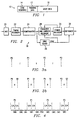
- Figure 1 illustrates such a frame designated generally at 10.
- frame 10 is a quadrature amplitude modulation ("QAM") frame, where it is known in the art that QAM frames encode data in an analog signal which includes one of a different available combination of phases and amplitudes to represent different bit patterns.
- training data 12 is provided within frame 10 to tune an equalizer in the receiving modem.
- frame 10 also includes a synchronization or "sync" sequence 14 placed at the start of frame 10.
- a receiving modem must recognize sync sequence 14 at some point during the receipt of frame 10.
- frame 10 includes user data 16 located after training data 12 and, thus, by locating the position of training data 12, the location of user data 16 also may be determined.
- FIG. 2 illustrates a block diagram of a receiver path in a modem 18.
- the block diagram of modem 18 is a general representation and, thus applies in general to the prior art but also may be modified as described later to form an inventive embodiment.
- Modem 18 receives frame data as an analog signal from a wireline (e.g., a telephone line or a cable, such as a coax cable), and that data is input to an analog-to digital converter (“ADC") 20 where it is converted to a digital form.
- ADC analog-to digital converter
- the digitally converted signal then passes to a timing recovery block 22 that re-times the sampling of the input waveform so that the receive sampling frequency tracks that of the transmitter in frequency.
- the signal passes to a demodulator 24 that removes the data from its modulated form, thereby producing the baseband values of the data.
- the frequency of the baseband value signal output from demodulator 24 is typically at some integer multiple (or other fraction greater than one) of the symbol rate; commonly, therefore, the output of demodulator 24 is at two times the symbol rate.
- the demodulated data passes to both a sync block 26 as well as an equalizer and carrier recovery block 28.
- Sync block 26 locates sync sequence 14 in each frame as detailed below, and when this location occurs sync block 26 asserts a SYNC signal to equalizer and carrier recovery block 28 so that it may synchronize itself to the incoming signal and perform training.
- Equalizer and carrier recovery block 28 outputs the equalized signal to a symbol decision block 30.
- Symbol decision block 30 performs the function of estimating the transmitted data from the output of equalizer and carrier recovery block 28. This is usually performed by finding the nearest point in the signal constellation to each received sample. This result is output to a deframer 32.
- symbol decision block 30 feeds back a signal to equalizer and carrier recover block 28 in order to provide decision-directed tracking of changes in the channel during the data portion of the frame.
- the SYNC signal from sync block 26 is also connected to deframer 32 so that it too may synchronize itself to the incoming signal. Further, deframer 32 performs the function of removing training data 12 and sync sequence 14 from frame 10, thereby leaving only user data 16.
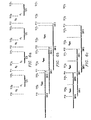
- sync block 26 locates sync sequence 14 in each frame 10 by taking periodic samples, where this approach is now described with the benefit of a general timing illustration in Figures 3a and 3b. Specifically, in Figure 3a, let the points P0 through P3 represent successive ideal sample locations in sync sequence 14, with a common time period T between each location.
- sync block 26 would sample the incoming signal at the exact point in time corresponding to point P0; in the art, this point is sometimes referred to as the center of a so-called eye diagram, with it understood that an actual sample taken at this ideal point is most likely to result in proper synchronization, and any increase in time between this ideal point and the actual sample point correspondingly decreases the synchronization performance (i.e., decreases the chance of successful synchronization). Additionally, given the sampling period T, sync block 26 then also ideally samples at each interval of T thereafter, thereby sampling exactly at the points P1, P2, and P3 illustrated in Figure 3a.
- FIG. 3b again illustrates points P0 through P3, and further illustrates a first scenario where a first actual sample S0 is taken, followed thereafter by additional samples at each period of T thereafter.
- samples are taken at times represented as S0, S1, S2, and S3.
- a technique is used whereby the samples are convolved with a filter correlation sequence that represents a time reversed, complex conjugate of sync sequence 14.
- the convolution determination will peak when sync sequence 14 is aligned with the filter correlation sequence.
- sync sequence 14 is typically formed by selecting from the four highest energy points of the symbol constellation and, indeed, using only the two of those four points that have the greatest spectral distance between them (i.e., -15-j max , +15+j max for QAM).
- the convolution peak may be detected by comparing the convolution result against a threshold, where the threshold is set to a level just below the anticipated maximum peak. Accordingly, when the threshold is exceeded, sync block 26 asserts its SYNC output, thereby informing other blocks in Figure 2 that synchronization has occurred.
- a length of time (or phase shift), indicated in Figure 3b as ⁇ occurs between each ideal sampling point and a corresponding actual sample.
- ⁇ is a length representing a distance between the ideal sampling time and the actual sampling time.
- the peak of the convolution may be less than the anticipated peak.
- the threshold used for comparison is lowered to accommodate the lower corresponding peak.
- the threshold is set too low, then it may be exceeded in some instances when an actual sync sequence has not been detected, which in turn could cause errant assertions of the SYNC output of sync block 26. Quite clearly, these errant assertions of the SYNC output may cause wrongful interpretation of incoming data.
- ⁇ max a maximum value of ⁇ , designated from this point forward as ⁇ max , may be determined empirically under which proper synchronization detection is ensured (or at least expected to meet an accepted confidence level).
- ⁇ max is determined empirically to equal T/4.
- Figure 4 once more illustrates points P0 through P3. Additionally, because ⁇ max equals T/4, then proper operation should occur so long as the sample for each point occurs within a time period no greater than T/4 before or after each such point.
- a sampling window of time having a period from T/4 before the point to T/4 after the point is shown with respect to each of points P0 through P3, labeled for reference as SW0 through SW3, respectively.
- SW0 through SW3 there also are periods of time that do not fall within these sampling widows. Given the preceding definitions, therefore, these periods of time represent instances where, if sampling occurs, proper sync detection may not occur.
- These periods are shown as error windows EW0 through EW3 in Figure 4. Note that each error window occurs beyond both edges of the sample window, that is, because the sample window is by definition centered about the point, then each point will have two corresponding error windows, one before and one after the sample window. Thus, in Figure 4, it is noted that the second instance of error window EW0 following point P0 coincides with a first instance of error window EW1 preceding point P1. A similar observation may be made regarding the remaining sample and error windows.
- the present inventor notes that the prior art may provide various drawbacks. For example, for a given system, if ⁇ max is relatively short, then the error windows EW0 through EW3 are relatively large. Accordingly, the chance of the periodic samples falling within error windows EW0 through EW3 are likewise increased, thereby increasing the likelihood of faulty sync detection, where faults may include both errant indication of synchronization or a total failure to achieve synchronization. Certain attempts may be made to reduce the chances of error by increasing the length of ⁇ max , such as by increasing the number of symbols in sync sequence 14. However, such an approach thereby reduces the bandwidth available for user data and, thus, may be undesirable. Consequently, this as well as other efforts may require greater resources (and cost), or simply may not be acceptable or feasible in various contexts. As a result, there arises a need to address the drawbacks of the prior art, as is achieved by the embodiments described below.
- the modem comprises circuitry for receiving an analog signal from a line and circuitry for converting the analog signal to a digital signal.
- the digital signal comprises a plurality of ideal sample points, each separated in time by a period T, and the plurality of ideal sample points comprises a sync sequence.
- the modem further comprises circuitry for detecting the sync sequence, comprising an integer number S of sampling circuits, where S is two or greater.
- Each of the sampling circuits comprises circuitry for taking a sample corresponding to each of the plurality of ideal sample points at least once per the period T.
- Each of the sampling circuits also comprises circuitry for comparing a plurality of taken samples to a correlation sequence.
- each of the sampling circuits comprises circuitry for outputting a sync detected signal in response to a sufficient match between the plurality of taken samples and the correlation sequence.
- FIG. 5 illustrates a block diagram of an inventive sync block 34.
- sync block 34 may be used in lieu of sync block 26 in Figure 2 to thereby form an inventive embodiment.
- sync block 34 of Figure 5 may be implemented in other wireline modems as well. In any event, any of the improved modems should provide more efficient frame synchronization functionality.
- sync block 34 includes a data input 36 for receiving the demodulated incoming data frames, where those frames are coupled to the input of two different correlators. More particularly, each incoming frame is coupled to a phase 0 correlator 38 and a phase 1 correlator 40. Each phase correlator samples the incoming frame and provides a synchronization ("sync") detected signal to a corresponding input of a post processor 42; for purposes of reference, the sync detected signal provided by phase 0 correlator 38 is identified as SYNC 0 and the sync detected signal provided by phase 1 correlator 40 is identified as SYNC 1 .
- sync synchronization
- Post processor 42 outputs a final sync detected signal, SYNC F , which is usable by various other devices within the modem implementing sync block 34 for purposes of synchronization.
- SYNC F may be used to synchronize sequence and compare circuit 28 and deframer 32 so that they may perform the functions described earlier.
- Sync block 34 also includes a second input 44 for receiving the symbol rate clock, where that rate corresponds to the period T described earlier in connection with Figure 3a.
- Input 44 couples the symbol rate clock to the input of a clock generator 46.
- Clock generator 46 doubles the symbol rate clock, that is, it provides an output clock signal that has a frequency equal to 2/T. This output clock signal is used to clock each of the other illustrated blocks in sync block 34, thereby facilitating a dual sample operation as further detailed in the remaining discussion.
- Figure 6a illustrates ideal sample points P10 through P13 representing successive ideal samples in a sync sequence, again with a symbol period T between each bit.
- Figure 6a also illustrates actual samples S10 0 , S11 0 , S12 0 , and S13 0 taken by phase 0 correlator 38 in relation to ideal sample points P10 through P13, respectively.
- the "0" designation from phase 0 correlator 38 is used as subscript with these samples to illustrate that the samples correspond to phase 0 correlator 38.
- Figure 6a illustrates actual samples S10 1 , S11 1 , S12 1 , and S13 1 taken by phase 1 correlator 40 in relation to ideal sample points P10 through P13, respectively; here, the "1" designation from phase 1 correlator 40 is used as subscript with these actual samples.
- Figure 6a demonstrates that for each ideal sample point both correlators 38 and 40 take an actual sample corresponding thereto.
- phase 0 correlator 38 takes a sample S10 0 at some arbitrary time, and at a time T/2 thereafter phase 1 correlator 10 takes a sample S10 1 . Similar timing observations should thus be apparent for the remaining samples taken and illustrated in Figure 6a. Lastly in this regard, recall that the output of demodulator 24 is commonly at two times the symbol rate and, thus, there is no need to further adjust this signal in order to achieve the T/2 samples by correlators 38 and 40.
- Figure 6a also introduces an important aspect of the distance between alternating samples of correlators 38 and 40 with respect to the ideal sample points P10 through P13. More particularly, in Figure 6a note that the first sample S10 0 by phase 0 correlator 38 occurs at some arbitrary time with respect to ideal sample point P10, and a distance of ⁇ 0 therefore exists between the sample and the corresponding ideal sample point. Because the other samples by phase 0 correlator 38 are later taken at a frequency of 1/T, then in general for subsequent samples they too will be separated by a distance of ⁇ 0 from the corresponding ideal sample point.
- phase 1 correlator 40 samples at a period T/2 thereafter, then a fixed distance relationship is also established between each sample of phase 1 correlator 40 and a corresponding ideal sample point. This fixed distance is shown in Figure 6a as ⁇ 1 .
- ⁇ max may be empirically determined for a system and represents the greatest distance in time which may exist between an ideal sample point and an actual sample point while still permitting acceptable identification of the sync sequence.
- ⁇ max may be empirically determined for a system and represents the greatest distance in time which may exist between an ideal sample point and an actual sample point while still permitting acceptable identification of the sync sequence.
- below are explored several examples to illustrate the potential relationship of ⁇ max to ⁇ 0 and ⁇ 1 , and to thereby demonstrate a benefit of the preferred embodiment.
- Figure 6c also illustrates error windows EW10 through EW12.
- error windows represent the same notion introduced in Figure 4 earlier, that is, if a sample is taken during an error window, it does not provide satisfactory information for detection of the sync sequence. Indeed, in the present example, since ⁇ 1 is greater than ⁇ max , note that the samples S10 1 through S13 1 in Figure 6c fall inside of the error windows. As a result, for the current example the samples taken by phase 1 correlator 40 are not reliable for proper sync sequence detection. However, recall that the samples taken by phase 0 correlator 38 are acceptable for such detection.
- Figure 7 illustrates a different set of ideal sample points P20 through P23 in a sync sequence, along with samples S20 0 , S21 0 , S22 0 , and S23 0 taken by phase 0 correlator 38 and samples S20 1 , S21 1 , S22 1 , and S23 1 taken by phase 1 correlator 40.
- the arbitrary timing of taking the first sample S20 0 causes it to be at a distance ⁇ 0 from P20, where that distance is greater than the distance ⁇ 1 between sample S20 1 and P20.
- ⁇ max is determined to be greater than ⁇ 1 but less than ⁇ 0
- the samples taken by phase 1 correlator 40 provide proper sync sequence detection while the samples taken by phase 0 correlator 38 do not.
- the arbitrary timing of the Figure 7 example demonstrates an instance where the limitation provided by ⁇ max is more likely to exclude the usefulness of the samples taken by phase 0 correlator 38 rather than those taken by phase 1 correlator 40.
- correlators 38 and 40 may provide samples sufficient to detect a sync sequence. Indeed, given the operation as discussed thus far, if ⁇ max is equal to or greater than T/2, then in each instance at least one of the two correlators should take a sample within an acceptable sample window. This may be contrasted with the prior art, where only a value of ⁇ max equal to T would ensure a comparable result. Accordingly, given that ⁇ max may be much smaller than in the prior art while still providing sufficient results, note therefore that such a value of ⁇ max may be achieved with a much shorter sync sequence. This in turn reduces the complexity of each correlator and there is less bandwidth required for overhead, thereby leaving more bandwidth for other data (e.g., user data).
- sync block 34 including two correlators
- an alternative embodiment may be created with an integer S number of correlators where S exceeds two, and where each corresponding correlator takes its sample at a period of T/S apart from any other correlator.
- at least one of the S correlators should provide satisfactory samples so long as the value of ⁇ max is equal to or greater than T/S.
- the two correlators already described may be connected as previously illustrated, but clocked or operated such that each takes more than one sample per period T, thereby providing a total of at least four samples per period T.
- post processor 42 which, recall, in general receives the SYNC 0 and SYNC 1 outputs of the correlators, and in response outputs a final sync detected signal SYNC F .
- the preceding has illustrated that in certain instances, only one of phase 0 correlator 38 or phase 1 correlator 40 will sample within an appropriate sample window. In such an instance, then only that one correlator will assert its SYNC output. However, the preceding has further demonstrated that in other instances, such as where ⁇ max is greater than T/2, both correlators may assert their SYNC outputs.
- Post processor 42 therefore, provides additional functionality to address these various contingent scenarios, as discussed below.
- post processor 42 begins with a step 50 where post processor 42 awaits a sync detected signal pulse from either phase 0 correlator 38 or phase 1 correlator 40. Thus, once either SYNC 0 or SYNC 1 is asserted, method 48 continues from the wait state of step 50 to step 52. Step 52 directs the remaining flow based on which of correlators 38 or 40 asserted its sync detected signal pulse.
- step 54 If the source of the asserted sync detected signal pulse is phase 0 correlator 38, method 48 continues to step 54; conversely, if the source of the asserted sync detected signal pulse is phase 1 correlator 40, method 48 continues to step 56.
- step 54 If the source of the asserted sync detected signal pulse is phase 0 correlator 38, method 48 continues to step 54; conversely, if the source of the asserted sync detected signal pulse is phase 1 correlator 40, method 48 continues to step 56.
- phase 0 correlator 38 i.e., the phase 0 clock
- phase 1 correlator 40 i.e., the phase 1 clock
- each rising edge of a phase clock causes its corresponding correlator to take a sample; thus, consistent with the earlier description, for a single period of the symbol clock, phase 0 correlator 38 takes a sample and at T/2 thereafter phase 1 correlator 40 takes a sample.
- phase 0 correlator 38 is clocked at t 0 , t 2 , t 4 , and so forth.
- Phase 1 correlator 40 is clocked at a time phase shifted by a duration of T/2 after phase 0 correlator 38 is clocked and, thus, for example, is clocked at t 1 , t 3 , t 5 , and so forth.
- step 54 an example of its occurrence is shown as occurring at time t 2 .
- the fourth and fifth rows in Figure 9 illustrate some examples of the SYNC 0 and SYNC 1 outputs, and at time t 2 it is seen that SYNC 0 is asserted.
- step 52 forwards method 48 to step 54, and step 54 asserts SYNC F during the same then current high state of the symbol clock, as shown at t 2 in the sixth row of Figure 9.
- phase 0 correlator 38 is considered a dominant correlator in that its assertion of SYNC 0 always causes an immediate corresponding assertion of SYNC F .
- step 56 having been reached by post processor 42 due to a received assertion of SYNC 1 , post processor 42 determines whether SYNC 0 was asserted for the current period of the symbol clock period (i.e., symbol clock high or low), that is, whether SYNC 0 was asserted at the time T/2 immediately before the current assertion of SYNC 1 . If this is the case, then SYNC F is not asserted and instead method 48 returns to step 50 and awaits the next asserted one of SYNC 0 or SYNC 1 . On the other hand, if SYNC 0 was not asserted at the time T/2 immediately before the current assertion of SYNC 1 , method 40 continues to step 58. Each of these alternative paths is analyzed below.
- step 58 method 48 returns to the wait state of step 50.
- FIG. 10 illustrates a block diagram of an alternative inventive sync block 34'.
- Sync block 34' includes all of the aspects of sync block 34 shown in Figure 5 and, thus, to demonstrate these like items, the same reference numerals are carried forward into Figure 10 and an apostrophe is added thereto.
- sync block 34' includes a second post processor identified generally at 60. More specifically, post processor 60 receives the synchronization signal from post processor 42' and, based on a method detailed below, outputs in various instances its own final sync detected signal, SYNC F ', where SYNC F ' may be connected to various other devices within the modem implementing sync block 34' for purposes of synchronization. To further illustrate this operation and by way of convention, for the Figure 10 embodiment the sync detected signal from post processor 42' is re-named from SYNC F to SYNC 42 to more easily distinguish it from SYNC F ' provided by post processor 60.
- post processor 60 includes a number of counters, with that number selected in a manner discussed later. For the present example, the number equals five and, thus, shown in Figure 11 are counters CTR1 through CTR5.
- Each counter is connected to receive the phase 0 clock signal (i.e., the dominant clock signal) and advances its count, in response to being clocked, from zero to an integer value equal to N-1, where for reasons detailed below N equals the number of clock cycles that should occur between synchronization detection (i.e., from the proper assertion of SYNC F ' to the next proper assertion of SYNC F ').
- post processor 60 includes a pointer PTR that is under the control of a pointer control circuit 62.
- pointer PTR moves in a circular fashion so that it points to a given counter and is then advanced to the next highest counter until it wraps around from counter CTR5 to counter CTR1.
- the values of the counts from each counter are connected as inputs to a counter evaluation circuit 64.
- Counter evaluation circuit 64 operates as detailed later to provide the final sync detected signal SYNC F '.
- post processor 60 The operation of post processor 60 is now discussed.
- the operation of post processor 60 in general is performed preferably in an effort to address a first situation, and may be further expanded in still another embodiment to address a second situation.
- the first situation preferably addressed by post processor 60 is to prevent a spurious assertion of SYNC 42 from reaching the other synchronizing components in the modem.
- the second situation that may be addressed by post processor 60 is to assert SYNC F ' to the other synchronizing components in the modem in the case where SYNC 42 should have been timely asserted but was not (i.e., neither SYNC 0 nor SYNC 1 was timely asserted).
- post processor 60 intercepts any spurious assertion of SYNC 42 in an effort to prevent it from reaching other modem components. More particularly, recall in connection with sync block 34 of Figure 5 that its SYNC F signal as provided by post processor 42 is used to synchronize various other modem circuits. However, it has been determined that various factors, such as noise, may cause an occasional spurious assertion of the sync detected signal from post processor 42 (here re-labeled as SYNC 42 ). Accordingly, in the alternative embodiment of sync block 34' in Figure 10, post processor 60 is added to respond to this event.
- post processor 60 determines that SYNC 42 was properly asserted, then the assertion is immediately translated into a corresponding assertion of SYNC F ' (e.g., by passing SYNC 42 through to SYNC F '). However, if post processor 60 determines that an assertion of SYNC 42 was spurious, then SYNC F ' is not correspondingly asserted. In the preferred embodiment, this aspect is achieved by monitoring the last integer M number of assertions of SYNC 42 and responding as explored in greater detail given the operation of pointer control circuit 62 and counter evaluation circuit 64.
- Method 66 commences with a wait state step 68, where pointer control circuit 62 awaits an assertion of SYNC 42 . During this time and all others, each of the counters advance in response to an assertions (e.g., rising edge) of the phase 0 clock. Once SYNC 42 is asserted, method 66 continues from the wait state of step 68 to step 70.
- step 70 pointer control circuit 62 advances pointer PTR so that it then points to the next higher numbered counter, or given the circular nature described above, if pointer PTR was pointing to counter CTR5 prior to step 70, then step 70 advances pointer PTR so that it then points to counter CTR1. In addition, step 70 clears the count in the newly identified counter.
- step 72 pointer control circuit 62 causes each of the counters to continue to increment for each phase 0 clock where there is no corresponding assertion of SYNC 42 .
- method 66 returns to step 70 so that the next counter is identified by pointer PTR and cleared, followed by a repeat of step 72 so that the next identified counter then counts upward starting from zero and in response to each phase 0 clock where there is no corresponding assertion of SYNC 42 , while the other counters likewise increment in response to the phase 0 clock.
- both counters CTR2 and CTR3 roll over to zero.
- SYNC 42 is asserted, thereby advancing pointer PTR to counter CTR4 and clearing it to zero. This process then continues for each counter so that once pointer PTR has cleared each counter and there have been proper assertions of SYNC 42 every 16 symbol (and phase 0) clocks, then at that point each counter stores a value equal to zero.
- the number of counters here equal to five, defines the amount of past history, that is, the number of most-recently asserted SYNC 42 signals, that are monitored by post processor 60.
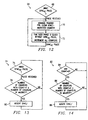
- Method 74 commences with a start step 76, where counter evaluation circuit 64 awaits an assertion of SYNC 42 . Once SYNC 42 is asserted, method 74 continues from the wait state of step 76 to step 78. In step 78, counter evaluation circuit 64 determines whether the number of counters storing a value equal to zero is equal to or greater than the majority of the number of M counters.
- step 78 determines whether at least three counters store a value of zero If so, method 78 continues to step 80, whereas if not, method 78 returns to step 76.
- step 80 having been reached because at least a majority of counters store a value equal to zero, counter evaluation circuit 64 asserts SYNC F ' as corresponding to the asserted SYNC 42 received in step 76. Thereafter, method 74 returns to the wait state of step 76 until the next assertion of SYNC 42 .
- method 74 evaluates the counters to identify either normal operation (i.e., timely assertions of SYNC 42 ) as indicated by the equilibrium of either all or a majority of zero counts described above or, alternatively, to identify a potential spurious assertion of SYNC 42 when a majority of the counters do not reflect the above-described equilibrium. Further, when equilibrium or near-equilibrium is identified, then counter evaluation circuit 64 asserts SYNC F ' in response to a corresponding received assertion of SYNC 42 .
- counter evaluation circuit 64 merely receives the asserted SYNC 42 , but does not assert SYNC F ' so that the other synchronized modem components are not disturbed by this spurious event.
- post processor 60 may respond even if in fact SYNC 42 was not asserted.
- the response by post processor 60 is to insert an assertion of SYNC F ' in the appropriate time slot in an effort to maintain proper synchronization notwithstanding the fact that SYNC 42 was not timely asserted.
- this aspect is also achieved by monitoring the past history of SYNC 42 as represented by the last integer M number of assertions of SYNC 42 , and responding as explored in greater detail with reference to Figure 14.
- Figure 14 illustrates a flowchart of a method 82 which also may be included within the functionality of post processor 60 as introduced above.
- Method 82 commences with a step 84 that waits for the count in any of counters CTR1 through CTR5 to reach zero. When this occurs, method 82 continues from to step 86.
- step 86 counter evaluation circuit 64 determines whether the number of counters storing a value equal to zero is equal to or greater than the majority of the number of M counters. Thus, in the example of post processor 60 in Figure 11, step 86 determines whether at least three counters store a value of zero. If so, method 82 continues to step 88, whereas if not, method 82 returns to step 84.
- step 88 having been reached because at least a majority of counters store a value equal to zero, counter evaluation circuit 64 asserts SYNC F ' regardless of whether SYNC 42 was asserted in the same clock cycle that caused the counter to reach a count of zero from step 84. Thereafter, method 82 returns to the zero detection operation of step 84.
- method 82 evaluates the counters to identify an instance where SYNC 42 should have been asserted but was not, and responds by asserting a final sync signal SYNC F ' because it was expected that SYNC 42 should have been asserted. To further appreciate these operations, below are presented a few numeric examples.
- step 86 determines that the number of counters having a value of zero, which here is all five counters, is equal to or exceeds the number of counters in the majority (i.e., three). Consequently, method 82 continues to step 88 which asserts SYNC F '.
- SYNC F ' is asserted because it was anticipated, based on the past history of SYNC 42 assertions, that SYNC 42 should have been asserted during the current clock which thereby would have caused SYNC F ' to be asserted under method 74 of Figure 13. Accordingly, method 82 effectively inserts a SYNC F ' assertion where one might otherwise not have occurred because SYNC 42 was not asserted (i.e., because neither SYNC 0 nor SYNC 1 were asserted).
- the computer program is stored on a carrier medium in machine or device readable form, for example in solid-state memory or magnetic memory such as disc or tape and the processing device utilises the program or a part thereof to configure it for operation.
- the computer program may be supplied from a remote source embodied in a communications medium such as an electronic signal, radio frequency carrier wave or optical carrier wave.
- a communications medium such as an electronic signal, radio frequency carrier wave or optical carrier wave.
- carrier media are also envisaged as aspects of the present invention.
Landscapes
- Engineering & Computer Science (AREA)
- Computer Networks & Wireless Communication (AREA)
- Signal Processing (AREA)
- Synchronisation In Digital Transmission Systems (AREA)
- Digital Transmission Methods That Use Modulated Carrier Waves (AREA)
Applications Claiming Priority (2)
| Application Number | Priority Date | Filing Date | Title |
|---|---|---|---|
| US13163699P | 1999-04-28 | 1999-04-28 | |
| US131636P | 1999-04-28 |
Publications (2)
| Publication Number | Publication Date |
|---|---|
| EP1049286A2 true EP1049286A2 (de) | 2000-11-02 |
| EP1049286A3 EP1049286A3 (de) | 2004-06-30 |
Family
ID=22450339
Family Applications (1)
| Application Number | Title | Priority Date | Filing Date |
|---|---|---|---|
| EP00303589A Withdrawn EP1049286A3 (de) | 1999-04-28 | 2000-04-28 | Rahmensynchronisierung mit mehrfacher Abtastung |
Country Status (3)
| Country | Link |
|---|---|
| EP (1) | EP1049286A3 (de) |
| JP (1) | JP2000354079A (de) |
| TW (1) | TW472473B (de) |
Family Cites Families (4)
| Publication number | Priority date | Publication date | Assignee | Title |
|---|---|---|---|---|
| GB2206267B (en) * | 1987-06-24 | 1991-09-25 | Plessey Co Plc | Novel correlator for synchronisation detection |
| ES2071554B1 (es) * | 1992-12-30 | 1996-01-16 | Alcatel Standard Electrica | Metodo y dispositivo de recuperacion de datos en sistemas de comunicacion a rafagas. |
| FR2715488B1 (fr) * | 1994-01-21 | 1996-03-22 | Thomson Csf | Procédé et dispositif permettant à un modem de se synchroniser sur un transmetteur de données numériques par voie hertzienne en présence de brouilleurs. |
| US5699389A (en) * | 1995-09-28 | 1997-12-16 | Motorola, Inc. | Oversampling correlator with virtual clock phase for a telecommunications device |
-
2000
- 2000-04-27 JP JP2000126902A patent/JP2000354079A/ja active Pending
- 2000-04-28 TW TW89108135A patent/TW472473B/zh not_active IP Right Cessation
- 2000-04-28 EP EP00303589A patent/EP1049286A3/de not_active Withdrawn
Also Published As
| Publication number | Publication date |
|---|---|
| TW472473B (en) | 2002-01-11 |
| EP1049286A3 (de) | 2004-06-30 |
| JP2000354079A (ja) | 2000-12-19 |
Similar Documents
| Publication | Publication Date | Title |
|---|---|---|
| JP5738406B2 (ja) | フレーム開始デリミタを検出する方法及び装置 | |
| RU2365054C2 (ru) | Система и способ синхронизации кадра и получения начального отсчета времени символа | |
| JP3880358B2 (ja) | Ofdm復調回路及びこれを用いたofdm受信装置 | |
| US20060160545A1 (en) | Methods and apparatus for identifying asset location in communication networks | |
| CN108347397A (zh) | 接收调制信号的接收器和对其进行同步的方法 | |
| KR100914872B1 (ko) | 오버샘플링된 경판정 2 진 스트림으로부터의 심볼 복구 | |
| US6314129B1 (en) | Circuit and method for timing recovery in digital communication receiver | |
| US5495509A (en) | High processing gain acquisition and demodulation apparatus | |
| CN106802424B (zh) | 一种多频卫星导航接收机快速引导跟踪方法及装置 | |
| US6438187B1 (en) | Phase processor for data pattern correlator | |
| US12476852B2 (en) | Phasor-based signal detector | |
| US6765956B1 (en) | Multiple sampling frame synchronization in a wireline modem | |
| EP2947834B1 (de) | Vorrichtung und verfahren zum erfassen und verfolgen von signalen, die durch verschiedene modulationsverfahren moduliert werden | |
| US5949834A (en) | VSB symbol sync recovery system | |
| CN100411333C (zh) | 用于控制从包含至少一个数据分组的数据流中提取数据的方法和设备 | |
| US6396953B1 (en) | Data pattern correlator | |
| EP3208966B1 (de) | Verfahren und system zur verringerung von falscher präambeldetektion in einem kommunikationsempfänger | |
| CN101938347B (zh) | 定时误差提取装置及方法 | |
| CN114157545B (zh) | 一种vdes系统中的16qam解调系统和方法 | |
| JP2002101019A (ja) | 受信機の同期方法および同期装置 | |
| EP1049286A2 (de) | Rahmensynchronisierung mit mehrfacher Abtastung | |
| CN102223345B (zh) | 时隙同步与符号同步的方法 | |
| CN111490955B (zh) | 一种在大频偏下实现同步头搜索的方法及装置 | |
| GB2402030A (en) | Timing recovery loop with non-integer length | |
| JP5237665B2 (ja) | 同期確立方法、直交周波数分割多重変調方法、通信装置 |
Legal Events
| Date | Code | Title | Description |
|---|---|---|---|
| PUAI | Public reference made under article 153(3) epc to a published international application that has entered the european phase |
Free format text: ORIGINAL CODE: 0009012 |
|
| AK | Designated contracting states |
Kind code of ref document: A2 Designated state(s): AT BE CH CY DE DK ES FI FR GB GR IE IT LI LU MC NL PT SE |
|
| AX | Request for extension of the european patent |
Free format text: AL;LT;LV;MK;RO;SI |
|
| PUAL | Search report despatched |
Free format text: ORIGINAL CODE: 0009013 |
|
| AK | Designated contracting states |
Kind code of ref document: A3 Designated state(s): AT BE CH CY DE DK ES FI FR GB GR IE IT LI LU MC NL PT SE |
|
| AX | Request for extension of the european patent |
Extension state: AL LT LV MK RO SI |
|
| AKX | Designation fees paid |
Designated state(s): DE |
|
| STAA | Information on the status of an ep patent application or granted ep patent |
Free format text: STATUS: THE APPLICATION IS DEEMED TO BE WITHDRAWN |
|
| 18D | Application deemed to be withdrawn |
Effective date: 20050202 |