EP1049160A1 - New contact shape for giga scale borderless contacts and method for making the same - Google Patents
New contact shape for giga scale borderless contacts and method for making the same Download PDFInfo
- Publication number
- EP1049160A1 EP1049160A1 EP00108501A EP00108501A EP1049160A1 EP 1049160 A1 EP1049160 A1 EP 1049160A1 EP 00108501 A EP00108501 A EP 00108501A EP 00108501 A EP00108501 A EP 00108501A EP 1049160 A1 EP1049160 A1 EP 1049160A1
- Authority
- EP
- European Patent Office
- Prior art keywords
- contact
- substrate
- semiconductor device
- active area
- borderless
- Prior art date
- Legal status (The legal status is an assumption and is not a legal conclusion. Google has not performed a legal analysis and makes no representation as to the accuracy of the status listed.)
- Withdrawn
Links
Images


Classifications
-
- H—ELECTRICITY
- H10—SEMICONDUCTOR DEVICES; ELECTRIC SOLID-STATE DEVICES NOT OTHERWISE PROVIDED FOR
- H10B—ELECTRONIC MEMORY DEVICES
- H10B12/00—Dynamic random access memory [DRAM] devices
- H10B12/30—DRAM devices comprising one-transistor - one-capacitor [1T-1C] memory cells
- H10B12/48—Data lines or contacts therefor
- H10B12/485—Bit line contacts
-
- H—ELECTRICITY
- H10—SEMICONDUCTOR DEVICES; ELECTRIC SOLID-STATE DEVICES NOT OTHERWISE PROVIDED FOR
- H10D—INORGANIC ELECTRIC SEMICONDUCTOR DEVICES
- H10D99/00—Subject matter not provided for in other groups of this subclass
-
- H—ELECTRICITY
- H10—SEMICONDUCTOR DEVICES; ELECTRIC SOLID-STATE DEVICES NOT OTHERWISE PROVIDED FOR
- H10B—ELECTRONIC MEMORY DEVICES
- H10B12/00—Dynamic random access memory [DRAM] devices
- H10B12/30—DRAM devices comprising one-transistor - one-capacitor [1T-1C] memory cells
- H10B12/37—DRAM devices comprising one-transistor - one-capacitor [1T-1C] memory cells the capacitor being at least partially in a trench in the substrate
Definitions
- This invention relates to the fabrication of integrated circuit devices and, more particularly, to a borderless contact structure and its method of manufacture.
- borders were introduced to compensate for the inability to precisely align a contact mask with the device areas in order to open contact holes through an insulating layer. The borders ensure that the contact openings will never extend beyond the structure or the regions with which contact is made. However, these borders reduce the available space on the substrate and limit the number of cells or integrated circuits. Thus, borderless contact structures have been employed in order to permit more cells per chip.
- Borderless contacts do not require a border around a contact.
- a borderless contact is a contact which overlies and exposes the active and isolation regions, and gates of the semiconductor device, usually for the purpose of making contact to a diffusion region formed in the substrate.
- the contacts are always borderless to the gates, but may be only partially borderless to the active regions under misalignment conditions.
- the contacts are typically formed in a manner which avoids shorting of the diffused junctions to adjacent structures without being limited by lithographic overlay tolerances.
- junction capacitance can be reduced by decreasing the area of the source and drain regions.
- Junction resistance can be reduced by better alignment of the contacts so that they extend close to the channel region.
- the process window for lithographic and etch techniques is critical to the manufacture of integrated circuits. Fabrication issues involving overlay requirements, areal image improvements, reduced etch stop, reduced aspect ratio, improved contact resistance, and increased process windowing, remain technical challenges for a gigabit groundrule process.
- a further object of the invention is to provide a borderless contact array for increasing the lithographic process window.
- a semiconductor device comprising: a substrate; at least one conductor and at least one isolation region on the substrate; at least one active area overlapping the at least one conductor; and a borderless contact structure contacting the active area, the borderless contact structure comprising: a lower portion in contact with the active area, the lower portion defined by a spacing between the at least one conductor and by the at least one isolation region; and an upper portion disposed over the conductors having length and width dimensions, the length to width dimension having a greater ratio than about one wherein the length is in a direction substantially perpendicular to the at least one conductors.
- the present invention is directed to a semiconductor device comprising: a substrate; an active area and a bit line conductor having a direction of elongation, on the substrate; at least two gate structures; and a borderless contact structure contacting the active area, the borderless contact having a lower section where contact is made with the active area and an upper section parallel with the active area, wherein the upper section has substantially orthogonal major and minor axes, the major axis being substantially aligned with the direction of elongation of the bit line conductor and the major to minor axes has a ratio greater than about one.
- the present invention is directed to, in a third aspect, a method of forming a contact in a semiconductor device having a plurality of gate structures and bitlines with minimal ground rule dimensions disposed on the semiconductor substrate comprising the steps of: forming spacers on vertical surfaces of the plurality of gate structures; depositing a conformal layer of dielectric over the substrate and the plurality of gate structures; aligning and etching a plurality of trenches into the dielectric exposing the substrate between the plurality of gate structures; and forming a contact by depositing a conductive material into the trench, the contact having a lower portion in contact with the substrate, and an upper portion in contact with the dielectric, the upper portion having a first side and a second side, the first side being greater than the second side in a direction parallel to the bitlines.
- the present invention is directed to a method of fabricating a semiconductor device having consistent maximum allowable contact areas comprising the steps of: providing a substrate having a plurality of gates and bitlines; the gates forming at least two word lines; forming spacers on vertical walls of the at least two word lines; depositing a conformal layer of dielectric over the substrate; etching a contact area in the dielectric in alignment with the at least two word lines such that a portion of the substrate between the at least two word lines is exposed, the contact area having a lower portion, the lower portion in contact with the substrate, and an upper portion, the upper portion in contact with a top surface of the at least two word lines and the dielectric and having a width and a length, the length being greater than the width by a factor of greater than one in a direction parallel to the bitlines; depositing a conductive material into the contact area to form a contact having lower and upper sections.
- the present invention is directed to a semiconductor device comprising: a substrate; at least one conductor, at least one bitline, and at least one isolation region on the substrate; at least one active area overlapping the at least one conductor; and a self-aligned borderless contact structure contacting the active area, the borderless contact structure comprising: a lower portion in contact with the active area, the lower portion defined by a spacing between the at least one conductor and by the at least one isolation region; and an upper portion disposed over the conductors having length and width dimensions, the length to width dimension having a greater ratio than about one wherein the length is in a direction substantially parallel to the at least one bitline.
- FIG. 1A depicts a conventional contact array having a square borderless contact 10 with contact area 12.
- the contact connects diffusion regions (drain and source regions of a field effect transistor) to metal bitlines 16.
- the footprint of the square contact has length (l) and width (w) dimensions typically on the order of 0.225 micrometers (for a 0.175 m ground rule). This poses lithographic and alignment problems commonly associated with these small dimensions.
- a more or less perpendicular configuration of active area and wordline as well as wordline to the first metal line is assumed.
- Fig. 1B depicts the rectangular borderless contact structure 11 of the instant invention.
- One dimension (l) of the contact structure has been increased.
- this dimension is increased to approximately 0.350 ⁇ m (for a 0.175 ⁇ m ground rule).
- the contact is widened either in the direction perpendicular to the wordline 14 or parallel to the bitline 16. This approach was not attempted in the prior art due to the shorting of the bitlines by the increased contact size.
- a simple widening of the contact size i.e., a larger square contact, does not suffice as a result of possible shorting.
- the shrinkage of the overlay specification with shrinking design rule also remains a challenge for current lithographic tools.
- the overlay specification is approximately three to four tenths of the design rule.
- Meeting this overlay specification is extremely critical to contact resistance and etch.
- an increase in the contact size in the bitline direction is adopted. This ensures that the whole available active area between the wordline is utilized, and that the contact is bordered by gates on both sides.
- etching is the process that is preferably used to ensure the contact is truly bordered by the gates on two opposite sides of the contact, and by the isolation regions on the other adjacent sides.
- the gates are typically isolated with a silicon nitride cap and spacer.
- the RIE etch must progress down more in the middle of the gates than on each gate edge.
- An etch that is at the border or edge of the gate, between spacer and gate, or at the edge of the spacer, runs a higher risk of wordline-bitline shorting, i.e., there is reduced corner selectivity.
- the etching process results in an etched column that is on top of or beside the spacer, a higher etch rate results, requiring more spacer removal and higher stud to wordline capacity.
- the needed overlap of contact and wordline can be achieved with a wider contact, since the overlap of contact and gates is optimized and not reduced with shrinking groundrule and contact size.
- the contact fill will be greatly facilitated.
- the contact resistance between the metal line and the stud is considerably reduced due to the gain in contact size between the metal line and the stud. A more stable contact resistance is realized due to the inherent 100% usage of the available active area.
- Fig. 2 depicts the cross-section of a semiconductor device 20 having a silicon substrate 22 with gate structures 24, silicon nitride spacers 23, and deep trench capacitors 26.
- the deep trench capacitors are isolated by oxide collars 27.
- the maximum available contact area 12 is shown between two silicon nitride gate structures (wordlines). Two gate structures are shown over shallow trench isolation barriers 28.
- An oxide dielectric 30 is then deposited on the semiconductor device 20, as shown in Fig. 3.
- Figure 4A shows this oxide dielectric layer 30 having a photoresist applied 32, and subjected to a lithographic and etching process. The removal of the dielectric layer forms an etched column 34 that is desirably centered between two gate structures 24, thus exposing the maximum allowable contact area 12.
- Fig. 4B depicts a typical misalignment of the etch column in this process.
- a metal line 42 and contact 44 is deposited by the damascene process as shown in Fig. 7.
- this deposited metal structure is a tungsten material.
- the entire contact area 12 is now capable of being attached to contact 44 in a misalignment configuration.
- the rectangular borderless contact is defined above for an xide isolation structure with etching oxide selective to nitrides.
- a complementary etch process or other selective etch process may be used, i.e., etching nitrides instead of oxides.
- a rectangular borderless contact structure capable of maintaining consistent maximum allowable contact area during process misalignments is introduced, along with the method for making the structure.
Landscapes
- Internal Circuitry In Semiconductor Integrated Circuit Devices (AREA)
- Semiconductor Memories (AREA)
- Electrodes Of Semiconductors (AREA)
Abstract
Process misalignments are mitigated, and contact resistance is lowered and kept uniform. The maximum allowable contact area is available even under misalignment configurations.
Description
- This invention relates to the fabrication of integrated circuit devices and, more particularly, to a borderless contact structure and its method of manufacture.
- The formation of electrical contacts where lithographic overlay tolerances must be allowed have caused shorting between the contacts and adjacent structures. Borders were introduced to compensate for the inability to precisely align a contact mask with the device areas in order to open contact holes through an insulating layer. The borders ensure that the contact openings will never extend beyond the structure or the regions with which contact is made. However, these borders reduce the available space on the substrate and limit the number of cells or integrated circuits. Thus, borderless contact structures have been employed in order to permit more cells per chip.
- Borderless contacts do not require a border around a contact. A borderless contact is a contact which overlies and exposes the active and isolation regions, and gates of the semiconductor device, usually for the purpose of making contact to a diffusion region formed in the substrate. The contacts are always borderless to the gates, but may be only partially borderless to the active regions under misalignment conditions. The contacts are typically formed in a manner which avoids shorting of the diffused junctions to adjacent structures without being limited by lithographic overlay tolerances.
- Current state of the art has concentrated on methods of fabricating borderless contacts such that only the desired regions are exposed and other regions remained covered or protected. In U.S. Patent No. 4,944,682 issued to Cronin, et al., on 31 July 1990, entitled, "METHOD OF FORMING BORDERLESS CONTACTS," semiconductor device components are formed wherein there are at least two exposed conducting regions having passivating material overlying these regions. An electrical conducting material then covers the region, and all are subjected to a given etchant. Only those regions having the passivating material not covered with the etch resistant material are removed.
- Previous methods of fabricating microelectronic devices have emphasized a reduction in parasitic capacitance and resistance through different contact formations between the junctions of semiconductor transistors. Junction capacitance can be reduced by decreasing the area of the source and drain regions. Junction resistance can be reduced by better alignment of the contacts so that they extend close to the channel region.
- For a borderless array contact of a gigabit ground rule device, the process window for lithographic and etch techniques is critical to the manufacture of integrated circuits. Fabrication issues involving overlay requirements, areal image improvements, reduced etch stop, reduced aspect ratio, improved contact resistance, and increased process windowing, remain technical challenges for a gigabit groundrule process.
- Bearing in mind the problems and deficiencies of the prior art, it is therefore an object of the present invention to provide a semiconductor device having a more consistent maximum allowable contact area adapted to shrinking ground rule dimensions with a more stable contact resistance.
- It is another object of the present invention to provide a contact shape for improved giga scale borderless contacts.
- A further object of the invention is to provide a borderless contact array for increasing the lithographic process window.
- It is yet another object of the present invention to provide a borderless contact that can compensate for process variations causing misalignment.
- Still other advantages of the invention will in part be obvious and will in part be apparent from the specification.
- The above and other objects and advantages, which will be apparent to one of skill in the art, are achieved in the present invention which is directed to, in a first aspect, a semiconductor device comprising: a substrate; at least one conductor and at least one isolation region on the substrate; at least one active area overlapping the at least one conductor; and a borderless contact structure contacting the active area, the borderless contact structure comprising: a lower portion in contact with the active area, the lower portion defined by a spacing between the at least one conductor and by the at least one isolation region; and an upper portion disposed over the conductors having length and width dimensions, the length to width dimension having a greater ratio than about one wherein the length is in a direction substantially perpendicular to the at least one conductors.
- In a second aspect, the present invention is directed to a semiconductor device comprising: a substrate; an active area and a bit line conductor having a direction of elongation, on the substrate; at least two gate structures; and a borderless contact structure contacting the active area, the borderless contact having a lower section where contact is made with the active area and an upper section parallel with the active area, wherein the upper section has substantially orthogonal major and minor axes, the major axis being substantially aligned with the direction of elongation of the bit line conductor and the major to minor axes has a ratio greater than about one.
- The present invention is directed to, in a third aspect, a method of forming a contact in a semiconductor device having a plurality of gate structures and bitlines with minimal ground rule dimensions disposed on the semiconductor substrate comprising the steps of: forming spacers on vertical surfaces of the plurality of gate structures; depositing a conformal layer of dielectric over the substrate and the plurality of gate structures; aligning and etching a plurality of trenches into the dielectric exposing the substrate between the plurality of gate structures; and forming a contact by depositing a conductive material into the trench, the contact having a lower portion in contact with the substrate, and an upper portion in contact with the dielectric, the upper portion having a first side and a second side, the first side being greater than the second side in a direction parallel to the bitlines.
- In a fourth aspect, the present invention is directed to a method of fabricating a semiconductor device having consistent maximum allowable contact areas comprising the steps of: providing a substrate having a plurality of gates and bitlines; the gates forming at least two word lines; forming spacers on vertical walls of the at least two word lines; depositing a conformal layer of dielectric over the substrate; etching a contact area in the dielectric in alignment with the at least two word lines such that a portion of the substrate between the at least two word lines is exposed, the contact area having a lower portion, the lower portion in contact with the substrate, and an upper portion, the upper portion in contact with a top surface of the at least two word lines and the dielectric and having a width and a length, the length being greater than the width by a factor of greater than one in a direction parallel to the bitlines; depositing a conductive material into the contact area to form a contact having lower and upper sections.
- In a fifth aspect, the present invention is directed to a semiconductor device comprising: a substrate; at least one conductor, at least one bitline, and at least one isolation region on the substrate; at least one active area overlapping the at least one conductor; and a self-aligned borderless contact structure contacting the active area, the borderless contact structure comprising: a lower portion in contact with the active area, the lower portion defined by a spacing between the at least one conductor and by the at least one isolation region; and an upper portion disposed over the conductors having length and width dimensions, the length to width dimension having a greater ratio than about one wherein the length is in a direction substantially parallel to the at least one bitline.
- The features of the invention believed to be novel and the elements characteristic of the invention are set forth with particularity in the appended claims. The figures are for illustration purposes only and are not drawn to scale. The invention itself, however, both as to organization and method of operation, may best be understood by reference to the detailed description which follows taken in conjunction with the accompanying drawings in which:
- Fig. 1A is a top view of a semiconductor device having a conventional contact array.
- Fig. 1B is a top view of a semiconductor device having a rectangular borderless contact structure.
- Fig. 2 depicts the cross-section of a semiconductor device with gate structures and deep trench capacitors.
- Fig. 3 depicts the cross-section of a semiconductor device of Fig. 2 with an oxide dielectric deposition on the surface.
- Fig. 4A depicts the cross-section of a semiconductor device of Fig. 3 with a photoresist applied and an etched column for a properly aligned contact to gate.
- Fig. 4B is a cross-section of a semiconductor device having an etched column that is misaligned between two gate structures.
- Fig. 5 is a cross-section of a semiconductor device having the misalignment shown in Fig. 4B, but with a rectangular borderless contact allowing for maximum contact area.
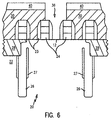
- Fig. 6 is a cross-section of the semiconductor device of Fig. 5 having an etched column for a rectangular contact that is properly aligned between two gate structures.
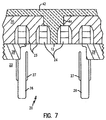
- Fig. 7 is a cross-section of the semiconductor device of Fig. 6 having a metal line deposited in an etched trench and an etched column.
-
- In describing the preferred embodiment of the present invention, reference will be made herein to Figs. 1-7 of the drawings in which like numerals refer to like features of the invention. Features of the invention are not necessarily shown to scale in the drawings.
- A widening of the contact perpendicular to the wordline direction (parallel to the MO metal line) results in improvements in all process steps. This is accomplished by making an otherwise square borderless contact structure into a rectangular structure. Figure 1A depicts a conventional contact array having a square
borderless contact 10 withcontact area 12. The contact connects diffusion regions (drain and source regions of a field effect transistor) tometal bitlines 16. The footprint of the square contact has length (l) and width (w) dimensions typically on the order of 0.225 micrometers (for a 0.175 m ground rule). This poses lithographic and alignment problems commonly associated with these small dimensions. In the placement of the borderless contact structure, a more or less perpendicular configuration of active area and wordline as well as wordline to the first metal line is assumed. Fig. 1B depicts the rectangularborderless contact structure 11 of the instant invention. One dimension (l) of the contact structure has been increased. Preferably, this dimension is increased to approximately 0.350 µm (for a 0.175 µm ground rule). The contact is widened either in the direction perpendicular to thewordline 14 or parallel to thebitline 16. This approach was not attempted in the prior art due to the shorting of the bitlines by the increased contact size. Significantly, a simple widening of the contact size, i.e., a larger square contact, does not suffice as a result of possible shorting. - Actual integration schemes for current borderless contacts are then employed. The dimension changes can be easily implemented by changing one mask. These changes have no impact on bitline-to-bitline shorts yield. For a lithography process, the wider contact area and larger size of the borderless contact in one dimension results in a better areal image, and importantly, in a wider lithographic process window. The new contact area (for a 0.175 µm ground rule) is on the order of 0.0788 µm2 (0.350 µm x 0.225 µm), whereas the prior art contacts, with square contact shapes, have a footprint area of approximately 0.0506 µm2 (0.225 µm x 0.225 µm). Thus, making a borderless contact with a major and minor axis, such that the major to minor axis ratio is greater than one, i.e., a contact rectangular or oval in shape, results in approximately a 56% increase in contact area under normal process variations.
- The shrinkage of the overlay specification with shrinking design rule also remains a challenge for current lithographic tools. Typically the overlay specification is approximately three to four tenths of the design rule. Meeting this overlay specification is extremely critical to contact resistance and etch. In order to meet the overlay specification, especially in the direction perpendicular to the gates or wordline or parallel to the bitlines, an increase in the contact size in the bitline direction is adopted. This ensures that the whole available active area between the wordline is utilized, and that the contact is bordered by gates on both sides.
- For borderless contacts, selective etching is the process that is preferably used to ensure the contact is truly bordered by the gates on two opposite sides of the contact, and by the isolation regions on the other adjacent sides. The gates are typically isolated with a silicon nitride cap and spacer. Important to this process, the RIE etch must progress down more in the middle of the gates than on each gate edge. An etch that is at the border or edge of the gate, between spacer and gate, or at the edge of the spacer, runs a higher risk of wordline-bitline shorting, i.e., there is reduced corner selectivity. If the etching process results in an etched column that is on top of or beside the spacer, a higher etch rate results, requiring more spacer removal and higher stud to wordline capacity. Thus, the needed overlap of contact and wordline can be achieved with a wider contact, since the overlap of contact and gates is optimized and not reduced with shrinking groundrule and contact size. Similarly, with an increased contact size and reduced aspect ratio, the contact fill will be greatly facilitated. Also, the contact resistance between the metal line and the stud is considerably reduced due to the gain in contact size between the metal line and the stud. A more stable contact resistance is realized due to the inherent 100% usage of the available active area.
- Fig. 2 depicts the cross-section of a
semiconductor device 20 having asilicon substrate 22 withgate structures 24,silicon nitride spacers 23, anddeep trench capacitors 26. The deep trench capacitors are isolated byoxide collars 27. The maximumavailable contact area 12 is shown between two silicon nitride gate structures (wordlines). Two gate structures are shown over shallowtrench isolation barriers 28. Anoxide dielectric 30 is then deposited on thesemiconductor device 20, as shown in Fig. 3. Figure 4A shows thisoxide dielectric layer 30 having a photoresist applied 32, and subjected to a lithographic and etching process. The removal of the dielectric layer forms an etchedcolumn 34 that is desirably centered between twogate structures 24, thus exposing the maximumallowable contact area 12. However, in many instances, due to the small contact tolerances and inherent process limitations, misalignment of the etch column remains a problem in the art. This makes centering of the etched column very difficult to achieve under the current process limitations. Fig. 4B depicts a typical misalignment of the etch column in this process. - As shown in Fig. 5, under a misalignment configuration, a
wider etch column 36 will still expose the maximumallowable contact area 12 for the borderless contact. Thus, having a rectangular borderless contact ensures maximum contact area exposure during processing, even under misalignment conditions. - Again, adapting the prior art application to larger square borderless contact structures is not an acceptable solution because of the bitline and wordline shorting that would occur.
- When this process is implemented for rectangular borderless contacts (where the contact is wider in one dimension), it is more accommodating of structure tolerances and process deviations. As indicated in Fig. 6, a
wider etch column 36 is used to clear the way for the contact deposition layer. This wider column compensates for tight tolerance misalignments that are prevalent in the prior art. Additionally, atrench 40 is created for metal line deposition. - Once the photoresist for the bitline has been removed, a
metal line 42 andcontact 44 is deposited by the damascene process as shown in Fig. 7. Preferably, this deposited metal structure is a tungsten material. Importantly, theentire contact area 12 is now capable of being attached to contact 44 in a misalignment configuration. - The rectangular borderless contact is defined above for an xide isolation structure with etching oxide selective to nitrides. However, a complementary etch process or other selective etch process may be used, i.e., etching nitrides instead of oxides.
- A rectangular borderless contact structure capable of maintaining consistent maximum allowable contact area during process misalignments is introduced, along with the method for making the structure.
- While the present invention has been particularly described, in conjunction with a specific preferred embodiment, it is evident that many alternatives, modifications and variations will be apparent to those skilled in the art in light of the foregoing description. It is therefore contemplated that the appended claims will embrace any such alternatives, modifications and variations as falling within the true scope and spirit of the present invention.
Claims (22)
- A semiconductor device comprising:a substrate;at least one conductor and at least one isolation region on said substrate;at least one active area overlapping said at least one conductor; anda borderless contact structure contacting said active area, said borderless contact structure comprising:(i) a lower portion in contact with said active area, said lower portion defined by a spacing between said at least one conductor and by said at least one isolation region; and(ii an upper portion disposed over said conductors having length and width dimensions, the length to width dimension having a greater ratio than about one wherein the length is in a direction substantially perpendicular to said at least one conductor.
- The semiconductor device of claim 1 further including a conductive line in electrical connection with said contact structure.
- The semiconductor device of claim 1 wherein said at least two conductors comprise word lines.
- The semiconductor device of claim 3 wherein said word lines comprise gate structures.
- The semiconductor device of claim 1 wherein said at least two conductors comprise bit lines.
- The semiconductor device of claim 1 wherein said contact structure comprises tungsten.
- The semiconductor device of claim 1 wherein said contact structure comprises polysilicon.
- The semiconductor device of claim 1 further including dielectric spacers within said spacing between said at least two conductors.
- The semiconductor device of claim 8 wherein said spacers comprise silicon nitride.
- The semiconductor device of claim 1 wherein said contact structure electrically connects a substrate of said device to a metal line.
- A semiconductor device comprising:a substrate;an active area and a bit line conductor having a direction of elongation, on said substrate;at least two gate structures; anda borderless contact structure contacting said active area, said borderless contact having a lower section where contact is made with said active area and an upper section parallel with said active area, wherein said upper section has substantially orthogonal major and minor axes, said major axis being substantially aligned with the direction of elongation of said bit line conductor and said major to minor axes has a ratio greater than about one.
- The semiconductor device of claim 11 wherein said upper portion of said contact structure may be misaligned along said major axis between said at least two device structures while said lower portion is in contact with an entire surface of said active area.
- A method of forming a contact in a semiconductor device having a plurality of gate structures and bitlines with minimal ground rule dimensions disposed on said semiconductor substrate comprising the steps of:(a) forming spacers on vertical surfaces of the plurality of gate structures;(b) depositing a conformal layer of dielectric over the substrate and the plurality of gate structures;(c) aligning and etching a plurality of trenches into said dielectric exposing the substrate between the plurality of gate structures; and(d) forming a contact by depositing a conductive material into said trench, said contact having a lower portion in contact with the substrate, and an upper portion in contact with said dielectric, said upper portion having a first side and a second side, said first side being greater than said second side in a direction parallel to said bitlines.
- The method of claim 13 further including the step of depositing a metal liner into said trench prior to step (d).
- The method of claim 13 wherein a dimension of said first side to a dimension of said second side has a ratio greater than about one.
- A method of fabricating a semiconductor device having consistent maximum allowable contact areas comprising the steps of:(a) providing a substrate having a plurality of gates and bitlines; said gates forming at least two word lines;(b) forming spacers on vertical walls of said at least two word lines;(c) depositing a conformal layer of dielectric over said substrate;(d) etching a contact area in said dielectric in alignment with said at least two word lines such that a portion of said substrate between said at least two word lines is exposed, said contact area having a lower portion, the lower portion in contact with said substrate, and an upper portion, the upper portion in contact with a top surface of said at least two word lines and said dielectric and having a width and a length, said length being greater than said width by a factor of greater than one in a direction parallel to said bitlines;(e) depositing a conductive material into said contact area to form a contact having lower and upper sections.
- The method of claim 16 wherein the upper section of said contact can substantially correct misalignment of said contact area in a direction perpendicular to said word lines during step (d) such that an entire area of said substrate between said at least two word lines forms the lower section of said contact.
- The method of claim 16 wherein in step (b) said spacers comprise silicon nitride.
- The method of claim 16 wherein step (e) further includes the step of depositing a liner metal into said contact area followed by depositing tungsten into said contact area to form said contact.
- The method of claim 16 wherein step (e) further includes the step of depositing a liner metal into said contact area followed by polysilicon into said contact area to form said contact.
- The method of claim 16 wherein in step (c) said dielectric comprises silicon oxide.
- A semiconductor device comprising:a substrate;at least one conductor, at least one bitline, and at least one isolation region on said substrate;at least one active area between said at least one conductor; anda self-aligned borderless contact structure contacting said active area, said borderless contact structure comprising:(i) a lower portion in contact with said active area, said lower portion defined by a spacing between said at least one conductor and by said at least one isolation region; and(ii) an upper portion disposed over said conductors having length and width dimensions, the length to width dimension having a greater ratio than about one wherein the length is in a direction substantially parallel to said at least one bitline.
Applications Claiming Priority (2)
| Application Number | Priority Date | Filing Date | Title |
|---|---|---|---|
| US299134 | 1994-09-02 | ||
| US29913499A | 1999-04-26 | 1999-04-26 |
Publications (1)
| Publication Number | Publication Date |
|---|---|
| EP1049160A1 true EP1049160A1 (en) | 2000-11-02 |
Family
ID=23153447
Family Applications (1)
| Application Number | Title | Priority Date | Filing Date |
|---|---|---|---|
| EP00108501A Withdrawn EP1049160A1 (en) | 1999-04-26 | 2000-04-19 | New contact shape for giga scale borderless contacts and method for making the same |
Country Status (6)
| Country | Link |
|---|---|
| EP (1) | EP1049160A1 (en) |
| JP (1) | JP2000315782A (en) |
| KR (1) | KR100363376B1 (en) |
| CN (1) | CN1280389A (en) |
| SG (1) | SG94723A1 (en) |
| TW (1) | TW451407B (en) |
Cited By (2)
| Publication number | Priority date | Publication date | Assignee | Title |
|---|---|---|---|---|
| EP1424733A2 (en) * | 2002-11-28 | 2004-06-02 | Infineon Technologies AG | Method and device for arranging contacts of elements on an integrated circuit, computer readable memory device, and program element |
| US8533639B2 (en) * | 2011-09-15 | 2013-09-10 | Taiwan Semiconductor Manufacturing Company, Ltd. | Optical proximity correction for active region design layout |
Families Citing this family (2)
| Publication number | Priority date | Publication date | Assignee | Title |
|---|---|---|---|---|
| KR100796644B1 (en) | 2007-02-22 | 2008-01-22 | 삼성전자주식회사 | DRAM device and forming method thereof |
| KR102057067B1 (en) * | 2013-01-29 | 2019-12-18 | 삼성전자주식회사 | Metal interconnect structure of a semiconductor device and method for forming the same |
Citations (3)
| Publication number | Priority date | Publication date | Assignee | Title |
|---|---|---|---|---|
| JPS6053085A (en) * | 1983-09-02 | 1985-03-26 | Hitachi Ltd | Junction type field-effect transistor |
| JPH01146356A (en) * | 1987-12-03 | 1989-06-08 | Matsushita Electron Corp | Semiconductor memory device |
| US4944682A (en) * | 1988-10-07 | 1990-07-31 | International Business Machines Corporation | Method of forming borderless contacts |
Family Cites Families (3)
| Publication number | Priority date | Publication date | Assignee | Title |
|---|---|---|---|---|
| US6057604A (en) * | 1993-12-17 | 2000-05-02 | Stmicroelectronics, Inc. | Integrated circuit contact structure having gate electrode protection for self-aligned contacts with zero enclosure |
| JPH08203998A (en) * | 1995-01-20 | 1996-08-09 | Sony Corp | Method of forming multilayer wiring |
| US5671175A (en) * | 1996-06-26 | 1997-09-23 | Texas Instruments Incorporated | Capacitor over bitline DRAM cell |
-
2000
- 2000-04-10 SG SG200002013A patent/SG94723A1/en unknown
- 2000-04-13 CN CN00106570A patent/CN1280389A/en active Pending
- 2000-04-17 KR KR1020000020155A patent/KR100363376B1/en not_active Expired - Fee Related
- 2000-04-19 EP EP00108501A patent/EP1049160A1/en not_active Withdrawn
- 2000-04-25 JP JP2000123911A patent/JP2000315782A/en active Pending
- 2000-06-12 TW TW089107576A patent/TW451407B/en not_active IP Right Cessation
Patent Citations (3)
| Publication number | Priority date | Publication date | Assignee | Title |
|---|---|---|---|---|
| JPS6053085A (en) * | 1983-09-02 | 1985-03-26 | Hitachi Ltd | Junction type field-effect transistor |
| JPH01146356A (en) * | 1987-12-03 | 1989-06-08 | Matsushita Electron Corp | Semiconductor memory device |
| US4944682A (en) * | 1988-10-07 | 1990-07-31 | International Business Machines Corporation | Method of forming borderless contacts |
Non-Patent Citations (4)
| Title |
|---|
| KAWAZU Y ET AL: "NOVEL ELFIN (EMBEDDED-METAL-LAYER PROCESS FOR FULLY INTEGRATED NOR)CELL FOR 16/ 64 MBIT FLASH EEPROM", ELECTRONICS LETTERS,GB,IEE STEVENAGE, vol. 30, no. 15, 21 July 1994 (1994-07-21), pages 1209 - 1210, XP000461660, ISSN: 0013-5194 * |
| KOGA H ET AL: "TWO-DIMENSIONAL BORDERLESS CONTACT PAD TECHNOLOGY FOR A 0.135 MUM2 4-GIGABIT DRAM CELL", INTERNATIONAL ELECTRON DEVICES MEETING,US,NEW YORK, NY: IEEE, 7 December 1997 (1997-12-07), pages 25 - 28, XP000855738, ISBN: 0-7803-4101-5 * |
| PATENT ABSTRACTS OF JAPAN vol. 009, no. 181 (E - 331) 26 July 1985 (1985-07-26) * |
| PATENT ABSTRACTS OF JAPAN vol. 013, no. 404 (E - 817) 7 September 1989 (1989-09-07) * |
Cited By (3)
| Publication number | Priority date | Publication date | Assignee | Title |
|---|---|---|---|---|
| EP1424733A2 (en) * | 2002-11-28 | 2004-06-02 | Infineon Technologies AG | Method and device for arranging contacts of elements on an integrated circuit, computer readable memory device, and program element |
| US8533639B2 (en) * | 2011-09-15 | 2013-09-10 | Taiwan Semiconductor Manufacturing Company, Ltd. | Optical proximity correction for active region design layout |
| US8775982B2 (en) | 2011-09-15 | 2014-07-08 | Taiwan Semiconductor Manufacturing Company, Ltd. | Optical proximity correction for active region design layout |
Also Published As
| Publication number | Publication date |
|---|---|
| KR100363376B1 (en) | 2002-12-02 |
| JP2000315782A (en) | 2000-11-14 |
| TW451407B (en) | 2001-08-21 |
| SG94723A1 (en) | 2003-03-18 |
| CN1280389A (en) | 2001-01-17 |
| KR20010020757A (en) | 2001-03-15 |
Similar Documents
| Publication | Publication Date | Title |
|---|---|---|
| JP3075509B2 (en) | Semiconductor device, DRAM cell, and manufacturing method | |
| KR0167877B1 (en) | Semiconductor device and manufacturing method | |
| EP0334761A1 (en) | Method for forming a self-aligned source/drain contact for a MOS transistor | |
| US20040192027A1 (en) | Semiconductor device with fully self-aligned local interconnects, and method for fabricating the device | |
| US5834816A (en) | MOSFET having tapered gate electrode | |
| KR20010050067A (en) | Vertical dram cell with wordline self-aligned to storage trench | |
| US5550071A (en) | Method for forming micro contacts of semiconductor device | |
| US6060346A (en) | Semiconductor device and method for manufacturing the same | |
| US5362668A (en) | Method of fabricating an BPSG-filled trend and oxidation isolation structure with a gate electrode | |
| KR100328810B1 (en) | Contact structure for a semiconductor device and manufacturing method thereof | |
| US6943098B2 (en) | Method of forming semiconductor device with non-conformal liner layer that is thinner on sidewall surfaces | |
| KR930011543B1 (en) | Semiconductor and method for fabricating thereof | |
| US6104050A (en) | Methods for fabricating integrated circuit devices including etching barrier layers and related structures | |
| KR100363376B1 (en) | New contact shape for giga scale borderless contacts and method for making the same | |
| KR100408414B1 (en) | Semiconductor device and method for fabricating the same | |
| EP0315421B1 (en) | Semiconductor integrated circuit device having at least two contact holes | |
| KR100376269B1 (en) | Method of forming a flash memory device | |
| JP3209639B2 (en) | Method for manufacturing semiconductor device | |
| KR19980060875A (en) | Semiconductor device and manufacturing method | |
| KR20010011639A (en) | Method for forming self align type contact plug in semiconductor device | |
| KR100374113B1 (en) | Planarized MOSFET | |
| KR100198637B1 (en) | Method of manufacturing semiconductor device | |
| KR19990051933A (en) | Contact Forming Method of Semiconductor Device | |
| KR20000045437A (en) | Method for forming self aligned contact of semiconductor device | |
| JP3063203B2 (en) | Semiconductor memory and manufacturing method thereof |
Legal Events
| Date | Code | Title | Description |
|---|---|---|---|
| PUAI | Public reference made under article 153(3) epc to a published international application that has entered the european phase |
Free format text: ORIGINAL CODE: 0009012 |
|
| AK | Designated contracting states |
Kind code of ref document: A1 Designated state(s): AT BE CH CY DE DK ES FI FR GB GR IE IT LI LU MC NL PT SE |
|
| AX | Request for extension of the european patent |
Free format text: AL;LT;LV;MK;RO;SI |
|
| RAP1 | Party data changed (applicant data changed or rights of an application transferred) |
Owner name: INFINEON TECHNOLOGIES AG Owner name: INTERNATIONAL BUSINESS MACHINES CORPORATION |
|
| 17P | Request for examination filed |
Effective date: 20010227 |
|
| AKX | Designation fees paid |
Free format text: AT BE CH CY DE DK ES FI FR GB GR IE IT LI LU MC NL PT SE |
|
| STAA | Information on the status of an ep patent application or granted ep patent |
Free format text: STATUS: THE APPLICATION IS DEEMED TO BE WITHDRAWN |
|
| 18D | Application deemed to be withdrawn |
Effective date: 20031031 |