EP1047040A1 - Appareil de commande pour un panneau d'affichage à plasma - Google Patents
Appareil de commande pour un panneau d'affichage à plasma Download PDFInfo
- Publication number
- EP1047040A1 EP1047040A1 EP20000105667 EP00105667A EP1047040A1 EP 1047040 A1 EP1047040 A1 EP 1047040A1 EP 20000105667 EP20000105667 EP 20000105667 EP 00105667 A EP00105667 A EP 00105667A EP 1047040 A1 EP1047040 A1 EP 1047040A1
- Authority
- EP
- European Patent Office
- Prior art keywords
- voltage
- electrode
- display panel
- write
- plasma display
- Prior art date
- Legal status (The legal status is an assumption and is not a legal conclusion. Google has not performed a legal analysis and makes no representation as to the accuracy of the status listed.)
- Withdrawn
Links
Images


Classifications
-
- G—PHYSICS
- G09—EDUCATION; CRYPTOGRAPHY; DISPLAY; ADVERTISING; SEALS
- G09G—ARRANGEMENTS OR CIRCUITS FOR CONTROL OF INDICATING DEVICES USING STATIC MEANS TO PRESENT VARIABLE INFORMATION
- G09G3/00—Control arrangements or circuits, of interest only in connection with visual indicators other than cathode-ray tubes
- G09G3/006—Electronic inspection or testing of displays and display drivers, e.g. of LED or LCD displays
-
- G—PHYSICS
- G09—EDUCATION; CRYPTOGRAPHY; DISPLAY; ADVERTISING; SEALS
- G09G—ARRANGEMENTS OR CIRCUITS FOR CONTROL OF INDICATING DEVICES USING STATIC MEANS TO PRESENT VARIABLE INFORMATION
- G09G3/00—Control arrangements or circuits, of interest only in connection with visual indicators other than cathode-ray tubes
- G09G3/20—Control arrangements or circuits, of interest only in connection with visual indicators other than cathode-ray tubes for presentation of an assembly of a number of characters, e.g. a page, by composing the assembly by combination of individual elements arranged in a matrix no fixed position being assigned to or needed to be assigned to the individual characters or partial characters
- G09G3/22—Control arrangements or circuits, of interest only in connection with visual indicators other than cathode-ray tubes for presentation of an assembly of a number of characters, e.g. a page, by composing the assembly by combination of individual elements arranged in a matrix no fixed position being assigned to or needed to be assigned to the individual characters or partial characters using controlled light sources
- G09G3/28—Control arrangements or circuits, of interest only in connection with visual indicators other than cathode-ray tubes for presentation of an assembly of a number of characters, e.g. a page, by composing the assembly by combination of individual elements arranged in a matrix no fixed position being assigned to or needed to be assigned to the individual characters or partial characters using controlled light sources using luminous gas-discharge panels, e.g. plasma panels
- G09G3/288—Control arrangements or circuits, of interest only in connection with visual indicators other than cathode-ray tubes for presentation of an assembly of a number of characters, e.g. a page, by composing the assembly by combination of individual elements arranged in a matrix no fixed position being assigned to or needed to be assigned to the individual characters or partial characters using controlled light sources using luminous gas-discharge panels, e.g. plasma panels using AC panels
- G09G3/291—Control arrangements or circuits, of interest only in connection with visual indicators other than cathode-ray tubes for presentation of an assembly of a number of characters, e.g. a page, by composing the assembly by combination of individual elements arranged in a matrix no fixed position being assigned to or needed to be assigned to the individual characters or partial characters using controlled light sources using luminous gas-discharge panels, e.g. plasma panels using AC panels controlling the gas discharge to control a cell condition, e.g. by means of specific pulse shapes
- G09G3/293—Control arrangements or circuits, of interest only in connection with visual indicators other than cathode-ray tubes for presentation of an assembly of a number of characters, e.g. a page, by composing the assembly by combination of individual elements arranged in a matrix no fixed position being assigned to or needed to be assigned to the individual characters or partial characters using controlled light sources using luminous gas-discharge panels, e.g. plasma panels using AC panels controlling the gas discharge to control a cell condition, e.g. by means of specific pulse shapes for address discharge
-
- G—PHYSICS
- G09—EDUCATION; CRYPTOGRAPHY; DISPLAY; ADVERTISING; SEALS
- G09G—ARRANGEMENTS OR CIRCUITS FOR CONTROL OF INDICATING DEVICES USING STATIC MEANS TO PRESENT VARIABLE INFORMATION
- G09G3/00—Control arrangements or circuits, of interest only in connection with visual indicators other than cathode-ray tubes
- G09G3/20—Control arrangements or circuits, of interest only in connection with visual indicators other than cathode-ray tubes for presentation of an assembly of a number of characters, e.g. a page, by composing the assembly by combination of individual elements arranged in a matrix no fixed position being assigned to or needed to be assigned to the individual characters or partial characters
- G09G3/22—Control arrangements or circuits, of interest only in connection with visual indicators other than cathode-ray tubes for presentation of an assembly of a number of characters, e.g. a page, by composing the assembly by combination of individual elements arranged in a matrix no fixed position being assigned to or needed to be assigned to the individual characters or partial characters using controlled light sources
- G09G3/28—Control arrangements or circuits, of interest only in connection with visual indicators other than cathode-ray tubes for presentation of an assembly of a number of characters, e.g. a page, by composing the assembly by combination of individual elements arranged in a matrix no fixed position being assigned to or needed to be assigned to the individual characters or partial characters using controlled light sources using luminous gas-discharge panels, e.g. plasma panels
- G09G3/288—Control arrangements or circuits, of interest only in connection with visual indicators other than cathode-ray tubes for presentation of an assembly of a number of characters, e.g. a page, by composing the assembly by combination of individual elements arranged in a matrix no fixed position being assigned to or needed to be assigned to the individual characters or partial characters using controlled light sources using luminous gas-discharge panels, e.g. plasma panels using AC panels
- G09G3/291—Control arrangements or circuits, of interest only in connection with visual indicators other than cathode-ray tubes for presentation of an assembly of a number of characters, e.g. a page, by composing the assembly by combination of individual elements arranged in a matrix no fixed position being assigned to or needed to be assigned to the individual characters or partial characters using controlled light sources using luminous gas-discharge panels, e.g. plasma panels using AC panels controlling the gas discharge to control a cell condition, e.g. by means of specific pulse shapes
- G09G3/294—Control arrangements or circuits, of interest only in connection with visual indicators other than cathode-ray tubes for presentation of an assembly of a number of characters, e.g. a page, by composing the assembly by combination of individual elements arranged in a matrix no fixed position being assigned to or needed to be assigned to the individual characters or partial characters using controlled light sources using luminous gas-discharge panels, e.g. plasma panels using AC panels controlling the gas discharge to control a cell condition, e.g. by means of specific pulse shapes for lighting or sustain discharge
Definitions
- the present invention relates to a driving voltage control system for a plasma display panel, and more particularly to a plasma display panel driving apparatus wherein selective discharging of cells is performed in an optimum state to display an image in an optimum voltage condition.
- a plasma display panel of the type mentioned performs selective discharge and light emission of pixels making use of a characteristic that there is a difference between a discharge starting voltage and a discharge maintaining voltage of gas filled between two glass plates.
- a discharge maintaining pulse is applied at a time to all cells.
- discharge gas used for a plasma display panel has a discharge starting voltage set higher than its discharge maintaining voltage as seen in FIG. 1, to those cells which have wall charge because a discharge maintaining pulse has been applied thereto, that is, to those cells with which writing discharging has been performed in advance, a voltage corresponding to the wall charge is applied in addition to the discharge maintaining voltage. Consequently, those cells begin to discharge and emit light.
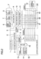
- the driving apparatus for a plasma display panel shown includes a scanning electrode driver 16, a write electrode driver 11 and a common electrode driver 12 for a main scanning electrode set 50, a write electrode set 51 and a common electrode set 52 of a plasma display panel PDP, respectively.
- the scanning electrode set 16 includes a pulse generator 13 for generating various pulse signals, a maintaining pulse generator 14 for generating a maintaining pulse signal, and a switching circuit 15 for selectively outputting one of an output pulse signal of the pulse generator 13 and the maintaining pulse signal from the maintaining pulse generator 14.
- the scanning electrode set 50 is driven by a maintaining voltage (Vs) power supply 2 and drives the scanning electrode set 50 in accordance with the pulse signal selected by the switching circuit 15. Meanwhile, the write electrode driver 11 is driven by a discharging voltage (Vd) power supply 5 and drives the write electrode set 51 in accordance with a normal signal (normal image signal) originated from a normal signal inputting section 6 and processed by a signal processing circuit 10.
- Vs maintaining voltage
- Vd discharging voltage
- confirmation of those cells which should emit light and those cells which should not emit light is automatically performed making use of discharge current and adjustment of a discharge maintaining voltage or a writing voltage is performed automatically.
- a driving apparatus for a plasma display panel wherein discharging gas is filled and enclosed between two glass plates and a plurality of scanning electrodes are provided in a horizontal direction while a plurality of write electrodes are provided in a vertical direction on inner faces of the glass plates and wherein a voltage is selectively applied between the electrodes to cause cells defined by the scanning electrodes and the write electrodes to discharge and emit light, comprising discharging situation detection means for detecting a variation of a state of each of the cells which has an influence on a display quality such as a temperature, an elapsed time or the like of the cell, and control means for calculating an optimum driving voltage for the scanning electrode or the write electrode of the cell in response to the discharging situation of the cell detected by the discharging situation detection means and causing the optimum driving voltage to be applied to the scanning electrode or the write electrode of the cell to cause the cell to discharge.
- discharging situation detection means for detecting a variation of a state of each of the cells which has an influence on a display quality such as
- the control means may calculate an optimum voltage necessary to drive the scanning electrode and apply the optimum voltage to the scanning electrode.
- the discharging situation detection means may include a current detection circuit for detecting current to flow to the scanning electrode and an integration circuit for integrating the detection current of the current detection circuit
- the control means may include a microcomputer which calculates the optimum voltage necessary to drive the scanning electrode from an output of the integration circuit and controls a voltage of a power supply for the scanning electrode.
- the control means may calculate an optimum voltage necessary to drive the write electrode and applies the optimum voltage to the write electrode.
- the discharging situation detection means may include a current detection circuit for detecting current to flow to the scanning electrode and an integration circuit for integrating the detection current of the current detection circuit
- the control means may include a signal switching circuit for first inputting an all-black signal and then inputting an all-white signal as a testing signal for detection of the discharging situation to a driver for the write electrode, and a microcomputer for calculating an optimum voltage necessary to drive the write electrode from an output of the integration circuit when the all-black signal is inputted and an output of the integration circuit when the all-white signal is inputted and controlling a voltage of a power supply for the write electrode to the optimum voltage.
- the plasma display panel driving apparatus exhibits various superior effects.
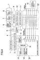
- the plasma display panel PDP in which the driving apparatus is incorporated includes a main scanning electrode set 50, a write electrode set 51 and a common electrode set 52 similar to those described hereinabove with reference to FIG. 5.
- the driving apparatus for the plasma display panel PDP includes a maintaining voltage (Vs) power supply 2, a scanning electrode driver 16 which in turn includes a pulse generator 13, a maintaining pulse generator 14 and a switching circuit 15, a write electrode driver 11, a common electrode driver 12, a discharging voltage (Vd) power supply 5, a normal signal inputting section 6, and a signal processing circuit 10, which are all similar to those of FIG. 5 described hereinabove.
- Vs maintaining voltage
- Vd discharging voltage
- the plasma display panel further includes a microcomputer 1, a current detection circuit 3, an integration circuit 4, a testing circuit T, and a switching circuit 9.
- a discharge maintaining voltage Vs of the maintaining voltage (Vs) power supply 2 is controlled.
- the current detection circuit 3 is additionally provided for a power supply to the scanning electrode driver 16 for the plasma display panel PDP. Further, since discharge current has a pulse waveform, the integration circuit 4 is additionally provided so that a discharging state can be detected. Furthermore, in order to provide a predetermined write signal to the write electrode driver 11, the switching circuit 9 for inputting an all-black signal 7 and an all-white signal 8 from the testing circuit T as a test signal for detection of a discharging situation to the signal processing circuit 10 is additionally provided in a stage preceding to the signal processing circuit 10.
- the microcomputer 1 is additionally provided to control the current detection circuit 3, integration circuit 4 and switching circuit 9 so that detection of discharge current by the current detection circuit 3, switching of an input signal to the signal processing circuit 10 among the all-white signal 8, the all-black signal 7 and a normal signal from the normal signal inputting section 6 by the switching circuit 9, controlling of the maintaining voltage, reading of the maintaining voltage (Vs), calculation of an optimum maintaining voltage, and variation of the maintaining voltage (VS) of the maintaining voltage (Vs) power supply 2 can be performed using a program installed in the microcomputer 1.
- a signal to be inputted to the signal processing circuit 10 is switched from the normal signal from the normal signal inputting section 6 to the all-black signal 7 from the testing circuit T by the switching circuit 9 under the control of the control microcomputer 1 (step S1), and then the maintaining voltage Vs is set to the lowest voltage thereof by the maintaining voltage (Vs) power supply 2 under the control of the microcomputer 1 (step S2).
- the screen of the plasma display panel PDP exhibits an all-black state wherein all of the cells do not emit light.
- the voltage applied to the cell is equal to a Vs + Vd set value, and current in the glow discharge region flows and the voltage can move to another point B illustrated in FIG. 1.
- step S3 while current detection is successively performed by the current detection circuit 3 (step S3), the maintaining voltage Vs is raised gradually (step S4) to detect the maintaining voltage Vs immediately before the cell begins to emit light (the voltage immediately before current detection is performed). Then, the detected voltage value M1 is stored into a memory in the microcomputer 1.
- step S6 the input signal to the signal processing circuit 10 is switched to the all-white signal 8 (step S6), and now, the maintaining voltage Vs is set to the highest value thereof (step S7). Then, while current detection is successively performed by the current detection circuit 3 (step S8), the maintaining voltage Vs is gradually lowered (step S9) to detect the maintaining voltage Vs immediately before the discharge current begins to decrease. Then, the detected voltage value M2 is stored into the memory of the microcomputer 1 (step S10).
- an optimum voltage value of the maintaining voltage Vs is calculated from the two voltage values M1 and M2 stored in the memory of the microcomputer 1 (step S11). Finally, the input signal to the signal processing circuit 10 is switched back to the normal signal from the normal signal inputting section 6.
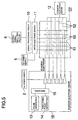
- FIG. 4 shows a modification to the driving apparatus for a plasma display panel described hereinabove with reference to FIG. 2.
- the write discharge maintaining voltage Vd for vertical lines by the discharging voltage (Vd) power supply 5 is varied under the control of the microcomputer 1 to detect a light emitting discharging situation. Then, the optimum write discharge voltage Vd necessary for driving is calculated and variable control of the write voltage Vd is performed in response to a result of the calculation. Also in this instance, similar effects to those described above can be obtained.
Landscapes
- Engineering & Computer Science (AREA)
- Physics & Mathematics (AREA)
- Computer Hardware Design (AREA)
- General Physics & Mathematics (AREA)
- Theoretical Computer Science (AREA)
- Control Of Indicators Other Than Cathode Ray Tubes (AREA)
- Transforming Electric Information Into Light Information (AREA)
- Devices For Indicating Variable Information By Combining Individual Elements (AREA)
- Control Of Gas Discharge Display Tubes (AREA)
Applications Claiming Priority (2)
| Application Number | Priority Date | Filing Date | Title |
|---|---|---|---|
| JP11088964A JP2000284743A (ja) | 1999-03-30 | 1999-03-30 | プラズマディスプレイパネル駆動装置 |
| JP8896499 | 1999-03-30 |
Publications (1)
| Publication Number | Publication Date |
|---|---|
| EP1047040A1 true EP1047040A1 (fr) | 2000-10-25 |
Family
ID=13957519
Family Applications (1)
| Application Number | Title | Priority Date | Filing Date |
|---|---|---|---|
| EP20000105667 Withdrawn EP1047040A1 (fr) | 1999-03-30 | 2000-03-17 | Appareil de commande pour un panneau d'affichage à plasma |
Country Status (3)
| Country | Link |
|---|---|
| US (1) | US6288495B1 (fr) |
| EP (1) | EP1047040A1 (fr) |
| JP (1) | JP2000284743A (fr) |
Cited By (6)
| Publication number | Priority date | Publication date | Assignee | Title |
|---|---|---|---|---|
| EP1278176A2 (fr) * | 2001-06-27 | 2003-01-22 | Fujitsu Hitachi Plasma Display Limited | Panneau d'affichage à plasma |
| WO2003107317A1 (fr) * | 2002-06-14 | 2003-12-24 | Thomson Licensing S.A. | Compensation de remanence pour panneaux d'affichage plasma |
| EP1394763A1 (fr) * | 2002-08-07 | 2004-03-03 | Conrac GmbH | Procédé et dispositif pour la compensation de la dégradation de la lumière de sortie d'un moniteur d'affichage |
| EP1271464A3 (fr) * | 2001-06-29 | 2004-10-20 | Pioneer Corporation | Dispositif d'affichage à plasma |
| US7102596B2 (en) | 2002-09-12 | 2006-09-05 | Lg Electronics Inc. | Method and apparatus for driving plasma display panel |
| US7538748B2 (en) | 2001-10-25 | 2009-05-26 | Lg Electronics Inc. | Apparatus and method for driving plasma display panel |
Families Citing this family (11)
| Publication number | Priority date | Publication date | Assignee | Title |
|---|---|---|---|---|
| JP3270435B2 (ja) | 1999-10-04 | 2002-04-02 | 松下電器産業株式会社 | 表示装置およびその輝度制御方法 |
| US6911783B2 (en) | 2000-10-25 | 2005-06-28 | Matsushita Electric Industrial Co., Ltd. | Drive method for plasma display panel and drive device for plasma display panel |
| EP1346339A2 (fr) * | 2000-12-20 | 2003-09-24 | Koninklijke Philips Electronics N.V. | Dispositif et procede d'affichage matriciel |
| JP4667619B2 (ja) * | 2001-02-27 | 2011-04-13 | パナソニック株式会社 | プラズマ表示装置及びその駆動方法 |
| JP4843156B2 (ja) * | 2001-06-13 | 2011-12-21 | 株式会社日立国際電気 | 表示装置 |
| KR100462600B1 (ko) * | 2002-04-02 | 2004-12-20 | 삼성전자주식회사 | 디스플레이 패널 구동 시스템의 전원 자동 조정 제어 장치및 방법 |
| JP2005308917A (ja) * | 2004-04-20 | 2005-11-04 | Hitachi Ltd | プラズマディスプレイ装置 |
| JPWO2007015309A1 (ja) * | 2005-08-04 | 2009-02-19 | 日立プラズマディスプレイ株式会社 | プラズマディスプレイ装置 |
| US20090079722A1 (en) * | 2005-08-04 | 2009-03-26 | Makoto Onozawa | Plasma display device |
| KR100671208B1 (ko) * | 2005-08-19 | 2007-01-19 | 삼성전자주식회사 | 전자장치 및 그 제어방법 |
| KR100680224B1 (ko) * | 2005-09-22 | 2007-02-08 | 엘지전자 주식회사 | 플라즈마 디스플레이 장치 및 그 구동방법 |
Citations (2)
| Publication number | Priority date | Publication date | Assignee | Title |
|---|---|---|---|---|
| US4017762A (en) * | 1974-12-04 | 1977-04-12 | Ibm Corporation | Voltage controlled sustain frequency in a gas display panel |
| US4079290A (en) * | 1976-05-27 | 1978-03-14 | International Business Machines Corporation | Gas panel voltage regulator |
Family Cites Families (8)
| Publication number | Priority date | Publication date | Assignee | Title |
|---|---|---|---|---|
| US5233272A (en) * | 1991-08-30 | 1993-08-03 | Samsung Electron Devices, Co., Ltd. | DC plasma display panel and driving method thereof |
| JP2853537B2 (ja) * | 1993-11-26 | 1999-02-03 | 富士通株式会社 | 平面表示装置 |
| US5956014A (en) * | 1994-10-19 | 1999-09-21 | Fujitsu Limited | Brightness control and power control of display device |
| US5638085A (en) * | 1995-01-13 | 1997-06-10 | Micron Display Technology, Inc. | Timing control for a matrixed scanned array |
| EP0755043B1 (fr) * | 1995-07-21 | 2009-09-02 | Canon Kabushiki Kaisha | Circuit de commande d'échelle des gris avec compensation de la luminance |
| US6100859A (en) * | 1995-09-01 | 2000-08-08 | Fujitsu Limited | Panel display adjusting number of sustaining discharge pulses according to the quantity of display data |
| JP3408684B2 (ja) * | 1995-12-25 | 2003-05-19 | 富士通株式会社 | プラズマディスプレイパネルの駆動方法及びプラズマディスプレイ装置 |
| JP3348610B2 (ja) * | 1996-11-12 | 2002-11-20 | 富士通株式会社 | プラズマディスプレイパネルの駆動方法及び装置 |
-
1999
- 1999-03-30 JP JP11088964A patent/JP2000284743A/ja active Pending
-
2000
- 2000-03-17 US US09/528,440 patent/US6288495B1/en not_active Expired - Fee Related
- 2000-03-17 EP EP20000105667 patent/EP1047040A1/fr not_active Withdrawn
Patent Citations (2)
| Publication number | Priority date | Publication date | Assignee | Title |
|---|---|---|---|---|
| US4017762A (en) * | 1974-12-04 | 1977-04-12 | Ibm Corporation | Voltage controlled sustain frequency in a gas display panel |
| US4079290A (en) * | 1976-05-27 | 1978-03-14 | International Business Machines Corporation | Gas panel voltage regulator |
Cited By (13)
| Publication number | Priority date | Publication date | Assignee | Title |
|---|---|---|---|---|
| EP1278176A3 (fr) * | 2001-06-27 | 2004-11-10 | Fujitsu Hitachi Plasma Display Limited | Panneau d'affichage à plasma |
| CN100367331C (zh) * | 2001-06-27 | 2008-02-06 | 富士通日立等离子显示器股份有限公司 | 等离子体显示装置 |
| EP1278176A2 (fr) * | 2001-06-27 | 2003-01-22 | Fujitsu Hitachi Plasma Display Limited | Panneau d'affichage à plasma |
| US6954186B2 (en) | 2001-06-29 | 2005-10-11 | Pioneer Corporation | Plasma display panel unit |
| EP1271464A3 (fr) * | 2001-06-29 | 2004-10-20 | Pioneer Corporation | Dispositif d'affichage à plasma |
| US7538748B2 (en) | 2001-10-25 | 2009-05-26 | Lg Electronics Inc. | Apparatus and method for driving plasma display panel |
| US8471784B2 (en) | 2001-10-25 | 2013-06-25 | Lg Electronics Inc. | Apparatus and method for driving plasma display panel |
| EP1376520A1 (fr) * | 2002-06-14 | 2004-01-02 | Deutsche Thomson Brandt | Compensation pour la rémanence d'image sur un panneau d'affichage à plasma |
| WO2003107317A1 (fr) * | 2002-06-14 | 2003-12-24 | Thomson Licensing S.A. | Compensation de remanence pour panneaux d'affichage plasma |
| EP1394763A1 (fr) * | 2002-08-07 | 2004-03-03 | Conrac GmbH | Procédé et dispositif pour la compensation de la dégradation de la lumière de sortie d'un moniteur d'affichage |
| US7102596B2 (en) | 2002-09-12 | 2006-09-05 | Lg Electronics Inc. | Method and apparatus for driving plasma display panel |
| EP1398756A3 (fr) * | 2002-09-12 | 2007-12-26 | Lg Electronics Inc. | Procédé et dispositif de commande d'un panneau d'affichage à plasma |
| US7348938B2 (en) | 2002-09-12 | 2008-03-25 | Lg Electronics Inc. | Method and apparatus for driving plasma display panel |
Also Published As
| Publication number | Publication date |
|---|---|
| US6288495B1 (en) | 2001-09-11 |
| JP2000284743A (ja) | 2000-10-13 |
Similar Documents
| Publication | Publication Date | Title |
|---|---|---|
| US6288495B1 (en) | Driving apparatus for plasma display panel | |
| JP3672697B2 (ja) | プラズマディスプレイ装置 | |
| US6278436B1 (en) | Brightness controlling apparatus | |
| KR100389643B1 (ko) | 표시장치와 그 표시제어기 및 그 표시장치의 제어방법 | |
| KR100439062B1 (ko) | 표시 유니트의 소비 전력 제어방법과 장치, 그 장치를 포함하는 표시 시스템, 및 그 방법을 실현하는 프로그램을 저장한 기억 매체 | |
| US7133008B2 (en) | Drive method and drive apparatus for a display panel | |
| US6650307B1 (en) | Method of driving display panel and panel display apparatus | |
| EP1124217A2 (fr) | Méthode et dispositif de commande de puissance pour un panneau d'affichage à plasma | |
| JP4010510B2 (ja) | プラズマ表示パネルのアドレスデータ自動電力制御方法,その装置,及びその装置を有するプラズマ表示パネル | |
| KR100279044B1 (ko) | Pdp의유지펄스제어장치 | |
| US20060077131A1 (en) | Driving apparatus for display panel and control method of the driving apparatus | |
| JPH09138668A (ja) | 表示装置 | |
| KR100432668B1 (ko) | 플라즈마 표시 패널의 구동 전력을 제어하는 방법과 장치,그 장치를 포함하는 플라즈마 표시 패널 장치 | |
| JP2001075529A (ja) | 表示装置およびその輝度制御方法 | |
| KR20090016579A (ko) | 플라즈마 디스플레이 장치 및 플라즈마 디스플레이 패널의 구동 방법 | |
| EP1494200A2 (fr) | Dispositif d'affichage | |
| KR20000000730A (ko) | 플라즈마 디스플레이 패널의 구동장치 | |
| US7528806B2 (en) | Plasma display panel and method for driving the same | |
| KR100570599B1 (ko) | 플라즈마 표시 패널의 소비 전력을 제어하는 방법과 장치,그 장치를 포함하는 플라즈마 표시 패널 장치 | |
| KR100491836B1 (ko) | 플라즈마 디스플레이 패널의 평균화상레벨 제어방법 및 장치 | |
| KR100437334B1 (ko) | 플라즈마 표시 패널의 구동 전력 제어 방법과 장치, 그장치를 갖는 플라즈마 표시 패널 장치 | |
| KR100486504B1 (ko) | 디스플레이 소자 구동 장치 | |
| US20060170618A1 (en) | Driving method and driving circuit of plasma display panel | |
| KR100480165B1 (ko) | 다이나믹 레인지 확대방법을 이용한 플라즈마 디스플레이패널의 구동장치 및 방법 | |
| KR100280887B1 (ko) | 플라즈마디스플레이패널의구동장치 |
Legal Events
| Date | Code | Title | Description |
|---|---|---|---|
| PUAI | Public reference made under article 153(3) epc to a published international application that has entered the european phase |
Free format text: ORIGINAL CODE: 0009012 |
|
| AK | Designated contracting states |
Kind code of ref document: A1 Designated state(s): DE FR |
|
| AX | Request for extension of the european patent |
Free format text: AL;LT;LV;MK;RO;SI |
|
| 17P | Request for examination filed |
Effective date: 20010122 |
|
| AKX | Designation fees paid |
Free format text: DE FR |
|
| RAP1 | Party data changed (applicant data changed or rights of an application transferred) |
Owner name: NEC PLASMA DISPLAY CORPORATION |
|
| RAP1 | Party data changed (applicant data changed or rights of an application transferred) |
Owner name: PIONEER PLASMA DISPLAY CORPORATION |
|
| RAP1 | Party data changed (applicant data changed or rights of an application transferred) |
Owner name: PIONEER CORPORATION |
|
| 17Q | First examination report despatched |
Effective date: 20071122 |
|
| STAA | Information on the status of an ep patent application or granted ep patent |
Free format text: STATUS: THE APPLICATION IS DEEMED TO BE WITHDRAWN |
|
| 18D | Application deemed to be withdrawn |
Effective date: 20080403 |