EP1045519A2 - Predriver circuit for controlling a power drive circuit - Google Patents
Predriver circuit for controlling a power drive circuit Download PDFInfo
- Publication number
- EP1045519A2 EP1045519A2 EP00200947A EP00200947A EP1045519A2 EP 1045519 A2 EP1045519 A2 EP 1045519A2 EP 00200947 A EP00200947 A EP 00200947A EP 00200947 A EP00200947 A EP 00200947A EP 1045519 A2 EP1045519 A2 EP 1045519A2
- Authority
- EP
- European Patent Office
- Prior art keywords
- circuit
- analog
- analog signal
- output
- signal
- Prior art date
- Legal status (The legal status is an assumption and is not a legal conclusion. Google has not performed a legal analysis and makes no representation as to the accuracy of the status listed.)
- Withdrawn
Links
Images


Classifications
-
- H—ELECTRICITY
- H03—ELECTRONIC CIRCUITRY
- H03K—PULSE TECHNIQUE
- H03K17/00—Electronic switching or gating, i.e. not by contact-making and –breaking
- H03K17/06—Modifications for ensuring a fully conducting state
- H03K17/063—Modifications for ensuring a fully conducting state in field-effect transistor switches
-
- H—ELECTRICITY
- H03—ELECTRONIC CIRCUITRY
- H03K—PULSE TECHNIQUE
- H03K17/00—Electronic switching or gating, i.e. not by contact-making and –breaking
- H03K17/16—Modifications for eliminating interference voltages or currents
- H03K17/161—Modifications for eliminating interference voltages or currents in field-effect transistor switches
- H03K17/165—Modifications for eliminating interference voltages or currents in field-effect transistor switches by feedback from the output circuit to the control circuit
- H03K17/166—Soft switching
-
- H—ELECTRICITY
- H03—ELECTRONIC CIRCUITRY
- H03K—PULSE TECHNIQUE
- H03K2217/00—Indexing scheme related to electronic switching or gating, i.e. not by contact-making or -breaking covered by H03K17/00
- H03K2217/0036—Means reducing energy consumption
-
- H—ELECTRICITY
- H03—ELECTRONIC CIRCUITRY
- H03K—PULSE TECHNIQUE
- H03K2217/00—Indexing scheme related to electronic switching or gating, i.e. not by contact-making or -breaking covered by H03K17/00
- H03K2217/0063—High side switches, i.e. the higher potential [DC] or life wire [AC] being directly connected to the switch and not via the load
-
- H—ELECTRICITY
- H03—ELECTRONIC CIRCUITRY
- H03K—PULSE TECHNIQUE
- H03K2217/00—Indexing scheme related to electronic switching or gating, i.e. not by contact-making or -breaking covered by H03K17/00
- H03K2217/0081—Power supply means, e.g. to the switch driver
Definitions
- the present invention relates generally to predriver circuits operable to control the operation of power drive circuits, and more specifically to such predriver circuits used in high voltage applications such as, for example, in controlling the operation of DC motors.
- a motor control circuit is typically operable to detect motor shaft position as well as motor drive current, and a motor drive circuit is, in turn, responsive to motor control signals supplied by the motor control circuitry to drive the DC motor in a desired manner.
- the motor driving function is often partitioned into a two-stage drive operation; namely a pre-driver circuit and a power drive circuit.
- the pre-driver circuit typically serves as an interface between a motor control logic circuit and a power drive device such as a discrete power transistor, wherein the pre-driver circuit is operable to convert the logic level motor control signals to one or more signals suitable for driving the power drive device.
- a predriver circuit for controlling a power drive circuit comprises a turn on drive circuit having a first analog input adapted to receive a first analog signal and an analog output adapted for connection to an input of a power drive circuit, wherein the turn on drive circuit is responsive to one of an active and an inactive state of a first digital signal to supply an amplified representation of the first analog signal to the analog output.
- the turn on drive circuit is further responsive to the other of an active and an inactive state of the first digital control signal to disable supply of the amplified representation of the first analog signal to the analog output.
- a turn off drive circuit having a second analog input adapted to receive a second analog signal and an analog output defined by the analog output of the turn on drive circuit, wherein the turn off drive circuit is responsive to the other of an active and inactive state of the first digital control signal to draw an amplified representation of the second analog signal from the analog output.
- the turn off drive circuit is further responsive to the one of an active and an inactive state of the first digital control signal to disable draw of the amplified representation of the second analog signal from the analog output.
- a predriver circuit for controlling a power drive circuit comprises a first analog signal amplifier defining an input adapted to receive a first analog signal and a second analog signal amplifier coupled to the first analog signal amplifier and defining an output adapted for connection to an input of a power drive circuit, wherein the first and second analog amplifiers are responsive to a first state of a predriver control signal to supply an amplified representation of the first analog signal to the output.
- a sense circuit is included and is responsive to detection of the amplified representation of the first analog signal to disable operation of the first analog signal amplifier and a first portion of the second analog amplifier to thereby reduce electrical power consumed thereby.
- control circuit responsive to disablement of the first analog signal amplifier to maintain a second portion of the second analog amplifier operable to thereby maintain the output near a predefined signal level for a duration of the first state of the predriver control signal.
- a turn off drive circuit is further included and is responsive to a second state of the predriver control signal to draw a second analog signal from the output.
- a predriver circuit for controlling a power drive circuit comprises a turn on drive circuit responsive to a first state of a predriver control signal to supply a first analog signal to a predriver circuit output thereof, wherein the predriver circuit output is adapted for connection to an input of a power drive circuit, a first analog signal amplifier defining an input adapted to receive a second analog signal, a second analog signal amplifier having an input coupled to the first analog signal amplifier and defining a second amplifier output, a third analog signal amplifier coupled to the second amplifier output and defining an output connected to the predriver circuit output, wherein the first, second and third amplifiers are responsive to a second opposite state of the predriver control signal to draw an amplified representation of the second analog signal from the predriver circuit output, a sense circuit responsive to detection of the amplified representation of the second analog signal drawn from the predriver circuit output to disable operation of the first and second analog signal amplifiers and a first portion of the third analog signal amplifier to thereby
- a predriver circuit for controlling a power drive circuit comprises a turn on drive circuit having a first analog input adapted to receive a first analog signal and an analog output adapted for connection to an input of a power drive circuit, wherein the turn on drive circuit is responsive to one of an active and an inactive state of a first digital signal to supply an amplified representation of the first analog signal to the analog output and to produce a digital turn off circuit disable signal.
- a turn off drive circuit having a second analog input adapted to receive a second analog signal and an analog output defined by the analog output of the turn on drive circuit, wherein the turn off drive circuit is responsive to the other of an active and inactive state of the first digital control signal to draw an amplified representation of the second analog signal from the analog output and to produce a digital turn on circuit disable signal.
- the turn on circuit is further responsive to the digital turn on circuit disable signal to disable operation thereof by disabling supply of the amplified representation of the first analog signal to the analog output
- the turn off circuit is further responsive to the digital turn off circuit disable signal to disable operation thereof by disabling draw of the amplified representation of the second analog signal from the analog output.
- One object of the present invention is to provide an improved predriver circuit for controlling operation of a motor drive circuit.
- Another object of the present invention is to provide such an improved predriver circuit capable of high speed operation in a high voltage environment while also minimizing power dissipation.
- Yet another object of the present invention is to provide an improved predriver circuit that operates in a high voltage environment while also satisfying imposed EMI requirements.
- System 10 includes a DC motor 22, which is preferably a known brushless DC motor, operable to drive a rotor or output shaft 26 thereof as is known in the art.
- Motor 22 is electrically connected to a power driver circuit 18 via a number, K, of signal paths 24, wherein K may be any integer.
- Power driver circuit 18 is, in turn, electrically connected to a motor driver control circuit 14 via a corresponding number, K, of signal paths 20.
- Motor driver control circuit 14 is, in turn, electrically connected to a motor control circuit 12 via a number, N, of signal paths 16, wherein N may be any integer.
- a motor position sense circuit 21 is associated with motor 22 and is electrically connected to motor control circuit 12 via a number, J, of signal paths 27, wherein J may be any integer.
- Motor position sense circuit 21 is operable to sense a position of rotor 26 relative to a motor armature (not shown) in a known manner, and in one preferred embodiment motor position sense circuit 21 includes a number of Hall effect sensors operable to sense rotor position and provide a corresponding number of rotor position signals on signal path 27 as is known in the art.
- sense circuit 21 may include a number of other known sensors or sensing circuits operable to sense rotor position and produce a corresponding number of rotor position signals, an example of which includes, but is not limited to, a variable reluctance sensor. In either case, motor position sense circuit 21 is operable to provide a number, J, of motor position signals to motor control circuit 12 via a corresponding number, J, of signal paths 27.
- a motor current detection circuit 23 is electrically connected to the power driver circuit 18 via a number, L, of signal paths 19, wherein L may be any integer, and is also connected to motor control circuit 12 via a corresponding number, L, of signal paths 29.
- motor winding current I M is directed through one or more sense resistors R SENSE , wherein a corresponding sense voltage developed thereacross is provided to motor current detection circuit 23, although the present invention contemplates that the motor winding current I M may be alternatively sensed by other known techniques wherein one or more signals corresponding to motor winding current are provided to motor current detection circuit 23.
- Motor current detection circuit 23 preferably includes a sense amplifier circuit of the type described in co-pending U.S. Patent Application Ser. No.
- motor control circuit 12 is a microprocessor or microprocessor-based control circuit operable to control motor driver control circuit 14 based, at least in part, on the one or more motor current signals provided thereto by motor current detection circuit 23 and on the one or more motor position signals provided thereto by motor position sense circuit 21. In any case, motor control circuit 12 is operable to control the operation of motor 22 via appropriate control signals provided to motor driver control circuit 14 via signal paths 16.
- motor driver control circuit 14 is operable to provide appropriate pre-drive signals on signal paths 20, whereby the power driver circuit 18 is responsive to such signals to drive motor 22 to thereby actuate rotor 26 in a desired manner as is known in the art.
- the motor driver control circuit 14 includes a pre-driver circuit 25 that is electrically connected to power driver circuit 18 via the number, K, of signal paths 20, and is electrically connected to motor control circuit 12 of known construction via the number, N, of signal paths 16.
- a voltage supply (not shown) is operable to supply an electrical power signal VIGN (e.g., vehicle battery voltage or other desired voltage), wherein VIGN is connected to power driver circuit 18 and to a charge pump circuit 30 of known construction, and wherein charge pump circuit 30 forms part of motor driver control circuit 14.
- the charge pump circuit 30 is electrically connected to predriver circuit 25 via a number, M, of signal paths 32, whereby charge pump circuit 30 is operable to supply predriver circuit 25 with one or more DC supply voltages as is known in the art.
- Both the charge pump circuit 80 and the predriver circuit 25 are referenced to ground potential via signal path 34.
- FIG. 2 a simplified diagram of one preferred embodiment of the motor driver control circuit 14 and power driver circuit 18, in accordance with the present invention, are shown.
- the predriver circuit 25 is partitioned into a turn-on drive circuit 25 1 and a turn-off drive circuit 25 2 , wherein the two subcircuits 25 1 and 25 2 are in electrical communication with each other via a number, J, of signal paths 36 1 , 36 2 ,..., 36 J as will be described more fully hereinafter.
- Turn-on drive circuit 25 1 defines a first input IN 1 adapted to receive a first input signal from motor control circuit 12 via signal path 16 1 and a second input VCLK adapted to receive a second input signal from motor control circuit 12 via signal path 16 2 .
- the first input signal received by turn-on drive circuit 25 1 at input IN 1 is a substantially constant-valued analog current signal I1, although the present invention contemplates that the first input signal may alternatively be a current signal that is varying or variable in accordance with a desired variation criteria.
- the second input signal received by turn-on drive circuit 25 1 at input VCLK is preferably a digital control signal operable to control turn-on and turn-off operation of both circuits 25 1 and 25 2 as will be described in greater detail hereinafter.
- the VCLK signal is accordingly provided to the turn-off drive circuit 25 2 via one of the signal paths 36 J as will be subsequently described.
- Turn-off drive circuit 25 2 defines a first input IN2 adapted to receive a third input signal from motor control circuit 12 via signal path 16 3 and a second input PWMBF adapted to receive a fourth input signal from motor control circuit 12 via signal path 16 4 .
- the third input signal received by turn-off drive circuit 25 2 at input IN2 is a substantially constant-valued analog current signal I2, although the present invention contemplates that the third input signal may alternatively be a current signal that is varying or variable in accordance with a desired variation criteria.
- the fourth input signal received by turn-off drive circuit 25 2 at input PWMBF is preferably a digital control signal that is asserted whenever motor 22 is active; i.e., whenever motor position determination circuit 12 is operable to command operation of motor 22.
- the PWMBF signal is provided to turn-on drive circuit 25 1 for control thereof via one of the signal paths 36 J as will be subsequently described.
- the charge pump circuit 30 is responsive to the VIGN supply signal to produce a first high voltage level HV1 on signal path 32 1 and a second high voltage level HV2 on signal path 32 2 .
- VIGN is nominally 12.0 volts (although VIGN may be any desired voltage)
- charge pump circuit 30 is operable to produce a HV1 voltage of approximately 30 volts and a HV2 voltage of approximately 15 volts, although the present invention contemplates other values of HV1 and HV2.
- boost voltages HV1 and HV2 are supplied by remote voltage sources (not shown) so that charge pump circuit 30 may be omitted from motor driver control circuit 14.
- turn-on drive circuit 25 1 and turn-off drive circuit 25 2 define a common output that produces an output signal VOUT suitable for controlling/driving a load such as the power driver circuit 18.
- the power driver circuit 18, in the embodiment illustrated in FIG. 2, includes at least one power transistor such as a power metal oxide semiconductor field effect transistor (power MOSFET) suitable for driving motor 22 from VIGN supply. It is to be understood, however, that the power driver circuit 18 may alternatively or additionally include one or more power bipolar junction transistors (power BJT), insulated gate bipolar transistors (IGBT) or other known transistor variations, as well as one or more relays and/or other suitable switching devices, although power driver circuit 18 will be described hereinafter for the purpose of brevity as including only a single power MOSFET 40.
- the output of motor driver control circuit 14 is electrically connected to the gate 38 of MOSFET 40 via signal path 20 1 , and the drain 42 of MOSFET 40 is connected to the VIGN supply.
- the source 44 of MOSFET 40 is electrically connected to motor 22 via signal path 24, and to a phase input PH of turn-off drive circuit 25 2 via signal path 20 2 .
- the turn-on drive circuit 25 1 is responsive to a first state of the digital VCLK signal to amplify the input current I1 received at input IN1 and supply ⁇ *I1 source current to VOUT (and accordingly to the gate 38 of MOSFET 40), wherein ⁇ is the gain of turn-on drive circuit 25 1 , while the turn-off drive circuit 25 2 is responsive to the first state of the digital VCLK signal to disable operation thereof.
- the turn-off drive circuit 25 2 is responsive to a second opposite state of the digital VCLK signal to amplify the input current I2 received at input IN2 and draw a current ⁇ *I2 from VOUT (and accordingly from the gate 38 of MOSFET 40), wherein ⁇ is the gain of turn-off drive circuit 25 2 , while the turn-on drive circuit 25 1 is responsive to the second opposite state of the digital VCLK signal to disable operation thereof.
- the predriver circuit 25 is thus preferably partitioned into two subcircuits; namely a turn-on drive circuit 25 1 and turn-off drive circuit 25 2 , whereby the turn-on circuit 25 1 is operable to turn on MOSFET 40 and the turn-off drive circuit 25 2 is operable to turn off MOSFET 40.
- Both subcircuits 25 1 and 25 2 are preferably configured for digital control and communication therebetween and also with the motor position determination circuit 16 so that the partitioned high voltage switching operation of MOSFET 40 may be carried out at high speed.
- the turn-on drive circuit 25 1 and turn-off drive circuit 25 2 are preferably configured to control MOSFET 40 as just described while minimizing the amount of electrical power drawn from supply HV1 by each subcircuit 25 1 and 25 2 .
- input currents I1 and I2 received at inputs IN1 and IN2 respectively are preferably constant-valued (DC) currents.
- the respective magnitudes of I1 and I2 determine, at least in part, both the rise and fall times (slew rate) of the output signal VOUT provided on signal path 20 1 as well as the electromagnetic interference (EMI) generated by motor driver control circuit 14.
- slew rate the rise and fall times
- EMI electromagnetic interference
- lower I1 and I2 values correspond to lower generated EMI values, but also to slower slew rates.
- higher I1 and I2 values correspond to faster slew rates, but also to higher generated EMI values.
- the current values I1 and I2 are chosen to optimize a trade-off between slew rate and EMI requirements, and those skilled in the art will recognize that the I1 and I2 values chosen will typically be dictated by slew rate and EMI requirements of the particular application of motor driver control circuit 14.
- Input In1 (signal path 16 1 ) is connected to a gate and drain of a n-MOS transistor M42 and to the source of a p-MOS transistor M41.
- the gate of M41 is connected to the output of a NAND gate N1, to a first input of another NAND gate N5 and to the gate of a n-MOS transistor M40.
- the drain of M40 is connected to the drain of M41 and to the gate of a n-MOS transistor M39, and the sources of M39, M40 and M42 are connected to ground potential.
- the drain of M30 is connected to the source of a DMOS transistor DM1 having a gate connected to high voltage HV2 of charge pump circuit 30 via signal path 32 2 and also to signal path 36 1 leading to turn-off drive circuit 25 2 .
- a first input of N1 is connected to turn-off drive circuit 25 2 via signal path 36 2 and a second input of N1 is connected to a first input of a NAND gate N3, to a first input of another NAND gate N4, to a first input of yet another NAND gate N6, to a second input of N5, to input VCLK 16 2 and to turn-off drive circuit 25 2 via signal path 36 3 .
- a third input of N1 is connected to the output of N3 and to a first input of a NAND gate N2.
- the output of N2 is connected to a second input of N3, and a second input of N2 is connected to the output of N4.
- a second input of N4 is connected to an output of an inverter I4 having an input connected to an output of another inverter I3.
- a fourth input of N1 is connected to a third input of N5, to a second input of N6 and to turn-off drive circuit 25 2 via signal path 36 4 .
- the output of N5 is connected to the input of an inverter I1 having an output connected to the gate of a DMOS transistor DM3 and the output of N6 is connected to the gate of another DMOS transistor DM2.
- the source of DM2 is connected to one end of a resistor R5 having an opposite end connected to ground potential.
- the drain of DM2 is connected to the gate and drain of a p-MOS transistor M31, to the gate of another p-MOS transistor M32 and to the gate of yet another p-MOS transistor M29.
- the sources of M29, M31 and M32 are connected to high voltage HV1 provided by charge pump circuit 30 via signal path 32 1 .
- the drain of DM1 is connected to the drain of a n-MOS transistor M33, to the collector and base of a PNP transistor Q1, to the collector and base of another PNP transistor Q2 and to one end of a resistor R11.
- the emitter of Q2 is connected to the gate of M33 and to the drain of M32, and the source of M33 is connected to HV1 via signal path 32 1 .
- the emitter of Q1 is connected to the drain of M29, to one end of a resistor R9, to one end of a resistor R10, to the gate of a p-MOS transistor M30 and to the gate of a p-MOS transistor M1.
- R9 is connected to the anode of a diode D1 having a cathode connected to the anode of another diode D2 having a cathode connected to the cathode of still another diode D3.
- the cathode of D3 is connected to the source of M1 and to HV1 via signal path 32 1 .
- the opposite end of R10 is connected to the drain of DM3 and the source of DM3 is connected to ground potential.
- the source of M30 is connected to one end of a resistor R14 having an opposite end connected to HV1 via signal path 32 1 .
- the drain of M30 is connected to one end of a resistor R6 and to the gate, to the drain of a n-MOS transistor M37 and to the input of an inverter gate I2 having an output connected to turn-off drive circuit 25 2 via signal path 36 5 .
- the opposite end of R6 and the source of M37 are connected to ground potential.
- the drain of M1 defines the output VOUT of pre-driver circuit 25 (signal path 20 1 ) and is connected to one end of a resistor R8.
- the opposite end of R8 is connected to the emitter of a PNP transistor Q4 having a base and collector connected to the source of a p-MOS transistor M34 and to the anode of a diode D4.
- the cathode of D4 is connected to the emitter of a NPN transistor Q3 having a base and collector connected to the opposite end of R11.
- the drain of M34 is connected to one end of a resistor R13, to the gate and drain of a transistor M36 and to the input of I3.
- the opposite end of R13 and the source of M36 are connected to ground potential.
- Transistors M39 and M42 define a first amplifier stage that may be activated and deactivated via control of M40.
- Transistors M33 and M1 define a second amplifier stage wherein the differential pair M33 and M1 are decoupled from each other via Q1 and Q2.
- the overall gain ⁇ of turn-on drive circuit 25 1 is defined by the physical size/area ratio of any of the devices M42, M39, M33 and M1.
- R8, Q4, M34, R13, M36, D4, Q3 and R11 define a sense circuit operable to sense the voltage level of VOUT and provide a digital signal corresponding thereto.
- M30, R14, R6, M37 and I2 define a control circuit operable to monitor the gate drive of M1 and provide a digital signal corresponding thereto.
- Input IN2 (signal path 16 3 ) is connected to the gate and drain of a n-MOS transistor M26 and to the source of a p-MOS transistor M44.
- the gate of M44 is connected to the gate of a n-MOS transistor M43, to the output of a NAND gate N13 and to a first input of another NAND gate N8.
- the drain of M43 is connected to the drain of M44 and to the gate of a n-MOS transistor M27.
- the sources of M26, M27 and M43 are connected to ground potential.
- the drain of M27 is connected to the source of a DMOS transistor DM3 having a gate connected to the high voltage line HV2 of turn-on drive circuit 25 1 via signal path 36 2 .
- the drain of DM3 is connected to the gate and drain of a p-MOS transistor M25 and to the gate of another p-MOS transistor M24.
- the sources of M24 and M25 are connected to the high voltage line HV1 of turn-on drive circuit 25 1 via signal path 36 6 .
- a first input of N13 is connected to a first input of a NAND gate N7, to a first input of another NAND gate N9, to input PWMBF (signal line 16 4 ) and to turn-on drive circuit 25 1 via signal path 36 4 .
- a second input of N13 is connected to turn-on drive circuit 25 1 via signal path 36 5 , and a third input of N13 is connected to the output of an inverter I7, a first input of another NAND gate N10 and to a first input of yet another NAND gate N12.
- a fourth input of N13 is connected to the output of N12 and to a first input of another NAND gate N11.
- the output of N11 is connected to a second input of N12 and a second input of N11 is connected to the output of N10.
- a second input of N10 is connected to the output of an inverter I5 having and input connected to the output of another inverter I6.
- the input of I6 is connected to the drain of a p-MOS transistor M23 and to the gate and drain of a n-MOS transistor M16 and to one end of a resistor R1.
- the opposite end of R1 and the source of M16 are connected to ground potential, and the source of M23 is connected to HV1 via signal path 36 6 .
- the input of I7 is connected to a second input of N7 and to turn-on drive circuit 25 1 via signal path 36 3 .
- the output of N7 is connected to a second input of N8 and to the gate of a DMOS transistor DM6 having a source connected to ground potential and a drain connected to one end of a resistor R3.
- the opposite end of R3 is connected to HV1 via signal path 36 6 .
- the output of N8 is connected to a second input of N9, wherein the output of N9 is connected to the gate of a DMOS transistor DM4 having a source coupled to ground potential through a resistor R4.
- the drain of DM4 is connected to the gate and drain of a p-MOS transistor M22 and to the gate of another p-MOS transistor M19.
- the drain of M24 is connected to the drain of a n-MOS transistor M14, to the base and collector of a NPN transistor D7, to the base and collector of another NPN transistor D8 and to the anode of a diode D5.
- the emitter of D7 is connected to the gate and drain of a transistor M10, to the gate of another n-MOS transistor M11, to the gate of M14, to the gate of another n-MOS transistor M8, to the gate of yet another n-MOS transistor M9, to the gate of a still another transistor M13 and to the drain of a further n-MOS transistor M12.
- the drain of M13 is connected to the source of M14 and the drain of M11 is connected to the source of M10, and the drain of M9 is connected to the source of M8.
- the sources of M9, M11, M12 and M13 are connected to phase input PH (signal path 20 2 ).
- the drain of M8 is connected to the gate and drain of a p-MOS transistor M20 and to the gate of another p-MOS transistor M21.
- the sources of M20 and M21 are connected to HV1 via signal path 36 6 .
- the drain of M21 is connected to the input of an inverter I8 having an output connected to the turn-on drive circuit 25 1 via signal path 36 1 .
- the emitter of D8 is connected to the drain of M19, to one end of a resistor R7, to the gate of a n-MOS transistor M2, to the gate of another n-MOS transistor M3, and to the drain of yet another n-MOS transistor M4.
- the drain of M3 is connected to the source of M2 and the drain of a n-MOS transistor M5 is connected to the source of M4.
- the gates of M4 and M5 are connected to the gate and drain of a n-MOS transistor M6 and to the gate of M12.
- the source of M6 is connected to the gate and drain of a n-MOS transistor M7 and the sources of M3, M5 and M7 are connected to phase input PH.
- the drain of M2 is connected to one end of a resistor R12 to turn-on drive circuit 25 1 via signal path 20 1 .
- the drain of M2 of turn-off drive circuit 25 2 and the drain of M1 of turn-on drive circuit 25 1 define the output VOUT of pre-driver circuit 25.
- the opposite end of R12 is connected to the source of a DMOS transistor DM5 having a drain connected to the gate and drain of a p-MOS transistor M18 and to the gate of M23.
- the source of M18 is connected to HV1 via signal path 36 6
- the gate of DM5 is connected to the cathode of D5 and to the emitter of a NPN transistor D6.
- the base and collector of D6 are connected to the opposite end of R7.
- Transistors M26 and M27 define a first amplifier stage of turn-off drive circuit 25 2 that may be activated and deactivated via control of M43.
- Transistors M25 and M24 define a second amplifier stage, and transistors M13/M14 and M2/M3 define a third amplifier stage, wherein the differential pairs M13/M14 and M2/M3 are decoupled from each other via D7 and D8.
- the overall gain ⁇ of turn-off circuit 25 2 is defined by the physical size/area ratio of any of the devices M24-M27, M13/M14 and M2/M3.
- R12, DM5, M18, M23, M16 and R1 define a sense circuit operable to sense the voltage level of VOUT and provide a digital signal corresponding thereto.
- M8-M11 and M20-21 define a control circuit operable to monitor the gate drive of M2/M3 and provide a digital signal corresponding thereto.
- pre-driver circuit 25 i.e., whether to drive VOUT high or low, is determined by the state of the VCLK signal, and the PWMBF signal is asserted whenever the motor 22 is active.
- PWMBF When VCLK transitions from a low to a high state and PWMBF is in an active (e.g., high) state, the gate of M40 is commanded low and the first amplifier stage of turn-on drive circuit 25 1 comprising M42 and M39 is activated.
- the gates of DM2 and DM3 are commanded low so that the devices M29, M31, M32 and DM3 are deactivated thereby allowing operation of the second amplifier stage comprising M33 and M1 such that VOUT is driven to a high state (near HV1) and M1 is operable to source the current ⁇ I1.
- transistor M30 turns on and changes the state of the output of inverter I2 which is fed to NAND gate N13.
- NAND gate N13 is responsive to the change of state of I2 to activate transistor M43, thereby disabling the turn-off drive circuit 25 2 .
- the high state of VCLK turns off DM6 (turn-off drive circuit 25 2 ), thereby maintaining the third amplifier stage of turn-off drive circuit 25 2 in a deactivated state with M2/M3 turned off.
- the sense circuit comprising M34 and related components is operable to monitor the voltage VOUT on signal path 20 1 , and when VOUT approaches HV1, M34 turns on and changes the state of the output of N1 thereby activating M40 and DM3.
- M40 disables the first amplifier stage comprising M42 and M39 by disabling M39 and further disables a portion of the second amplifier stage comprising M33.
- Activation of DM3 results in pulling the gate of M1 low so as to maintain VOUT near HV1 for the remainder of the high state of VCLK even though M39 and M33 have been disabled. Since M33 is decoupled from M1, M1 may be activated and deactivated separately from M33.
- Resistors R9 and R10, and diodes D1-D3 are chosen so as to maintain a predefined on resistance of M1 for the duration of the high state of VCLK such that M1 is operable to supply a desired load current to signal path 20 1 , and those skilled in the art will recognize that the on resistance of M1 that is established by turning on DM3 may be set at any desired value that will be typically dictated by the load connected to signal path 20 1 .
- the output of N1 maintains M40 activated, thereby maintaining the first amplifier stage and one-half of the second amplifier stage (e.g., M33) of the turn-on drive circuit 25 1 deactivated as long as VCLK remains in a low state.
- a low VCLK state also activates DM2 which pulls the gates of M33 and M1 near HV1 thereby ensuring that the entire second amplifier stage of turn-on drive circuit 25 1 remains deactivated and M1 supplies no current to signal path 20 1 as long as VCLK remains low.
- Activation of M29 also deactivates M30, thereby changing the state of I2 and enabling VCLK control of N13.
- a transition of VCLK from high to low also activates DM6, thereby enabling the third output stage of turn-off drive circuit 25 2 , and commanding the gate of M43 low, thereby activating the first, second and third amplifier stages comprising M26 and M27, M24 and M25, and M14 and M2/M3 respectively.
- Activation of the three amplifier stages of turn-off drive circuit 25 2 provides sufficient gate drive to M2/M3 to pull VOUT low and draw a load current ⁇ I2 therefrom.
- transistors M8-M11 and M21-22 turn on and change the state of the output of inverter I8 which is fed to NAND gate N1.
- NAND gate N1 is responsive to the change of state of I8 to maintain transistor M40 activated, thereby ensuring that the turn-on drive circuit 25 1 remains deactivated while the turn-off drive circuit 25 2 is activated.
- the sense circuit comprising DM5 and related components is operable to monitor the voltage VOUT on signal path 20 1 , and when VOUT drops sufficiently below the voltage at the cathode of D5, DM5 turns on and activates current mirror M18/M23 thereby changing the state of the output of N13 and activating M43 and DM4.
- Activation of M43 disables the first amplifier stage comprising M26 and M27 by disabling M27, which thereby disables the second amplifier stage comprising M24 and M25, and further disables a portion of the third amplifier stage comprising M13/M14.
- Activation of DM4 activates current mirror M22/M19 thereby providing sufficient gate drive to M2/M3 to maintain VOUT near PH potential for the remainder of the low state of VCLK even though M24-M27 and M13/M14 have been disabled. Since M13/M14 is decoupled from M2/M3, M2/M3 may be activated and deactivated separately from M13/M14.
- Resistors R4 and R7, and diodes D5-D7 are chosen so as to maintain a predefined on resistance of M2/M3 for the duration of the low state of VCLK such that M2/M3 is operable to draw a desired load current from signal path 20 1 , and those skilled in the art will recognize that the on resistance of M2/M3 that is established by turning on DM4 may be set at any desired value that will be typically dictated by the load connected to signal path 20 1 .
- VCLK thereafter changes from a low to a high state, the above-described process repeats.
- I LOAD is supplied via M1 until VOUT reaches a voltage near HV1, after which the first and part of the second amplifier stages of turn-on drive circuit 25 1 are disabled thereby reducing I LOAD .
- I LOAD is drawn by M2/M3 until VOUT reaches a voltage near ground potential, after which the first, second and part of the third amplifier stages of turn-off drive circuit 25 2 are disabled thereby reducing I LAOD .
- the pre-driver circuit 25 of the present invention provides for several advantageous features. For example, since turn on and turn off operations of pre-driver circuit 25 are controlled by digital signals (e.g., VCLK and PWMBF) and digital circuitry, circuit 25 exhibits very fast turn on and turn off response times with controlled slew rates to thereby minimize EMI production. Furthermore, since the turn-off output circuitry is referenced to a phase voltage rather than ground potential, VOUT may accordingly be driven several volts below system ground without damaging M2/M3 or impacting the speed and/or operational characteristics of the pre-driver circuit 25. Moreover, the design of the output stage of the turn-off drive circuitry 25 2 allows the high voltage supply HV1 to be as high as the sum of the breakdown voltages of M2 and M3.
- both the turn-on drive circuit 25 1 and the turn-off drive circuit 25 2 provides for electrical power efficient operation of the pre-driver circuit 25 by turning off all but the output portion of the respective output amplifier stage immediately upon detection of appropriate VOUT voltages while also maintaining appropriate on resistances of M1-M3 for the duration of the VCLK state to thereby maintain a desired load current.
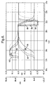
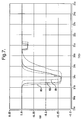
- FIG. 7 is a plot of HV1 drain current vs. time for -40° C (80), 27° C (82) and 150° C (84) operation of pre-driver circuit 25.
Landscapes
- Electronic Switches (AREA)
- Logic Circuits (AREA)
Abstract
Description
Claims (27)
- A predriver circuit for controlling a power drive circuit, comprising:a turn on drive circuit (251) having a first analog input (IN1) adapted to receive a first analog signal and an analog output (VOUT) adapted for connection to an input of a power drive circuit (18), said turn on drive circuit (251) responsive to one of an active and an inactive state of a first digital control signal (VCLK) to supply an amplified representation of said first analog signal to said analog output (VOUT), and to the other of an active and inactive state of said first digital control signal (VCLK) to disable supply of said amplified representation of said first analog signal to said analog output (VOUT); anda turn off drive circuit (252) having a second analog input (IN2) adapted to receive a second analog signal and an analog output defined by said analog output (VOUT) of said turn on drive circuit (251), said turn off drive circuit (252) responsive to the other of an active and an inactive state of said first digital control signal (VCLK) to draw an amplified representation of said second analog signal from said analog output (VOUT), and to said one of an active and an inactive state of said first digital control signal (VCLK) to disable draw of said amplified representation of said second analog signal from said analog output (VOUT).
- The predriver circuit of claim 1 wherein said turn on drive circuit (251) includes:a first analog signal amplifier (M42, M39) defining said first analog input (IN1);a second analog signal amplifier (M33, M1) coupled to said first signal amplifier (M42, M39) and defining said analog output (VOUT); anda first disabling circuit (N6, DM2, M29, M31, M32) responsive to the other of an active and an inactive state of said first digital control (VCLK) signal to disable operation of said second analog signal amplifier (M33, M1).
- The predriver circuit of claim 2 wherein said first disabling circuit includes:a first current source (M29, M31, M32); anda first logic gate (N6) responsive to said one of an active and an inactive state of said first digital control signal (VCLK) to deactivate said first current source (M29, M31, M32), and to the other of an active and an inactive state of said first digital control signal (VCLK) to activate said first current source (M29, M31, M32);
and wherein said second analog signal amplifier (M33, M1) is responsive to deactivation of said first current source (M29, M31, M32) to enable supply of said amplified representation of said first analog signal to said analog output (VOUT), and to activation of said first current source (M29, M31, M32) to disable supply of said amplified representation of said first analog signal to said analog output (VOUT). - The predriver circuit of claim 2 further including a second disabling circuit (M40, N1) responsive to the other of an active and an inactive state of said first digital control signal (VCLK) to disable operation of said first analog signal amplifier (M42, M39).
- The predriver circuit of claim 4 wherein said second disabling circuit includes:a second current source (M40); anda second logic gate (N1) responsive to said one of an active and an inactive state of said first digital control signal (VCLK) to deactivate said second current source (M40), and to the other of an active and an inactive state of said first digital control signal (VCLK) to activate said second current source (M40);
and wherein said first analog signal amplifier (M42, M39) is responsive to deactivation of said second current source (M40) to enable amplifying operation thereof, and to activation of said second current source (M40) to disable amplifying operation thereof. - The predriver circuit of claim 1 wherein said first and second analog signals each have signal magnitudes;
and wherein said signal magnitudes of said first and second analog signals are chosen to minimize electromagnetic interference produced by said predriver circuit while maximizing slew rates of said turn on and turn off drive circuits (251, 252). - A predriver circuit for controlling a power drive circuit, comprising:a first analog signal amplifier (M42, M39) defining an input adapted to receive a first analog signal;a second analog signal amplifier (M33, M1) coupled to said first analog signal amplifier (M42, M39) and defining an output (VOUT) adapted for connection to an input of a power drive circuit (18), said first and second analog signal amplifiers (M42, M39; M33, M1) responsive to a first state of a predriver control signal (VCLK) to supply an amplified representation of said first analog signal to said output (VOUT);a sense circuit (R8, Q4, M34, R13, M36, I3, I4, N1-N4, M40) responsive to detection of said amplified representation of said first analog signal to disable operation of said first analog signal amplifier (M42, M39) and a first portion (M33) of said second analog signal amplifier (M33, M1) to thereby reduce electrical power consumed thereby;a control circuit (D1-D3, R9, R10, DM3, I1, N5) responsive to disablement of said first analog signal amplifier (M42, M39) and said first portion (M33) of said second analog signal amplifier (M33, M1) to maintain a second portion (M1) of said second analog signal amplifier (M33, M1) operable to thereby maintain said output (VOUT) near a predefined signal level for a duration of said first state of said predriver control signal (VCLK); anda turn off drive circuit (252) responsive to a second state of said predriver control signal (VCLK) to draw a second analog signal from said output (VOUT).
- The predriver circuit of claim 7 wherein said first analog signal amplifier (M42, M39) includes a first transistor (M42) defining said input (IN1) thereof and a second transistor (M39) coupled to said second analog signal amplifier (M33, M1), said first and second transistors (M42, M39) decoupled from each other by a third transistor (M41) disposed therebetween.
- The predriver circuit of claim 8 wherein said sense circuit includes:an analog sensing circuit (R8, Q4, M34, R13, M36) operable to produce an analog sense signal in response to detection of said amplified representation of said first analog signal at said output (VOUT) of said second analog signal amplifier (M33, M1);a first digital logic circuit (I3, I4, N1-N4) responsive to said analog sense signal to produce a digital disable signal; anda fourth transistor (M40) operatively connected to said second transistor (M39) and responsive to said digital disable signal to disable transfer of said first analog signal from said first transistor (M42) to said second transistor (M39) to thereby disable operation of said first analog signal amplifier (M42, M39).
- The predriver circuit of claim 9 wherein said second analog signal amplifier (M33, M1) includes:a fifth transistor (M33) coupled to said second transistor (M39) of said first analog signal amplifier (M42, M39) and to a voltage source (HV1);a sixth transistor (M1) connected between said voltage source (HV1) and said output (VOUT) of said second analog signal amplifier (M33, M1);a first diode (Q2) having an anode operatively connected to said fifth transistor (M33) and a cathode; anda second diode (Q1) having an anode operatively connected to said sixth transistor (M1) and a cathode connected to said cathode of said first diode(Q2), said second analog signal amplifier thereby having said fifth transistor (M33) decoupled from said sixth transistor (M1).
- The predriver circuit of claim 10 wherein said fourth transistor (M40) is responsive to said digital disable signal to further disable current flow through said fifth transistor (M33) to thereby disable said first portion (M33) of said second analog signal amplifier (M33, M1).
- The predriver circuit of claim 10 wherein said control circuit includes:a second digital logic circuit (N5, I1) responsive to said digital disable signal to produce a digital output control signal; andan analog control circuit (DM3, R9, R10, D1-D3) responsive to said digital output control signal to maintain said sixth transistor (M1) in an on state with said output (VOUT) of said second analog signal amplifier (M33, M1) near a voltage level defined by said voltage source (HV1) for said duration of said first state of said predriver control signal (VCLK).
- The predriver circuit of claim 7 wherein said control circuit is further responsive to disablement of said first analog signal amplifier (M42, M39) and said first portion (M33) of said second analog signal amplifier (M33, M1) to maintain said second portion (M1) of said second analog signal amplifier (M33, M1) operable to thereby provide a predefined load current to said output (VOUT).
- The predriver circuit of claim 13 wherein said second portion (M1) of said second analog amplifier (M33, M1) includes an output transistor (M1) operable to source current to said output (VOUT);
and wherein said control circuit is operable to maintain said second portion (M1) of said second analog signal amplifier (M33, M1) operable to thereby provide a predefined load current to said output by maintaining a predefined on resistance of said output transistor (M1). - A predriver circuit for controlling a power drive circuit, comprising:a turn on drive circuit (251) responsive to a first state of a predriver control signal (VCLK) to supply a first analog signal to a predriver circuit output (VOUT) thereof, said predriver circuit output (VOUT) adapted for connection to an input of a power drive circuit (18);a first analog signal amplifier (M26, M27) defining an input (IN2) adapted to receive a second analog signal;a second analog signal amplifier (M24, M25) having an input coupled to said first analog signal amplifier (M26, M27) and defining a second amplifier output;a third analog signal amplifier (M13/M14, M2/M3) coupled to said second amplifier output and defining an output connected to said predriver circuit output (VOUT), said first, second and third amplifiers responsive to a second opposite state of said predriver control signal (VCLK) to draw an amplified representation of said second analog signal from said predriver circuit output (VOUT);a sense circuit (R12, DM5, M18, M23, I5, I6, N11-N13, M43) responsive to detection of said amplified representation of said second analog signal drawn from said predriver circuit output (VOUT) to disable operation of said first and second analog signal amplifiers (M26, M27; M24, M25) and a first portion (M13/M14) of said third analog signal amplifier (M13/M14, M2/M3) to thereby reduce electrical power consumed thereby; anda control circuit (N8, N9, DM4, M22, M19, M4, M5) responsive to disablement of said first and second analog signal amplifiers (M26, M27; M24, M25) and said first portion (M13/M14) of said third analog signal amplifier (M13/M14, M2/M3) to maintain a second portion (M2/M3) of said third analog signal amplifier(M13/M14, M2/M3) operable to thereby maintain said predriver circuit output (VOUT) near a predefined signal level for a duration of said second state of said predriver control signal (VCLK).
- The predriver circuit of claim 15 wherein said first analog signal amplifier (M26, M27) includes a first transistor (M26) defining said input (IN2) thereof and a second transistor (M27) coupled to said second analog signal amplifier, said first and second transistors (M26, M27) decoupled from each other by a third transistor (M44) disposed therebetween.
- The predriver circuit of claim 16 wherein said sense circuit includes:an analog sensing circuit (R12, DM5, M18, M23) operable to produce an analog sense signal in response to detection of said amplified representation of said second analog signal drawn from said output (VOUT) of said third analog signal amplifier (M13/M14, M2/M3);a first digital logic circuit (I5, I6, N10-N13) responsive to said analog sense signal to produce a digital disable signal; anda fourth transistor (M43) operatively connected to said second transistor (M27) and responsive to said digital disable signal to disable transfer of said second analog signal from said first transistor (M26) to said second transistor (M27) to thereby disable operation of said first analog signal amplifier (M26, M27).
- The predriver circuit of claim 17 wherein said second analog signal amplifier (M24, M25) includes:a fifth transistor (M25) coupled to said second transistor (M27) of said first analog signal amplifier (M26, M27) and to a voltage source (HV1); anda sixth transistor (M24) connected between said voltage source (HV1) and said output of said second analog amplifier, and operatively connected to said fifth transistor (M25) to form a current mirror.
- The predriver circuit of claim 18 wherein said third analog signal amplifier includes:a seventh transistor (M13/M14) coupled to said output of said second analog signal amplifier (M24, M25);an eighth transistor (M2/M3) connected to said output (VOUT) of said third analog signal amplifier (M13/M14, M2/M3) and coupled to a reference potential;a first diode (D7) having an anode operatively connected to said seventh transistor (M2/M3) and a cathode; anda second diode (D8) having an anode operatively connected to said eighth transistor (M2/M3) and a cathode connected to said cathode of said first diode (D7), said seventh transistor (M13/M14) thereby decoupled from said eighth transistor (M2/M3).
- The predriver circuit of claim 19 wherein said fourth transistor (M43) is responsive to said digital disable signal to further disable current flow through said seventh transistor (M13/M14) to thereby disable said first portion (M13/M14) of said third analog signal amplifier (M13/M14, M2/M3).
- The predriver circuit of claim 19 wherein said control circuit includes:a second digital logic circuit (N8, N9) responsive to said digital disable signal to produce a digital output control signal; andan analog control circuit (DM4, M22, M19, M4, M5) responsive to said digital output control signal to maintain said eighth transistor (M2/M3) in an on state with said output (VOUT) of said third analog signal amplifier (M13/M14, M2/M3) near a voltage level defined by said reference potential for said duration of said second state of said predriver control signal (VCLK).
- The predriver circuit of claim 15 wherein said control circuit is further responsive to disablement of said first and second analog signal amplifiers (M26, M27; M24, M25) and said first portion (M13/M14) of said third analog signal amplifier (M13/M14, M2/M3) to maintain said second portion (M2/M3) of said third analog signal amplifier (M13/M14, M2/M3) operable to thereby draw a predefined load current from said output (VOUT).
- The predriver circuit of claim 22 wherein said second portion of said third analog amplifier (M13/M14, M2/M3) includes at least one output transistor (M2, M3) operable to sink current from said output (VOUT);
and wherein said control circuit is operable to maintain said second portion (M2/M3) of said third analog signal amplifier (M13/M14, M2/M3) operable to thereby draw a predefined load current from said output (VOUT) by maintaining a predefined on resistance of said at least one output transistor (M2, M3). - A predriver circuit for controlling a power drive circuit, comprising:a turn on drive circuit (251) having a first analog input (IN1) adapted to receive a first analog signal and an analog output (VOUT) adapted for connection to an input of a power drive circuit (18), said turn on drive circuit (251) responsive to one of an active and an inactive state of a first digital signal (VCLK) to supply an amplified representation of said first analog signal to said analog output (VOUT) and to produce a digital turn off circuit disable signal; anda turn off drive circuit (252) having a second analog input (IN2) adapted to receive a second analog signal and an analog output defined by said analog output (VOUT) of said turn on drive circuit (251), said turn off drive circuit (252) responsive to the other of an active and inactive state of said first digital control signal (VCLK) to draw an amplified representation of said second analog signal from said analog output (VOUT) and to produce a digital turn on circuit disable signal;
wherein said turn on circuit (251) is responsive to said digital turn on circuit disable signal to disable operation thereof by disabling supply of said amplified representation of said first analog signal to said analog output (VOUT);
and wherein said turn off circuit (252) is responsive to said digital turn off circuit disable signal to disable operation thereof by disabling draw of said amplified representation of said second analog signal from said analog output (VOUT). - The predriver circuit of claim 24 wherein said turn on circuit (251) includes a first control circuit (M30, M37, R6, I2) responsive to said one of an active and an inactive state of said first digital signal (VCLK) to produce said digital turn off circuit disable signal, and to the other of an active and an inactive state of said first digital signal (VCLK) to produce a digital turn off circuit enable signal, said turn off circuit (252) responsive to said digital turn off circuit enable signal to enable operation thereof.
- The predriver circuit of claim 24 wherein said turn off circuit (252) includes a second control circuit (M20, M21, M28, R2, I8) responsive to the other of an active and an inactive state of said first digital signal (VCLK) to produce said digital turn on circuit disable signal, and to said one of an active and an inactive state of said first digital signal (VCLK) to produce a digital turn on circuit enable signal, said turn on circuit (251) responsive to said digital turn on circuit enable signal to enable operation thereof.
- The predriver circuit of claim 24 wherein said first and second analog signals each have signal magnitudes;
and wherein said magnitudes of said first and second analog signals are chosen to minimize electromagnetic interference produced by said predriver circuit while maximizing slew rates of said turn on and turn off drive circuits (251, 252).
Applications Claiming Priority (2)
| Application Number | Priority Date | Filing Date | Title |
|---|---|---|---|
| US09/290,594 US6204700B1 (en) | 1999-04-13 | 1999-04-13 | Predriver circuit for controlling a power drive circuit |
| US290594 | 1999-04-13 |
Publications (2)
| Publication Number | Publication Date |
|---|---|
| EP1045519A2 true EP1045519A2 (en) | 2000-10-18 |
| EP1045519A3 EP1045519A3 (en) | 2004-01-02 |
Family
ID=23116705
Family Applications (1)
| Application Number | Title | Priority Date | Filing Date |
|---|---|---|---|
| EP00200947A Withdrawn EP1045519A3 (en) | 1999-04-13 | 2000-03-15 | Predriver circuit for controlling a power drive circuit |
Country Status (2)
| Country | Link |
|---|---|
| US (1) | US6204700B1 (en) |
| EP (1) | EP1045519A3 (en) |
Cited By (3)
| Publication number | Priority date | Publication date | Assignee | Title |
|---|---|---|---|---|
| WO2006102927A1 (en) * | 2005-04-01 | 2006-10-05 | Freescale Semiconductor, Inc. | Charge pump and control scheme |
| EP2940444A1 (en) * | 2014-04-25 | 2015-11-04 | Jtekt Corporation | Torque detection system and electric power steering apparatus |
| CN113067566A (en) * | 2021-03-31 | 2021-07-02 | 江苏中科汉韵半导体有限公司 | High-voltage insulation isolation SiC MOSFET gate drive circuit with protection function |
Families Citing this family (12)
| Publication number | Priority date | Publication date | Assignee | Title |
|---|---|---|---|---|
| JP3285088B2 (en) * | 1999-09-08 | 2002-05-27 | 日本電気株式会社 | Waveform output device having EMI noise removal mechanism |
| IT1313850B1 (en) * | 1999-11-25 | 2002-09-24 | St Microelectronics Srl | HIGH EFFICIENCY "HIGH SIDE" CIRCUIT. |
| DE10001648C2 (en) * | 2000-01-17 | 2002-03-14 | Infineon Technologies Ag | Integrated circuit with several subcircuits |
| US6768350B1 (en) * | 2002-04-10 | 2004-07-27 | Hamilton Sundstrand Corporation | Microprocessor based solid state DC power controller |
| US7061301B2 (en) * | 2003-12-19 | 2006-06-13 | Power Integrations, Inc. | Method and apparatus switching a semiconductor switch with a multi-state drive circuit |
| JP4712519B2 (en) * | 2005-05-27 | 2011-06-29 | フリースケール セミコンダクター インコーポレイテッド | Charge pump circuit for high side drive circuit and driver drive voltage circuit |
| US7506296B1 (en) | 2006-04-18 | 2009-03-17 | Altera Corporation | Programmable logic device design tool with support for variable predriver power supply levels |
| CA2759210A1 (en) | 2009-05-11 | 2010-11-18 | Ss Sc Ip, Llc | Gate driver for enhancement-mode and depletion-mode wide bandgap semiconductor jfets |
| JP2012109916A (en) * | 2010-11-19 | 2012-06-07 | Sanken Electric Co Ltd | Load drive circuit |
| US20170033793A1 (en) * | 2015-07-31 | 2017-02-02 | Texas Instruments Incorporated | Millivolt power harvesting fet controller |
| US10128833B2 (en) | 2015-07-31 | 2018-11-13 | Texas Instruments Incorporated | Millivolt power harvesting FET controller |
| CN111181536B (en) * | 2018-11-13 | 2024-01-02 | 市光法雷奥(佛山)汽车照明系统有限公司 | switching circuit |
Family Cites Families (3)
| Publication number | Priority date | Publication date | Assignee | Title |
|---|---|---|---|---|
| JPS63187724A (en) * | 1987-01-29 | 1988-08-03 | Fanuc Ltd | Predrive circuit |
| US4829541A (en) * | 1988-01-22 | 1989-05-09 | Advanced Micro Devices, Inc. | Pseudo-ternary code transmitter |
| US5365118A (en) * | 1992-06-04 | 1994-11-15 | Linear Technology Corp. | Circuit for driving two power mosfets in a half-bridge configuration |
-
1999
- 1999-04-13 US US09/290,594 patent/US6204700B1/en not_active Expired - Lifetime
-
2000
- 2000-03-15 EP EP00200947A patent/EP1045519A3/en not_active Withdrawn
Cited By (5)
| Publication number | Priority date | Publication date | Assignee | Title |
|---|---|---|---|---|
| WO2006102927A1 (en) * | 2005-04-01 | 2006-10-05 | Freescale Semiconductor, Inc. | Charge pump and control scheme |
| US7999601B2 (en) | 2005-04-01 | 2011-08-16 | Freescale Semiconductor, Inc. | Charge pump and control scheme |
| EP2940444A1 (en) * | 2014-04-25 | 2015-11-04 | Jtekt Corporation | Torque detection system and electric power steering apparatus |
| CN113067566A (en) * | 2021-03-31 | 2021-07-02 | 江苏中科汉韵半导体有限公司 | High-voltage insulation isolation SiC MOSFET gate drive circuit with protection function |
| CN113067566B (en) * | 2021-03-31 | 2024-04-30 | 江苏中科汉韵半导体有限公司 | High-voltage insulating isolation SiC MOSFET gate driving circuit with protection function |
Also Published As
| Publication number | Publication date |
|---|---|
| EP1045519A3 (en) | 2004-01-02 |
| US6204700B1 (en) | 2001-03-20 |
Similar Documents
| Publication | Publication Date | Title |
|---|---|---|
| US6204700B1 (en) | Predriver circuit for controlling a power drive circuit | |
| US8310296B2 (en) | Driving transistor control circuit | |
| EP0685124A1 (en) | Click/pop free bias circuit | |
| JPH03185916A (en) | Adaptive gate charging circuit for power fet | |
| US20060126864A1 (en) | Circuit and method for eliminating pop noise in digital audio amplifier using dual power supply | |
| US6198350B1 (en) | Signal amplifier with fast recovery time response, efficient output driver and DC offset cancellation capability | |
| US5610486A (en) | Current mirror circuit used in a coil driver circuit of a brushless DC motor | |
| JP4557082B2 (en) | Driving transistor control circuit | |
| US6323683B1 (en) | Low distortion logic level translator | |
| JP2004088988A (en) | Load drive control system | |
| CN115528892B (en) | NMOS power tube driving circuit, chip and system | |
| US11101647B1 (en) | Overvoltage protection circuit | |
| JP3278205B2 (en) | Driver circuit and driving method | |
| CN111819648A (en) | Relay driver circuit | |
| US20040178755A1 (en) | Motor drive circuit and motor drive method that can positively perform a brake operation | |
| JP2005333736A (en) | Overcurrent preventing circuit | |
| JP2001257572A (en) | Switching element drive circuit device and electronic equipment using the same | |
| US6218873B1 (en) | Driver stage for switching a load | |
| JP2003204231A (en) | Low voltage drive circuit and method | |
| JP2000323977A (en) | Output circuit | |
| CN213478721U (en) | A DC brushless fan with zero power consumption in standby | |
| US20250055275A1 (en) | Overcurrent protection circuit, semiconductor device, electronic apparatus, and vehicle | |
| JP2009060226A (en) | Semiconductor device | |
| JP3667015B2 (en) | Power amplifier | |
| JP2004072424A (en) | MOS gate transistor gate drive circuit |
Legal Events
| Date | Code | Title | Description |
|---|---|---|---|
| PUAI | Public reference made under article 153(3) epc to a published international application that has entered the european phase |
Free format text: ORIGINAL CODE: 0009012 |
|
| AK | Designated contracting states |
Kind code of ref document: A2 Designated state(s): AT BE CH CY DE DK ES FI FR GB GR IE IT LI LU MC NL PT SE |
|
| AX | Request for extension of the european patent |
Free format text: AL;LT;LV;MK;RO;SI |
|
| PUAL | Search report despatched |
Free format text: ORIGINAL CODE: 0009013 |
|
| AK | Designated contracting states |
Kind code of ref document: A3 Designated state(s): AT BE CH CY DE DK ES FI FR GB GR IE IT LI LU MC NL PT SE |
|
| AX | Request for extension of the european patent |
Extension state: AL LT LV MK RO SI |
|
| 17P | Request for examination filed |
Effective date: 20040702 |
|
| AKX | Designation fees paid |
Designated state(s): DE FR GB |
|
| STAA | Information on the status of an ep patent application or granted ep patent |
Free format text: STATUS: THE APPLICATION IS DEEMED TO BE WITHDRAWN |
|
| 18D | Application deemed to be withdrawn |
Effective date: 20061003 |